 | –≠–ª–µ–∫—Ç—Ä–æ–Ω–Ω—ã–π –∫–æ–º–ø–æ–Ω–µ–Ω—Ç: PCM3010 | –°–∫–∞—á–∞—Ç—å:  PDF PDF  ZIP ZIP |
Document Outline
- FEATURES
- APPLICATIONS
- DESCRIPTION
- block diagram
- analog front-end (right-channel)
- Terminal Functions
- absolute maximum ratings over operating free-air temperature (unless ot\
herwise noted)
- electrical characteristics, all specifications at
- TYPICAL PERFORMANCE CURVES OF INTERNAL FILTER (ADC PORTION)
- digital filter
- analog filter
- TYPICAL PERFORMANCE CURVES OF INTERNAL FILTER (DAC PORTION)
- digital filter
- analog filter
- TYPICAL PERFORMANCE CURVES (ADC PORTION)
- TYPICAL PERFORMANCE CURVES (DAC PORTION)
- TYPICAL PERFORMANCE CURVES
- ADC output spectrum
- DAC output spectrum
- supply current
- THEORY OF OPERATION
- ADC portion
- DAC portion
- system clock
- power supply on, external reset, and power down
- PCM audio interface
- FORMAT 0: FMT[1:0] = 00
- FORMAT 1: FMT[1:0] = 01
- FORMAT 2: FMT[1:0] = 10
- FORMAT 3: FMT[1:0] = 11
- synchronization with digital audio system
- de-emphasis control
- test control
- typical circuit connection
- design and layout considerations in application
- power supply pins (V CC 1, V CC 2, V DD )
- grounding (AGND1, AGND2, DGND)
- V IN pins
- V REF 1, V REF 2 pins
- V COM pin
- system clock
- reset control
- external mute control
- MECHANICAL DATA
- DB (R-PDSO-G**) PLASTIC SMALL-OUTLINE
- IMPORTANT NOTICE
PCM3010
SLES055 ≠ NOVEMBER 2002
24-BIT STEREO AUDIO CODEC WITH 96-kHz ADC, 192-kHz DAC, AND
SINGLE-ENDED ANALOG INPUT/OUTPUT
1
www.ti.com
FEATURES
D
24-Bit Delta-Sigma ADC and DAC
D
Stereo ADC:
≠ Single-Ended Voltage Input: 3 Vp-p
≠ Antialiasing Filter Included
≠ 1/128, 1/64 Decimation Filter:
≠ Pass-Band Ripple:
±
0.05 dB
≠ Stop-Band Attenuation: ≠65 dB
≠ On-Chip High-Pass Filter: 0.84 Hz at
f
S
= 44.1 kHz
≠ High Performance:
≠ THD+N: ≠95 dB (Typical)
≠ SNR: 100 dB (Typical)
≠ Dynamic Range: 102 dB (Typical)
D
Stereo DAC:
≠ Single-Ended Voltage Output: 3 Vp-p
≠ Analog Low-Pass Filter Included
≠
◊
8 Oversampling Digital Filter:
≠ Pass-Band Ripple:
±
0.03 dB
≠ Stop-Band Attenuation: ≠50 dB
≠ High Performance:
≠ THD+N: ≠96 dB (Typical)
≠ SNR: 104 dB (Typical)
≠ Dynamic Range: 104 dB (Typical)
D
Multiple Functions:
≠ Digital De-Emphasis: 32 kHz, 44.1 kHz,
48 kHz
≠ Power Down: ADC/DAC Simultaneous
≠ 16-, 24-Bit Audio Data Formats
D
Sampling Rate: 16≠96 kHz (ADC), 16≠192 kHz
(DAC)
D
System Clock: 128 f
S
, 192 f
S
, 256 f
S
, 384 f
S
,
512 f
S
, 768 f
S
D
Dual Power Supplies: 5 V for Analog and 3.3 V
for Digital
D
Package: 24-Pin SSOP, Lead-Free Product
APPLICATIONS
D
DVD Recorders
D
CD Recorders
D
PC Audio
D
Sound Control System
DESCRIPTION
The PCM3010 is a low-cost single-chip 24-, 16-bit
stereo audio codec (ADC and DAC) with single-ended
analog voltage input and output. Both the
analog-to-digital converters (ADCs) and digital-to-
analog converters (DACs) employ delta-sigma
modulation with 64-times oversampling. The ADCs
include a digital decimation filter with a high-pass filter,
and the DACs include an 8-times-oversampling digital
interpolation filter. The DACs also include a digital
de-emphasis function. The PCM3010 accepts four
different audio data formats for the ADC and DAC. The
PCM3010 provides a power-down mode, which works
on the ADC and DAC simultaneously. The PCM3010 is
suitable for a wide variety of cost-sensitive consumer
applications where good performance is required. The
PCM3010 is fabricated using a highly advanced CMOS
process and is available in a small 24-pin SSOP
package.
This integrated circuit can be damaged by ESD. Texas Instruments recommends that all integrated circuits be handled with
appropriate precautions. Failure to observe proper handling and installation procedures can cause damage.
ESD damage can range from subtle performance degradation to complete device failure. Precision integrated circuits may be more susceptible
to damage because very small parametric changes could cause the device not to meet its published specifications.
PRODUCTION DATA information is current as of publication date.
Products conform to specifications per the terms of Texas Instruments
standard warranty. Production processing does not necessarily include
testing of all parameters.
Copyright
2002, Texas Instruments Incorporated
Please be aware that an important notice concerning availability, standard warranty, and use in critical applications of
Texas Instruments semiconductor products and disclaimers thereto appears at the end of this data sheet.
PCM3010
SLES055 ≠ NOVEMBER 2002
2
www.ti.com
1
2
3
4
5
6
7
8
9
10
11
12
24
23
22
21
20
19
18
17
16
15
14
13
V
IN
L
V
IN
R
V
REF
1
V
REF
2
V
CC
1
AGND1
FMT0
FMT1
TEST
LRCK
BCK
DIN
V
COM
V
OUT
L
V
OUT
R
V
CC
2
AGND2
DEMP0
DEMP1
PDWN
SCKI
V
DD
DGND
DOUT
DB PACKAGE
(TOP VIEW)
PACKAGE/ORDERING INFORMATION
PRODUCT
PACKAGE
PACKAGE
CODE
OPERATION
TEMPERATURE RANGE
PACKAGE
MARKING
ORDERING
NUMBER
TRANSPORT MEDIA
PCM3010DB
24 lead SSOP
24DB
25
∞
C to 85
∞
C
PCM3010
PCM3010DB
Tube
PCM3010DB
24-lead SSOP
24DB
≠25
∞
C to 85
∞
C
PCM3010
PCM3010DBR
Tape and reel
PCM3010
SLES055 ≠ NOVEMBER 2002
3
www.ti.com
block diagram
Single-End
Differential
Converter
DOUT
VINL
Reference
and Buffer
VREF1
VREF2
VINR
Fifth-Order
Delta-Sigma
Modulator
◊
1/128, 1/64
Decimation
Filter
with HPF
Power Supply
VCC2
AGND2
VCC1
AGND1
Clock and
Timing Generator,
Timing and
Power Control
Audio
Data
Interface
BCK
Single-End
Differential
Converter
Fifth-Order
Delta-Sigma
Modulator
LRCK
DIN
Analog LPF
and
Buffer Amp
TEST
VOUTL
VCOM
VOUTR
Multilevel
Delta-Sigma
Modulator
◊
8
Oversampling
Interpolation
Filter
Mode
Control
Interface
FMT0
Multilevel
Delta-Sigma
Modulator
FMT1
DEMP0
DEMP1
Analog LPF
and
Buffer Amp
VDD
DGND
SCKI
PDWN
Figure 1. PCM3010 Block Diagram
PCM3010
SLES055 ≠ NOVEMBER 2002
4
www.ti.com
analog front-end (right-channel)
VINL
1
3
4
VREF1
VREF2
10
µ
F
+
+
1
µ
F
20 k
+
≠
+
≠
Delta-Sigma
Modulator
(+)
(≠)
Reference
0.5 VCC1
0.1
µ
F
10
µ
F
+
0.1
µ
F
PCM3010
SLES055 ≠ NOVEMBER 2002
5
www.ti.com
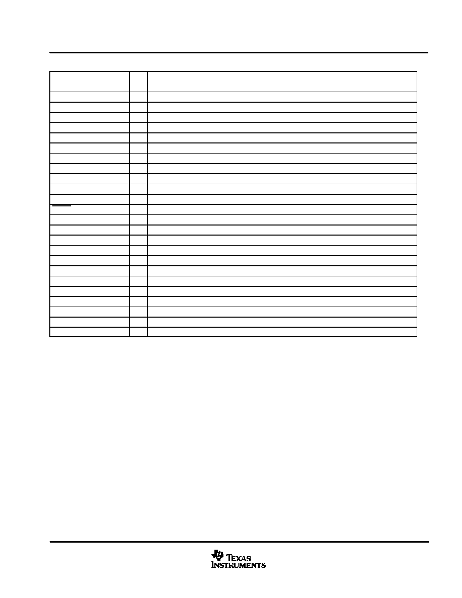
Terminal Functions
TERMINAL
I/O
DESCRIPTIONS
NAME
NO.
I/O
DESCRIPTIONS
AGND1
6
≠
ADC analog ground
AGND2
20
≠
DAC analog ground
BCK
11
I
Audio data bit clock input
DEMP1
18
I
De-emphasis select input, 1
DEMP0
19
I
De-emphasis select input, 0
DGND
14
≠
Digital ground
DIN
12
I
Audio data digital input
DOUT
13
O
Audio data digital output
FMT0
7
I
Audio data format select input, 0
FMT1
8
I
Audio data format select input, 1
LRCK
10
I
Audio data latch enable input
PDWN
17
I
ADC and DAC power-down control input, active LOW
SCKI
16
I
System clock input
TEST
9
I
Test control, must be open or connected to DGND
VCC1
5
≠
ADC analog power supply, 5 V
VCC2
21
≠
DAC analog power supply, 5 V
VCOM
24
≠
DAC common voltage decoupling (= 0.5 VCC2)
VDD
15
≠
Digital power supply, 3.3 V
VINL
1
I
ADC analog input, L-channel
VINR
2
I
ADC analog input, R-channel
VOUTL
23
O
DAC analog output, L-channel
VOUTR
22
O
DAC analog output, R-channel
VREF1
3
≠
ADC reference voltage decoupling, 1 (= 0.5 VCC1)
VREF2
4
≠
ADC reference voltage decoupling, 2
Schimtt-trigger input with 50-k
typical internal pulldown resistor, 5-V tolerant.
Schimtt-trigger input, 5-V tolerant.
PCM3010
SLES055 ≠ NOVEMBER 2002
6
www.ti.com
absolute maximum ratings over operating free-air temperature (unless otherwise noted)
Supply voltage: V
CC
1, V
CC
2
6.5 V
. . . . . . . . . . . . . . . . . . . . . . . . . . . . . . . . . . . . . . . . . . . . . . . . . . . . . . . . . . . . . . . . . . . .
V
DD
4.0 V
. . . . . . . . . . . . . . . . . . . . . . . . . . . . . . . . . . . . . . . . . . . . . . . . . . . . . . . . . . . . . . . . . . . . . . . . . . . .
Supply voltage differences: V
CC
1, V
CC
2
±
0.1 V
. . . . . . . . . . . . . . . . . . . . . . . . . . . . . . . . . . . . . . . . . . . . . . . . . . . . . . . . .
Ground voltage differences: AGND1, AGND2, DGND
±
0.1 V
. . . . . . . . . . . . . . . . . . . . . . . . . . . . . . . . . . . . . . . . . . . . . .
Digital input voltage: PDWN, TEST, FMT0, FMT1, DEMP0, DEMP1, LRCK, BCK, DIN, SCKI
≠0.3 V to +6.5 V
. . . .
Digital input voltage: DOUT
≠0.3 V to (V
DD
+ 0.3 V)
. . . . . . . . . . . . . . . . . . . . . . . . . . . . . . . . . . . . . . . . . . . . . . . . . . . . . .
Analog input voltage, V
IN
L, V
IN
R, V
REF
1, V
REF
2
≠0.3 V to (V
CC
1 + 0.3 V)
. . . . . . . . . . . . . . . . . . . . . . . . . . . . . . . . .
Analog input voltage, V
COM
, V
OUT
L, V
OUT
R
≠0.3 V to (V
CC
2 + 0.3 V)
. . . . . . . . . . . . . . . . . . . . . . . . . . . . . . . . . . . . .
Input current (any pins except supplies)
±
10 mA
. . . . . . . . . . . . . . . . . . . . . . . . . . . . . . . . . . . . . . . . . . . . . . . . . . . . . . . . .
Ambient temperature under bias
≠40
∞
C to 125
∞
C
. . . . . . . . . . . . . . . . . . . . . . . . . . . . . . . . . . . . . . . . . . . . . . . . . . . . . . . .
Storage temperature
≠55
∞
C to 150
∞
C
. . . . . . . . . . . . . . . . . . . . . . . . . . . . . . . . . . . . . . . . . . . . . . . . . . . . . . . . . . . . . . . . . . .
Junction temperature
150
∞
C
. . . . . . . . . . . . . . . . . . . . . . . . . . . . . . . . . . . . . . . . . . . . . . . . . . . . . . . . . . . . . . . . . . . . . . . . . .
Lead temperature (soldering)
260
∞
C, 5 s
. . . . . . . . . . . . . . . . . . . . . . . . . . . . . . . . . . . . . . . . . . . . . . . . . . . . . . . . . . . . . . . .
Package temperature (IR reflow, peak)
260
∞
C
. . . . . . . . . . . . . . . . . . . . . . . . . . . . . . . . . . . . . . . . . . . . . . . . . . . . . . . . . . .
Stresses beyond those listed under "absolute maximum ratings" may cause permanent damage to the device. These are stress ratings only, and
functional operation of the device at these or any other conditions beyond those indicated under "recommended operating conditions" is not
implied. Exposure to absolute-maximum-rated conditions for extended periods may affect device reliability.
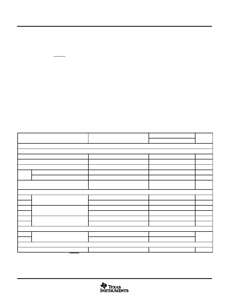
electrical characteristics, all specifications at T
A
= 25
∞
C, V
CC
1 = V
CC
2 = 5 V, V
DD
= 3.3 V,
f
S
= 44.1 kHz, SCKI = 384 f
S
, 24-bit data (unless otherwise noted)
PARAMETER
TEST CONDITIONS
PCM3010DB
UNIT
PARAMETER
TEST CONDITIONS
MIN
TYP
MAX
UNIT
DIGITAL INPUT/OUTPUT
DATA FORMAT
Audio data interface format
Left-justified, I2S, right-justified
Audio data bit length
16, 24
Bits
Audio data format
MSB-first, 2s complement
f
Sampling frequency, ADC
16
44.1
96
kHz
fS
Sampling frequency, DAC
16
44.1
192
kHz
System clock frequency
128 fS, 192 fS, 256 fS, 384 fS, 512 fS, 768
fS
4
50
MHz
INPUT LOGIC
VIH
Input logic level (see Notes 1 and 2)
2.0
5.5
VDC
VIL
Input logic level (see Notes 1 and 2)
0.8
VDC
IIH
Input logic current (see Note 2)
VIN = VDD
±
10
µ
A
IIL
Input logic current (see Note 2)
VIN = 0 V
±
10
µ
A
IIH
Input logic current (see Note 1)
VIN = VDD
65
100
µ
A
IIL
Input logic current (see Note 1)
VIN = 0 V
±
10
µ
A
OUTPUT LOGIC
VOH
Output logic level (see Note 3)
IOUT = ≠4 mA
2.4
VDC
VOL
Output logic level (see Note 3)
IOUT = 4 mA
0.4
VDC
ADC CHARACTERISTICS
Resolution
24
Bits
NOTES:
1. Pins 7, 8, 9, 17, 18, 19: PDWN , TEST, FMT0, FMT1, DEMP0, DEMP1 (Schmitt-trigger input with 50-k
typical internal pulldown
resistor, 5-V tolerant).
2. Pins 10≠12, 16: LRCK, BCK, DIN, SCKI (Schmitt-trigger input, 5-V tolerant).
3. Pin 13: DOUT.
PCM3010
SLES055 ≠ NOVEMBER 2002
7
www.ti.com
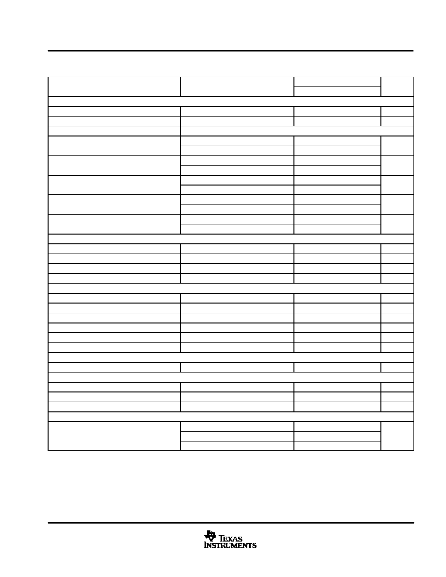
electrical characteristics, all specifications at T
A
= 25
∞
C, V
CC
1 = V
CC
2 = 5 V, V
DD
= 3.3 V,
f
S
= 44.1 kHz, SCKI = 384 f
S
, 24-bit data (unless otherwise noted) (continued)
PARAMETER
TEST CONDITIONS
PCM3010DB
UNIT
PARAMETER
TEST CONDITIONS
MIN
TYP
MAX
UNIT
ACCURACY
Gain mismatch, channel-to-channel
1 kHz, full-scale input
±
1
±
6
% of FSR
Gain error
1 kHz, full-scale input
±
2
±
6
% of FSR
DYNAMIC PERFORMANCE (see Note 4)
THD N V
0 5 dB
fS = 44.1 kHz
≠95
≠86
dB
THD+N VIN = ≠0.5 dB
fS = 96 kHz
≠92
dB
THD+N V
60 dB
fS = 44.1 kHz
≠39
dB
THD+N VIN = ≠60 dB
fS = 96 kHz
≠40
dB
Dynamic range
fS = 44.1 kHz, A-weighted
97
102
dB
Dynamic range
fS = 96 kHz, A-weighted
102
dB
S/N ratio
fS = 44.1 kHz, A-weighted
95
100
dB
S/N ratio
fS = 96 kHz, A-weighted
102
dB
Channel separation
fS = 44.1 kHz
93
98
dB
Channel separation
fS = 96 kHz
100
dB
ANALOG INPUT
Input voltage
60% of VCC1
Vp≠p
Center voltage
50% of VCC1
V
Input impedance
20
k
Anti-aliasing filter frequency response
≠3 dB
300
kHz
DIGITAL FILTER PERFORMANCE
Pass band
0.454 fS
Hz
Stop band
0.583 fS
Hz
Pass-band ripple
±
0.05
dB
Stop-band attenuation
≠65
dB
Delay time
17.4/fS
sec
HPF frequency response
≠3 dB
0.019 fS
mHz
DAC CHARACTERISTICS
Resolution
24
Bits
DC ACCURACY
Gain mismatch, channel-to-channel
±
1.0
±
4.0
% of FSR
Gain error
±
2.0
±
6.0
% of FSR
Bipolar zero error
±
1.0
% of FSR
DYNAMIC PERFORMANCE (see Note 5)
fS = 44.1 kHz
≠96
≠88
THD+N, VOUT = 0 dB
fS = 96 kHz
≠97
dB
THD+N, VOUT 0 dB
fS = 192 kHz
≠97
dB
NOTES:
4. fIN = 1 kHz, using System Two
audio measurement system, RMS mode with 20-kHz LPF, 400-Hz HPF in calculation.
5. fOUT = 1 kHz, using System Two audio measurement system, RMS mode with 20-kHz LPF, 400-Hz HPF.
System Two is a trademark of Audio Precision, Inc.
All other trademarks are the property of their respective owners.
PCM3010
SLES055 ≠ NOVEMBER 2002
8
www.ti.com
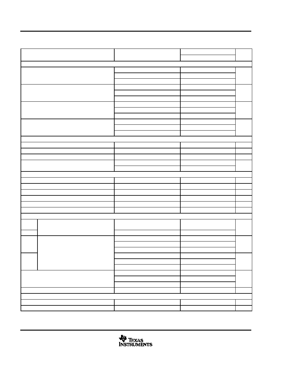
electrical characteristics, all specifications at T
A
= 25
∞
C, V
CC
1 = V
CC
2 = 5 V, V
DD
= 3.3 V,
f
S
= 44.1 kHz, SCKI = 384 f
S
, 24-bit data (unless otherwise noted) (continued)
PARAMETER
TEST CONDITIONS
PCM3010DB
UNIT
PARAMETER
TEST CONDITIONS
MIN
TYP
MAX
UNIT
DYNAMIC PERFORMANCE (see Note 5) (Continued)
fS = 44.1 kHz
≠42
THD+N VOUT = ≠60 dB
fS = 96 kHz
≠43
dB
THD+N VOUT 60 dB
fS = 192 kHz
≠43
dB
fS = 44.1 kHz, EIAJ, A-weighted
98
104
Dynamic range
fS = 96 kHz, EIAJ, A-weighted
105
dB
Dynamic range
fS = 192 kHz, EIAJ, A-weighted
105
dB
fS = 44.1 kHz, EIAJ, A-weighted
98
104
S/N ratio
fS = 96 kHz, EIAJ, A-weighted
105
dB
S/N ratio
fS = 192 kHz, EIAJ, A-weighted
105
dB
fS = 44.1 kHz
95
102
Channel separation
fS = 96 kHz
102
dB
Channel se aration
fS = 192 kHz
103
dB
ANALOG OUTPUT
Output voltage
60% of VCC2
Vp-p
Center voltage
50% of VCC2
V
Load impedance
AC coupling
5
k
LPF frequency response
f = 20 kHz
≠0.03
dB
LPF frequency response
f = 44 kHz
≠0.20
dB
DIGITAL FILTER PERFORMANCE
Pass band
±
0.03 dB
0.454 fS
Hz
Stop band
0.546 fS
Hz
Pass-band ripple
±
0.03
dB
Stop-band attenuation
0.546 fS
≠50
dB
Delay time
20/fS
sec
De-emphasis error
±
0.1
dB
POWER SUPPLY REQUIREMENTS
VCC1
VCC2
Voltage range
4.5
5.0
5.5
VDC
VDD
Voltage range
3.0
3.3
3.6
VDC
ICC
fS = 44.1 kHz
31
40
ICC
(ICC1 +
fS = 96 kHz
32
mA
(ICC1 +
ICC2)
Supply current
fS = 192 kHz
9
mA
Supply current
fS = 44.1 kHz
10
15
IDD
fS = 96 kHz
20
mA
IDD
fS = 192 kHz
14
mA
fS = 44.1 kHz
190
250
Power dissipation, operation
fS = 96 kHz
230
mW
Power dissi ation, o eration
fS = 192 kHz
90
mW
Power dissipation, power down (see Note 6)
1
mW
TEMPERATURE RANGE
Operating temperature
≠25
85
∞
C
JA
Thermal resistance
24-pin SSOP
100
∞
C/W
NOTES:
5. fOUT = 1 kHz, using System Two audio measurement system, RMS mode with 20-kHz LPF, 400-Hz HPF.
6. Halt SCKI, BCK, LRCK.
PCM3010
SLES055 ≠ NOVEMBER 2002
9
www.ti.com
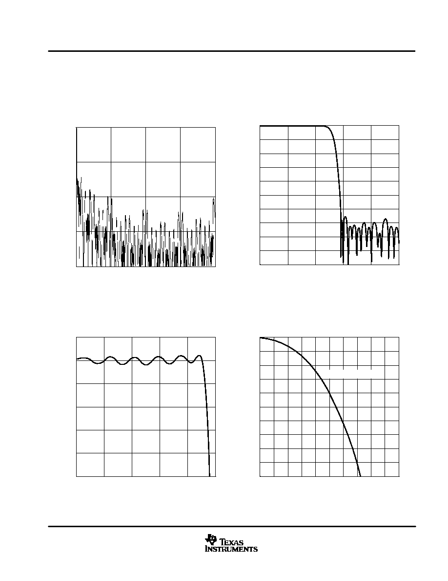
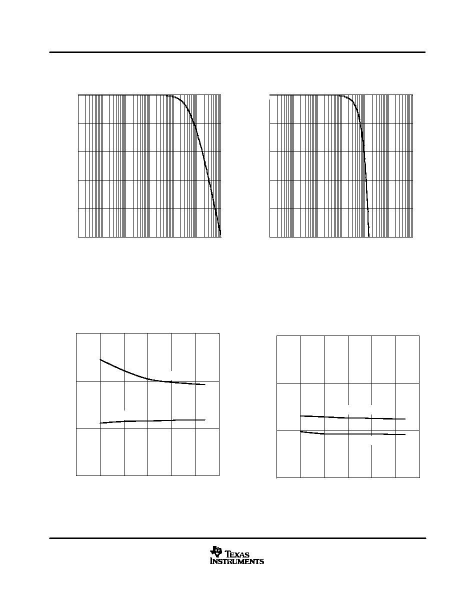
TYPICAL PERFORMANCE CURVES OF INTERNAL FILTER (ADC PORTION)
digital filter
Figure 2. Overall Characteristics
Frequency [
◊
fS]
≠200
≠150
≠100
≠50
0
0
8
16
24
32
Amplitude
≠
dB
AMPLITUDE
vs
FREQUENCY
Figure 3. Stop-Band Attenuation Characteristics
Frequency [
◊
fS]
≠100
≠90
≠80
≠70
≠60
≠50
≠40
≠30
≠20
≠10
0
0.0
0.2
0.4
0.6
0.8
1.0
Amplitude
≠
dB
AMPLITUDE
vs
FREQUENCY
≠1.0
≠0.8
≠0.6
≠0.4
≠0.2
≠0.0
0.2
0.0
0.1
0.2
0.3
0.4
0.5
Frequency [
◊
fS]
Amplitude
≠
dB
AMPLITUDE
vs
FREQUENCY
0.0
Figure 4. Pass-Band Ripple Characteristics
Figure 5. Transient Band Characteristics
Frequency [
◊
fS]
≠10
≠9
≠8
≠7
≠6
≠5
≠4
≠3
≠2
≠1
0
0.45 0.46 0.47 0.48 0.49 0.50 0.51 0.52 0.53 0.54 0.55
Amplitude
≠
dB
AMPLITUDE
vs
FREQUENCY
≠4.13 dB @ 0.5 fS
All specifications at TA = 25
∞
C, VCC1 = VCC2 = 5 V, VDD = 3.3 V, fS = 44.1 kHz, SCKI = 384 fS, 24-bit data, unless otherwise noted.
PCM3010
SLES055 ≠ NOVEMBER 2002
10
www.ti.com
digital filter (continued)
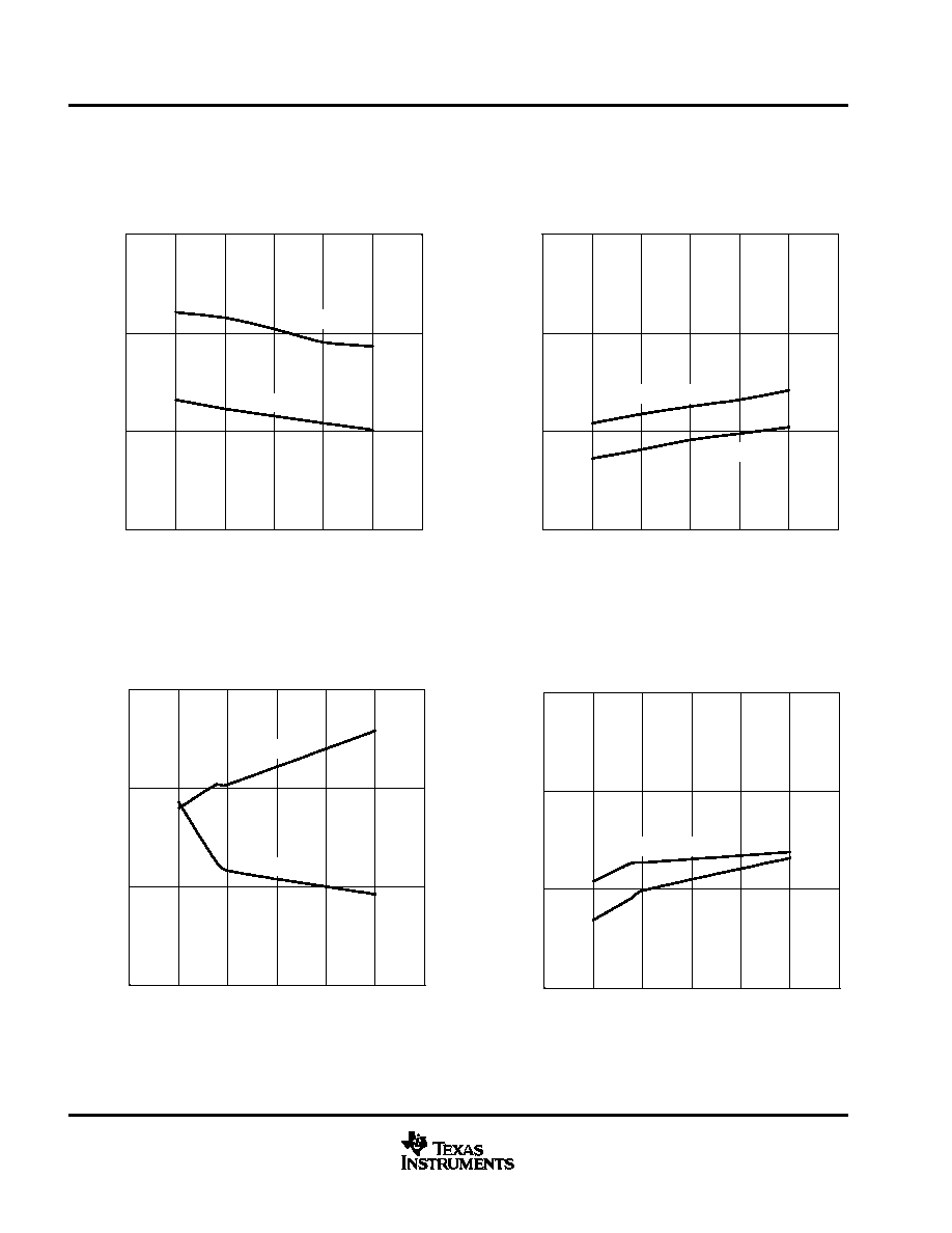
Figure 6. Low-Cut HPF Stop-Band Characteristics
Frequency [
◊
fS/1000]
≠100
≠90
≠80
≠70
≠60
≠50
≠40
≠30
≠20
≠10
0
0.0
0.1
0.2
0.3
0.4
0.5
Amplitude
≠
dB
AMPLITUDE
vs
FREQUENCY
Figure 7. Low-Cut HPF Pass-Band Characteristics
Frequency [
◊
fS/1000]
≠1.0
≠0.8
≠0.6
≠0.4
≠0.2
≠0.0
0.2
0
1
2
3
4
Amplitude
≠
dB
AMPLITUDE
vs
FREQUENCY
0.0
analog filter
Figure 8. Antialiasing Filter Stop-Band
Characteristics
≠50
≠40
≠30
≠20
≠10
0
f ≠ Frequency ≠ Hz
Amplitude
≠
dB
AMPLITUDE
vs
FREQUENCY
10
100
1k
10M
10k
100k
1M
Figure 9. Antialiasing Filter Pass-Band
Characteristics
≠1.0
≠0.8
≠0.6
≠0.4
≠0.2
≠0.0
f ≠ Frequency ≠ Hz
Amplitude
≠
dB
AMPLITUDE
vs
FREQUENCY
10
100
1k
10M
10k
100k
1M
0.0
All specifications at TA = 25
∞
C, VCC1 = VCC2 = 5 V, VDD = 3.3 V, fS = 44.1 kHz, SCKI = 384 fS, 24-bit data, unless otherwise noted.
PCM3010
SLES055 ≠ NOVEMBER 2002
11
www.ti.com
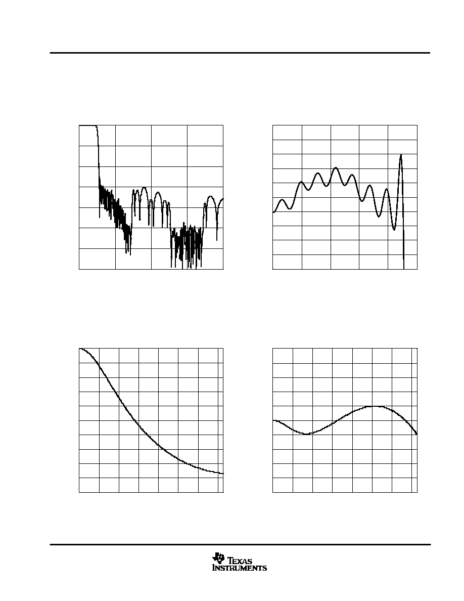
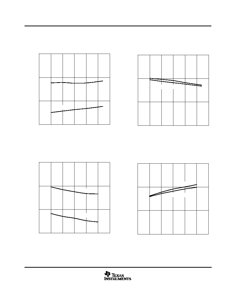
TYPICAL PERFORMANCE CURVES OF INTERNAL FILTER (DAC PORTION)
digital filter
Figure 10. Frequency Response (Sharp Rolloff)
Frequency [
◊
fS]
≠140
≠120
≠100
≠80
≠60
≠40
≠20
0
0
1
2
3
4
Amplitude
≠
dB
AMPLITUDE
vs
FREQUENCY
Figure 11. Frequency Response, Pass-Band
(Sharp Rolloff)
Frequency [
◊
fS]
≠0.05
≠0.04
≠0.03
≠0.02
≠0.01
0.00
0.01
0.02
0.03
0.04
0.05
0.0
0.1
0.2
0.3
0.4
0.5
AMPLITUDE
vs
FREQUENCY
0.00
Amplitude
≠
dB
Figure 12. De-Emphasis (f
S
= 32 kHz)
f ≠ Frequency ≠ kHz
≠10
≠9
≠8
≠7
≠6
≠5
≠4
≠3
≠2
≠1
0
0.0
2.0
4.0
6.0
8.0
10.0
12.0
14.0
LEVEL
vs
FREQUENCY
Level
≠
dB
Figure 13. De-Emphasis Error (f
S
= 32 kHz)
f ≠ Frequency ≠ kHz
≠0.5
≠0.4
≠0.3
≠0.2
≠0.1
≠0.0
0.1
0.2
0.3
0.4
0.5
0.0
2.0
4.0
6.0
8.0
10.0
12.0
14.0
ERROR
vs
FREQUENCY
0.0
Error
≠
dB
All specifications at TA = 25
∞
C, VCC1 = VCC2 = 5 V, VDD = 3.3 V, fS = 44.1 kHz, SCKI = 384 fS, 24-bit data, unless otherwise noted.
PCM3010
SLES055 ≠ NOVEMBER 2002
12
www.ti.com
digital filter (continued)
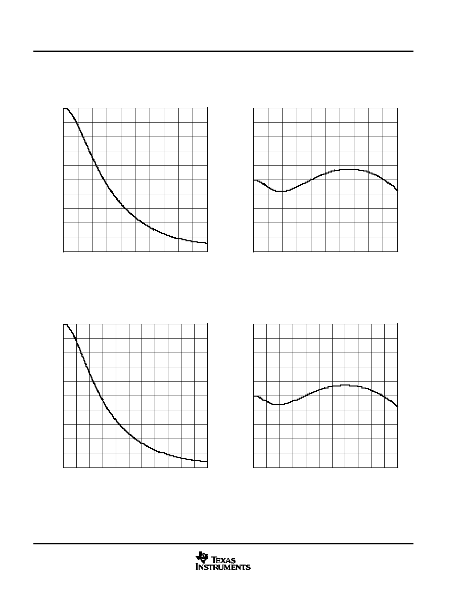
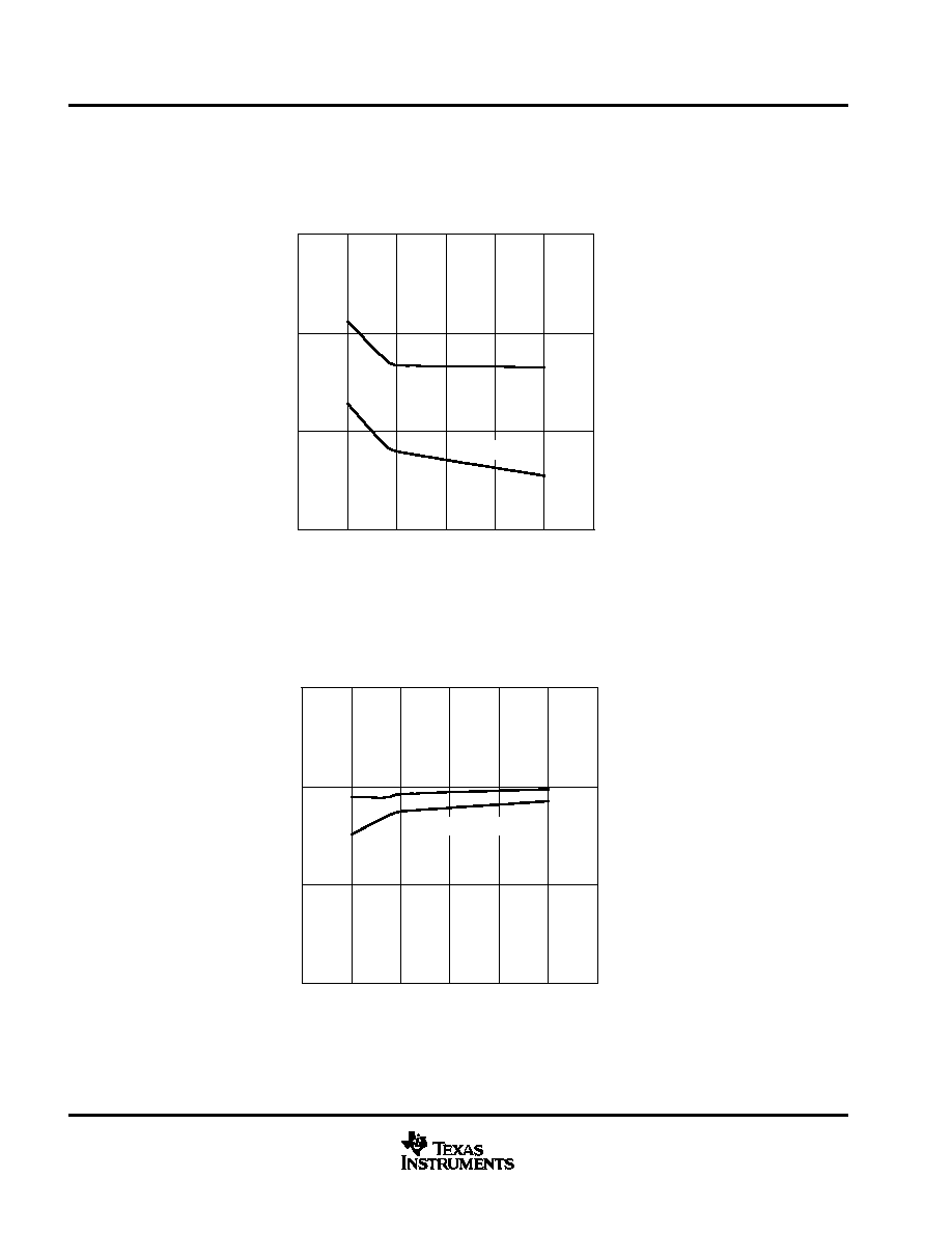
Figure 14. De-Emphasis (f
S
= 44.1 kHz)
f ≠ Frequency ≠ kHz
≠10
≠9
≠8
≠7
≠6
≠5
≠4
≠3
≠2
≠1
0
0
2
4
6
8
10
12
14
16
18
20
LEVEL
vs
FREQUENCY
Level
≠
dB
Figure 15. De-Emphasis Error (f
S
= 44.1 kHz)
f ≠ Frequency ≠ kHz
≠0.5
≠0.4
≠0.3
≠0.2
≠0.1
≠0.0
0.1
0.2
0.3
0.4
0.5
0
2
4
6
8
10
12
14
16
18
20
ERROR
vs
FREQUENCY
0.0
Error
≠
dB
Figure 16. De-Emphasis (f
S
= 48 kHz)
f ≠ Frequency ≠ kHz
≠10
≠9
≠8
≠7
≠6
≠5
≠4
≠3
≠2
≠1
0
0
2
4
6
8
10
12
14
16
18
20
22
LEVEL
vs
FREQUENCY
Level
≠
dB
Figure 17. De-Emphasis Error (f
S
= 48 kHz)
f ≠ Frequency ≠ kHz
≠0.5
≠0.4
≠0.3
≠0.2
≠0.1
≠0.0
0.1
0.2
0.3
0.4
0.5
0
2
4
6
8
10
12
14
16
18
20
22
ERROR
vs
FREQUENCY
0.0
Error
≠
dB
All specifications at TA = 25
∞
C, VCC1 = VCC2 = 5 V, VDD = 3.3 V, fS = 44.1 kHz, SCKI = 384 fS, 24-bit data, unless otherwise noted.
PCM3010
SLES055 ≠ NOVEMBER 2002
13
www.ti.com
analog filter
Figure 18. Analog Filter Stop-Band Performance
(10 Hz≠10 MHz)
≠50
≠40
≠30
≠20
≠10
0
f ≠ Frequency ≠ Hz
Amplitude
≠
dB
AMPLITUDE
vs
FREQUENCY
10
100
1k
10M
10k
100k
1M
Figure 19. Analog Filter Pass-Band Performance
(10 Hz≠10 MHz)
≠1.0
≠0.8
≠0.6
≠0.4
≠0.2
≠0.0
f ≠ Frequency ≠ Hz
Amplitude
≠
dB
10
100
1k
10M
10k
100k
1M
0.0
AMPLITUDE
vs
FREQUENCY
TYPICAL PERFORMANCE CURVES (ADC PORTION)
Figure 20
≠45
≠40
≠35
≠30
≠105
≠100
≠95
≠90
≠50
≠25
0
25
50
75
100
TA ≠ Free-Air Temperature ≠
∞
C
THD+N
≠
T
otal Harmonic Distortion + Noise at
≠
0.5 dB
≠
dB
TOTAL HARMONIC DISTORTION + NOISE
vs
FREE-AIR TEMPERATURE
THD+N
≠
T
otal Harmonic Distortion + Noise at
≠
60 dB
≠
dB
≠60 dB
≠0.5 dB
Figure 21
95
100
105
110
≠50
≠25
0
25
50
75
100
TA ≠ Free-Air Temperature ≠
∞
C
Dynamic Range and SNR
≠
dB
DYNAMIC RANGE and SNR
vs
FREE-AIR TEMPERATURE
SNR
Dynamic Range
All specifications at TA = 25
∞
C, VCC1 = VCC2 = 5 V, VDD = 3.3 V, fS = 44.1 kHz, SCKI = 384 fS, 24-bit data, unless otherwise noted.
PCM3010
SLES055 ≠ NOVEMBER 2002
14
www.ti.com
≠45
≠40
≠35
≠30
≠105
≠100
≠95
≠90
4.25
4.50
4.75
5.00
5.25
5.50
5.75
VCC ≠ Supply Voltage ≠ V
THD+N
≠
T
otal Harmonic Distortion + Noise at
≠
0.5 dB
≠
dB
TOTAL HARMONIC DISTORTION + NOISE
vs
SUPPLY VOLTAGE
THD+N
≠
T
otal Harmonic Distortion + Noise at
≠
60 dB
≠
dB
≠60 dB
≠0.5 dB
Figure 22
95
100
105
110
4.25
4.50
4.75
5.00
5.25
5.50
5.75
VCC ≠ Supply Voltage ≠ V
Dynamic Range and SNR
≠
dB
DYNAMIC RANGE and SNR
vs
SUPPLY VOLTAGE
SNR
Dynamic Range
Figure 23
≠45
≠40
≠35
≠30
≠105
≠100
≠95
≠90
16
32
48
64
80
96
112
fS ≠ Sampling Frequency ≠ kHz
THD+N
≠
T
otal Harmonic Distortion + Noise at
≠
0.5 dB
≠
dB
TOTAL HARMONIC DISTORTION + NOISE
vs
SAMPLING FREQUENCY
THD+N
≠
T
otal Harmonic Distortion + Noise at
≠
60 dB
≠
dB
≠60 dB
≠0.5 dB
Figure 24
95
100
105
110
16
32
48
64
80
96
112
fS ≠ Sampling Frequency ≠ kHz
Dynamic Range and SNR
≠
dB
DYNAMIC RANGE and SNR
vs
SAMPLING FREQUENCY
SNR
Dynamic Range
Figure 25
All specifications at TA = 25
∞
C, VCC1 = VCC2 = 5 V, VDD = 3.3 V, fS = 44.1 kHz, SCKI = 384 fS, 24-bit data, unless otherwise noted.
PCM3010
SLES055 ≠ NOVEMBER 2002
15
www.ti.com
TYPICAL PERFORMANCE CURVES (DAC PORTION)
≠45
≠40
≠35
≠30
≠105
≠100
≠95
≠90
≠50
≠25
0
25
50
75
100
TA ≠ Free-Air Temperature ≠
∞
C
THD+N
≠
T
otal Harmonic Distortion + Noise at 0 dB
≠
dB
TOTAL HARMONIC DISTORTION + NOISE
vs
FREE-AIR TEMPERATURE
THD+N
≠
T
otal Harmonic Distortion + Noise at
≠
60 dB
≠
dB
≠60 dB
0 dB
Figure 26
Figure 27
95
100
105
110
≠50
≠25
0
25
50
75
100
TA ≠ Free-Air Temperature ≠
∞
C
Dynamic Range and SNR
≠
dB
DYNAMIC RANGE and SNR
vs
FREE-AIR TEMPERATURE
SNR
Dynamic Range
≠45
≠40
≠35
≠30
≠105
≠100
≠95
≠90
4.25
4.50
4.75
5.00
5.25
5.50
5.75
VCC ≠ Supply Voltage ≠ V
THD+N
≠
T
otal Harmonic Distortion + Noise at 0 dB
≠
dB
TOTAL HARMONIC DISTORTION + NOISE
vs
SUPPLY VOLTAGE
THD+N
≠
T
otal Harmonic Distortion + Noise at
≠
60 dB
≠
dB
≠60 dB
0 dB
Figure 28
Figure 29
95
100
105
110
4.25
4.50
4.75
5.00
5.25
5.50
5.75
VCC ≠ Supply Voltage ≠ V
Dynamic Range and SNR
≠
dB
DYNAMIC RANGE and SNR
vs
SUPPLY VOLTAGE
SNR
Dynamic Range
All specifications at TA = 25
∞
C, VCC1 = VCC2 = 5 V, VDD = 3.3 V, fS = 44.1 kHz, SCKI = 384 fS, 24-bit data, unless otherwise noted.
PCM3010
SLES055 ≠ NOVEMBER 2002
16
www.ti.com
≠45
≠40
≠35
≠30
≠105
≠100
≠95
≠90
16
32
48
64
80
96
112
fS ≠ Sampling Frequency ≠ kHz
THD+N
≠
T
otal Harmonic Distortion + Noise at 0 dB
≠
dB
TOTAL HARMONIC DISTORTION + NOISE
vs
SAMPLING FREQUENCY
THD+N
≠
T
otal Harmonic Distortion + Noise at
≠
60 dB
≠
dB
≠60 dB
0 dB
Figure 30
95
100
105
110
16
32
48
64
80
96
112
fS ≠ Sampling Frequency ≠ kHz
Dynamic Range and SNR
≠
dB
DYNAMIC RANGE and SNR
vs
SAMPLING FREQUENCY
SNR
Dynamic Range
Figure 31
All specifications at TA = 25
∞
C, VCC1 = VCC2 = 5 V, VDD = 3.3 V, fS = 44.1 kHz, SCKI = 384 fS, 24-bit data, unless otherwise noted.
PCM3010
SLES055 ≠ NOVEMBER 2002
17
www.ti.com
TYPICAL PERFORMANCE CURVES
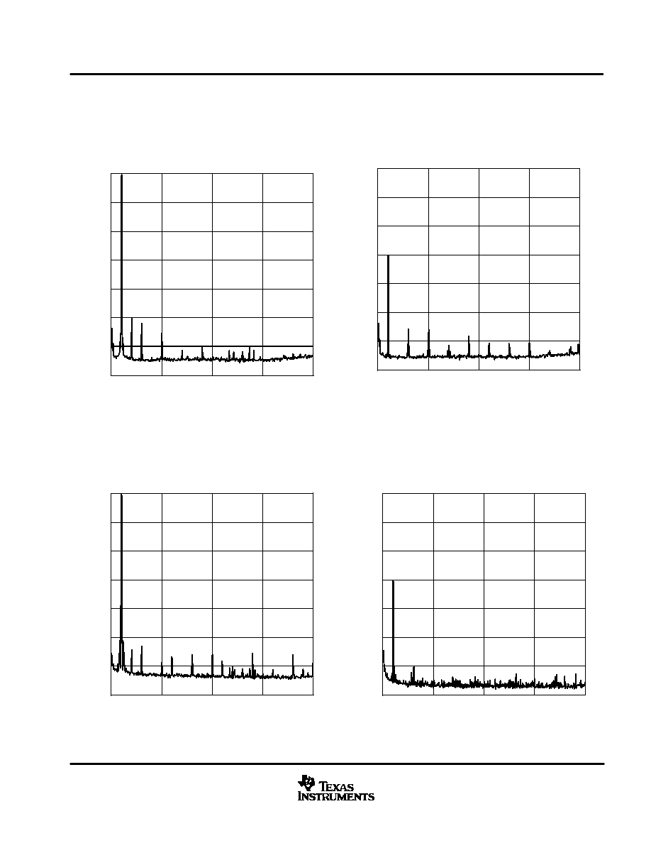
ADC output spectrum
Figure 32. Output Spectrum (≠0.5 dB, N = 8192)
f ≠ Frequency ≠ kHz
≠140
≠120
≠100
≠80
≠60
≠40
≠20
0
0
5
10
15
20
Amplitude
≠
dB
AMPLITUDE
vs
FREQUENCY
Figure 33. Output Spectrum (≠60 dB, N = 8192)
f ≠ Frequency ≠ kHz
≠140
≠120
≠100
≠80
≠60
≠40
≠20
0
0
5
10
15
20
Amplitude
≠
dB
AMPLITUDE
vs
FREQUENCY
DAC output spectrum
Figure 34. Output Spectrum (0 dB, N = 8192)
f ≠ Frequency ≠ kHz
≠140
≠120
≠100
≠80
≠60
≠40
≠20
0
0
5
10
15
20
Amplitude
≠
dB
AMPLITUDE
vs
FREQUENCY
Figure 35. Output Spectrum (≠60 dB, N = 8192)
f ≠ Frequency ≠ kHz
≠140
≠120
≠100
≠80
≠60
≠40
≠20
0
0
5
10
15
20
Amplitude
≠
dB
AMPLITUDE
vs
FREQUENCY
All specifications at TA = 25
∞
C, VCC1 = VCC2 = 5 V, VDD = 3.3 V, fS = 44.1 kHz, SCKI = 384 fS, 24-bit data, unless otherwise noted.
PCM3010
SLES055 ≠ NOVEMBER 2002
18
www.ti.com
supply current
Figure 36
0
5
10
15
20
25
30
35
≠50
≠25
0
25
50
75
100
TA ≠ Free-Air Temperature ≠
∞
C
I CC
≠
Supply Current
≠
mA
SUPPLY CURRENT
vs
FREE-AIR TEMPERATURE
ICC1 + ICC2
IDD
Figure 37. Supply Current vs Sampling Frequency,
ADC and DAC Operating
0
5
10
15
20
25
30
35
16
32
48
64
80
96
112
fS ≠ Sampling Frequency ≠ kHz
I CC
≠
Supply Current
≠
mA
SUPPLY CURRENT
vs
SAMPLING FREQUENCY
ICC1 + ICC2
IDD
Figure 38
0
5
10
15
20
25
30
35
4.25
4.50
4.75
5.00
5.25
5.50
5.75
VCC1, VCC2 ≠ Supply Voltage ≠ V
I CC
≠
Supply Current
≠
mA
SUPPLY CURRENT
vs
V
CC
1, V
CC
2 SUPPLY VOLTAGE
ICC1 + ICC2
Figure 39
0
5
10
15
20
25
30
35
2.7
3.0
3.3
3.6
3.9
VDD ≠ Supply Voltage ≠ V
I CC
≠
Supply Current
≠
mA
SUPPLY CURRENT
vs
V
DD
SUPPLY VOLTAGE
IDD
All specifications at TA = 25
∞
C, VCC1 = VCC2 = 5 V, VDD = 3.3 V, fS = 44.1 kHz, SCKI = 384 fS, 24-bit data, unless otherwise noted.
PCM3010
SLES055 ≠ NOVEMBER 2002
19
www.ti.com
THEORY OF OPERATION
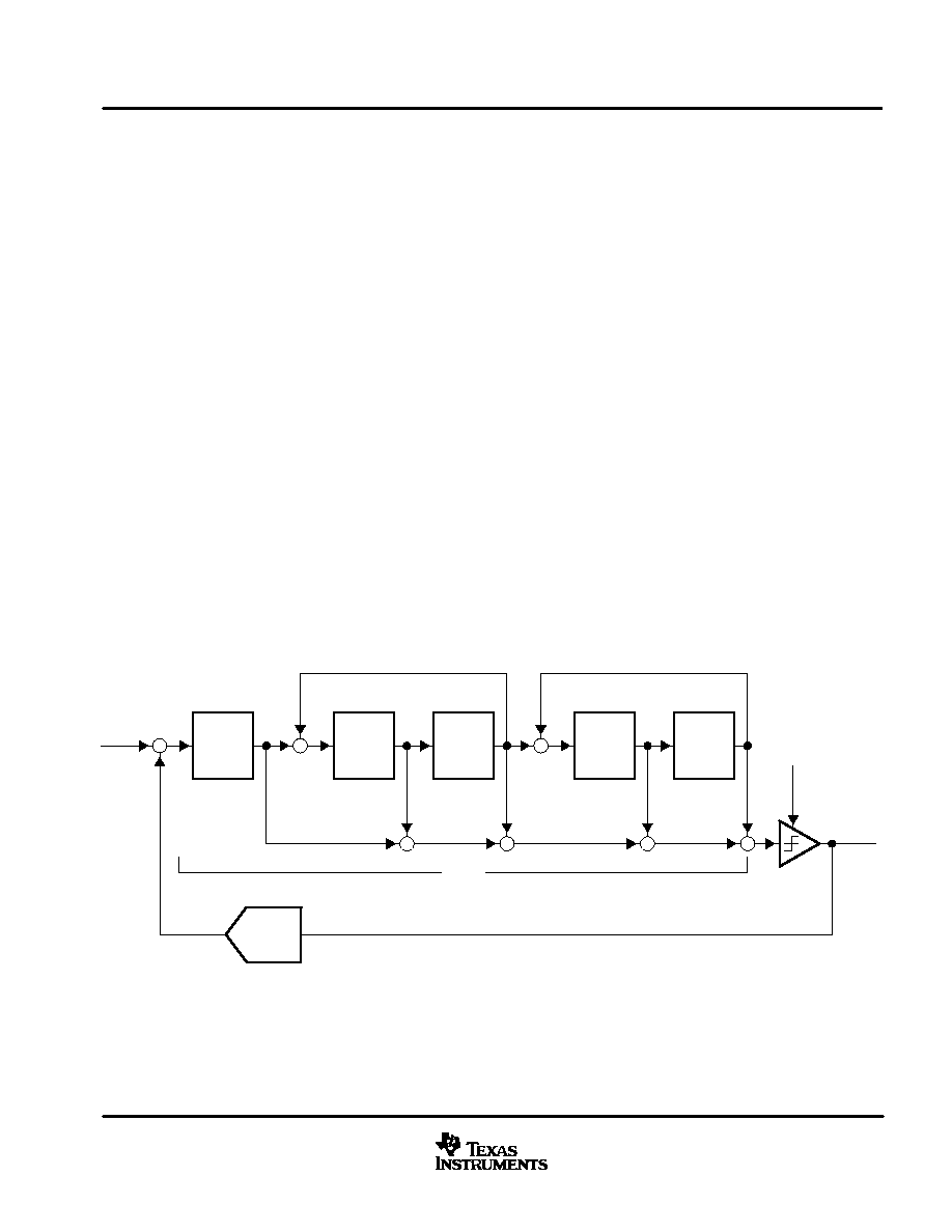
ADC portion
The ADC block consists of a reference circuit, two single-ended to differential converter channels, a fifth-order
delta-sigma modulator with full-differential architecture, a decimation filter with low-cut filter, and a serial
interface circuit which is also used as a serial interface for the DAC input signal as shown in the block diagram,
Figure 1.
The analog front-end diagram illustrates the architecture of the single-ended to differential converter and
antialiasing filter. Figure 40 illustrates the block diagram of the fifth-order delta-sigma modulator and transfer
function.
An on-chip reference circuit with two external capacitors provides all the reference voltages which are needed
in the ADC portion, and defines the full-scale voltage range of both channels.
An on-chip single-ended to differential signal converter saves the design, space, and extra parts cost of an
external signal converter.
Full-differential architecture provides a wide dynamic range and excellent power supply rejection performance.
The input signal is sampled at a
◊
64 oversampling rate, and an on-chip antialiasing filter eliminates the external
sample-hold amplifier. A fifth-order delta-sigma noise shaper, which consists of five integrators using a switched
capacitor technique followed by a comparator, shapes the quantization noise generated by the comparator and
1-bit DAC outside the audio signal band.
The high order delta-sigma modulation randomizes the modulator outputs and reduces the idle tone level.
The 64-f
S
, 1-bit stream from the delta-sigma modulator is converted to a 1-f
S
, 24-bit or 16-bit digital signal by
removing the high-frequency noise components with a decimation filter.
The dc component of the signal is removed by the HPF, and the HPF output is converted to a time-multiplexed
serial signal through the serial interface, which provides flexible serial formats.
1st
SW-CAP
Integrator
Analog
In
X(z)
+
≠
+
≠
2nd
SW-CAP
Integrator
3rd
SW-CAP
Integrator
+
≠
4th
SW-CAP
Integrator
+
+
+
+
+
+
+
+
5th
SW-CAP
Integrator
Digital
Out
Y(z)
Comparator
Qn(z)
H(z)
1-Bit
DAC
STF(z) = H(z) / [1 + H(z)]
NTF(z) = 1 / [1 + H(z)]
Y(z) = STF(z) * X(z) + NTF(z) * Qn(z)
Signal Transfer Function
Noise Transfer Function
Figure 40. Block Diagram of Fifth-Order Delta-Sigma Modulator
PCM3010
SLES055 ≠ NOVEMBER 2002
20
www.ti.com
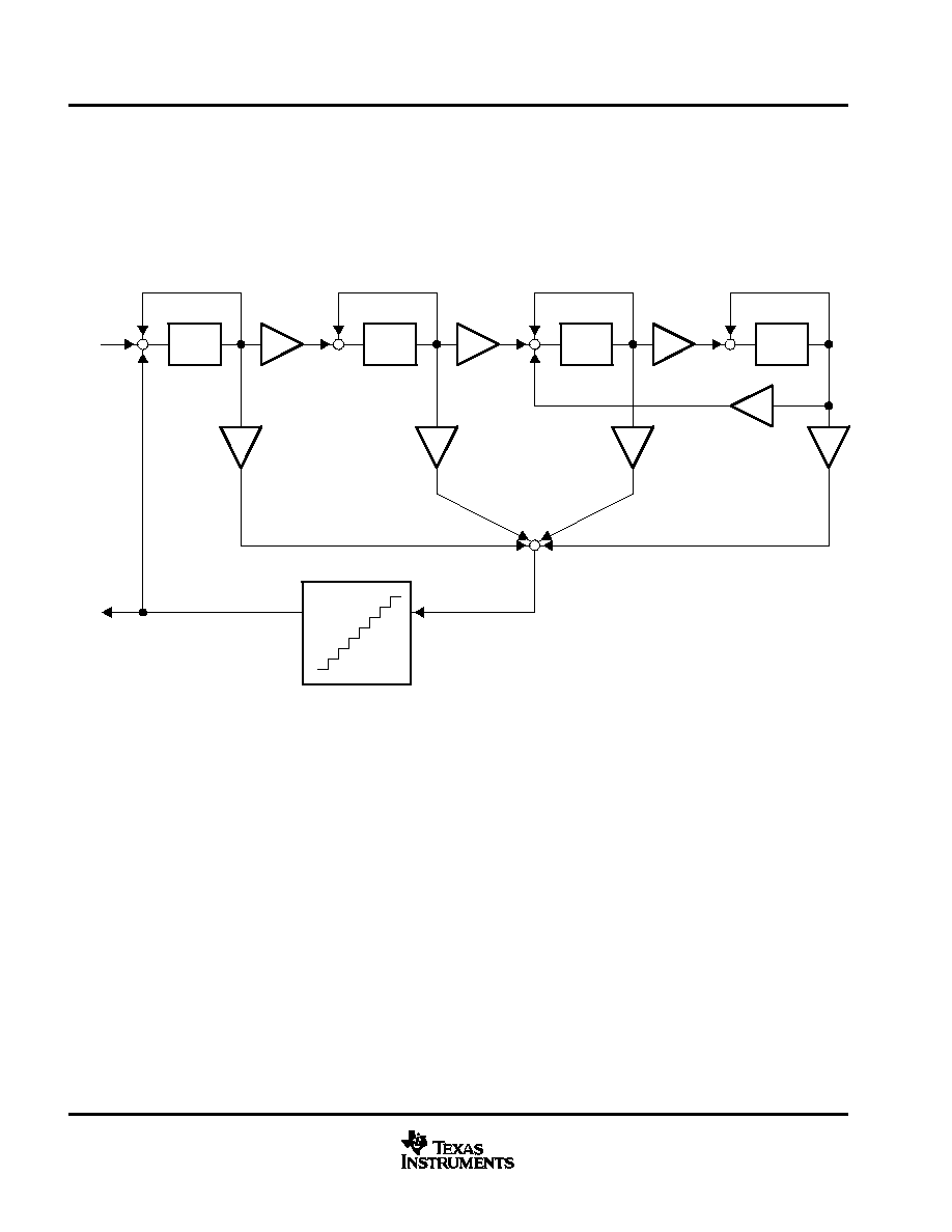
DAC portion
The DAC portion is based on the delta-sigma modulator, which consists of an 8-level amplitude quantizer and
a 4th-order noise shaper. This section converts the oversampled input data to the 8-level delta-sigma format.
A block diagram of the 8-level delta-sigma modulator is shown in Figure 41. This 8-level delta-sigma modulator
has the advantage of improved stability and clock jitter over the typical one-bit (2-level) delta-sigma modulator.
The combined oversampling rate of the delta-sigma modulator and the internal 8
◊
interpolation filter is 64 f
S
for
all system clocks. The theoretical quantization noise performance of the 8-level delta-sigma modulator is shown
in Figure 42.
+
+
≠
Z≠1
+
+
+
+
+
+
8-Level Quantizer
≠
Z≠1
IN
8 fS
OUT
64 fS
+
+
Z≠1
+
+
Z≠1
Figure 41. 8-Level Delta-Sigma Modulator Block Diagram

PCM3010
SLES055 ≠ NOVEMBER 2002
21
www.ti.com
Frequency [
fS]
≠180
≠160
≠140
≠120
≠100
≠80
≠60
≠40
≠20
0
0
1
2
3
4
5
6
7
8
AMPLITUDE
vs
FREQUENCY
Amplitude
≠
dB
Jitter ≠ ps
90
95
100
105
110
115
120
125
0
100
200
300
400
500
600
DYNAMIC RANGE
vs
JITTER
Dynamic
Range
≠
dB
Figure 42. Quantization Noise Spectrum
(
64 Oversampling)
Figure 43. Jitter Dependence
(
64 Oversampling)
system clock
The system clock for the PCM3010 must be 128 f
S
, 192 f
S
, 256 f
S
, 384 f
S
, 512 f
S
or 768 f
S
, where f
S
is the audio
sampling rate, 16 kHz to 192 kHz. The PCM3010 detects 128 f
S
, 192 f
S
, 256 f
S
, 384 f
S
, 512 f
S
or 768 f
S
automatically with the built-in circuit. Operation at the 192-kHz sampling rate is available on the DAC only, and
when a system clock of 128 f
S
or 192 f
S
is detected, the ADC is disabled (DOUT = LOW). Table 1 lists the typical
system clock frequency, and Figure 44 illustrates the system clock timing.
Table 1. Typical System Clock
SAMPLING RATE
SYSTEM CLOCK FREQUENCY ≠ MHz
FREQUENCY (fS) ≠ LRCK
128 fS
192 fS
256 fS
384 fS
512 fS
768 fS
32 kHz
≠
≠
8.192
12.288
16.384
24.576
44.1 kHz
≠
≠
11.2896
16.9344
22.5792
33.8688
48 kHz
≠
≠
12.288
18.432
24.576
36.864
96 kHz
≠
≠
24.576
36.864
49.152
≠
192 kHz
24.576
36.864
≠
≠
≠
≠
DAC only.
PCM3010
SLES055 ≠ NOVEMBER 2002
22
www.ti.com
system clock (continued)
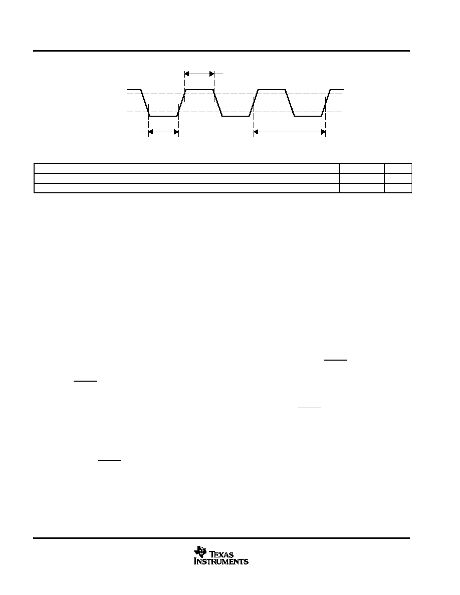
tSCKH
System Clock
0.8 V
2.0 V
tSCKL
1/128 fS or 1/192 fS
1/256 fS or 1/384 fS
1/512 fS or 1/768 fS
PARAMETER
MIN
MAX
UNIT
tSCKH
System clock pulse duration HIGH
8
ns
tSCKL
System clock pulse duration LOW
8
ns
Figure 44. System Clock Timing
power supply on, external reset, and power down
The PCM3010 has both an internal power-on reset circuit and an external reset circuit. The sequences for both
resets are explained as follows.
Figure 45 is the timing diagram for the internal power-on reset. Two power-on reset circuits are implemented
for V
CC
1 and V
DD
, respectively. Initialization (reset) occurs automatically when V
CC
1 and V
DD
exceed 4.0 V and
2.2 V, typically.
Internal reset is released 1024 SCKI clock cycles following the release from power-on reset, and the PCM3010
begins normal operation. V
OUT
L and V
OUT
R from the DAC are forced to the V
COM
(= 0.5 V
CC
2) level as V
CC
2
rises. When synchronization between SCKI, BCK and LRCK is obtained while V
OUT
L and V
OUT
R go into the
fade sequence and provide outputs corresponding to DIN after t
DACDLY1
= 2100/f
S
following release from
power-on reset. On the other hand, DOUT from the ADC provides an output corresponding to V
IN
L and V
IN
R
after t
ADCDLY1
= 4500/f
S
following release from power-on reset. If the synchronization is not held, the internal
reset is not released and device operation remains in the power-down mode. After resynchronization, the DAC
performs the fade-in sequence and the ADC resumes normal operation following internal initialization.
Figure 46 is the external-reset timing diagram. External forced reset, driving the PDWN pin LOW, puts the
PCM3010 in the power-down mode, which is its lowest power-dissipation state.
When PDWN transitions from HIGH to LOW while synchronization is maintained between SCKI, BCK, and
LRCK, then V
OUT
L and V
OUT
R are faded out and forced to the V
COM
(= 0.5 V
CC
2) level after t
DACDLY1
= 2100/f
S
.
At the same time as the internal reset becomes LOW, DOUT becomes ZERO, the PCM3010 enters into
power-down mode. To enter into normal operation mode again, change PDWN to HIGH again. The reset
sequence shown in Figure 45 occurs.
Notes:
1.
A large popping noise may be generated on V
OUT
L and V
OUT
R when the power supply is turned off during
normal operation.
2.
To switch PDWN during fade in or fade out causes an immediate change between fade in and fade out.
3.
To switch the control pins on the fly during normal operation can degrade analog performance. It is
recommended that changing control pins, changing clocks, stopping clocks, turning power supplies off, etc.,
be done in the power-down mode.
PCM3010
SLES055 ≠ NOVEMBER 2002
23
www.ti.com
power supply on, external reset and power down (continued)
Zero
VCC1, VDD
(VCC1 = 5 V,
VDD = 3.3 V, Typ)
0 V
(VCC1 = 4 V, VDD = 2.2 V, Typ)
LRCK, BCK, SCKI
PDWN
Internal Reset
VOUTL, VOUTR
DOUT
Synchronous Clocks
1024 SCKI
Power Down
Normal Operation
tDACDLY1 2100/fS
VCOM (0.5 VCC2)
tADCDLY1 4500/fS
Figure 45. DAC Output and ADC Output for Power-On Reset
DOUT
VCC1, VDD
0 V
Synchronous Clocks
LRCK, BCK, SCKI
Synchronous Clocks
PDWN
Internal Reset
Power Down
Normal Operation
1024 SCKI
Normal Operation
VOUTL, VOUTR
Zero
VCOM (0.5 VCC2)
tADCDLY1 4500/fS
tDACDLY1
2100/fS
tDACDLY1
2100/fS
(VCC1 = 5 V,
VDD = 3.3 V, Typ)
Figure 46. DAC Output and ADC Output for External Reset (PDWN Pin)
PCM3010
SLES055 ≠ NOVEMBER 2002
24
www.ti.com
PCM audio interface
Digital audio data is interfaced to the PCM3010 on LRCK (pin 10), BCK (pin 11), DIN (pin 12), and DOUT
(pin 13). The PCM3010 can accept the following 16-bit and 24-bit formats. These formats are selected through
FMT0 (pin 7) and FMT1 (pin 8), as shown in Table 2.
Table 2. Audio Data Format Select
FMT1
FMT0
DAC DATA FORMAT
ADC DATA FORMAT
LOW
LOW
24-bit, MSB-first, right-justified
24-bit, MSB-first, left-justified
LOW
HIGH
16-bit, MSB-first, right-justified
24-bit, MSB-first, left-justified
HIGH
LOW
24-bit, MSB-first, left-justified
24-bit, MSB-first, left-justified
HIGH
HIGH
24-bit, MSB-first, I2S
24-bit, MSB-first, I2S
The PCM3010 accepts two combinations of BCK and LRCK, 64 or 48 clocks of BCK in one clock of LRCK. The
following figures illustrate audio data input/output format and timing.
FORMAT 0: FMT[1:0] = 00
DAC: 24-Bit, MSB-First, Right-Justified
LRCK
Right Channel
Left Channel
BCK
DIN
24
22 23 24
3
2
1
MSB
LSB
22 23 24
3
2
1
MSB
LSB
ADC: 24-Bit, MSB-First, Left-Justified
BCK
LRCK
Right Channel
Left Channel
DOUT
1
22 23 24
3
2
1
MSB
LSB
22 23 24
3
2
1
MSB
LSB
FORMAT 1: FMT[1:0] = 01
LRCK
Right Channel
Left Channel
BCK
DIN
16
14 15 16
3
2
1
MSB
LSB
14 15 16
3
2
1
MSB
LSB
DAC: 16-Bit, MSB-First, Right-Justified
ADC: 24-Bit, MSB-First, Left-Justified
BCK
LRCK
Right Channel
Left Channel
DOUT
1
22 23 24
3
2
1
MSB
LSB
22 23 24
3
2
1
MSB
LSB
Figure 47. Audio Data Input/Output Format
PCM3010
SLES055 ≠ NOVEMBER 2002
25
www.ti.com
PCM audio interface (continued)
FORMAT 2: FMT[1:0] = 10
LRCK
BCK
DIN
DAC: 24-Bit, MSB-First, Left-Justified
ADC: 24-Bit, MSB-First, Left-Justified
BCK
LRCK
Right Channel
Left Channel
DOUT
1
22 23 24
3
2
1
MSB
LSB
22 23 24
3
2
1
MSB
LSB
Right Channel
Left Channel
1
22 23 24
3
2
1
MSB
LSB
22 23 24
3
2
1
MSB
LSB
FORMAT 3: FMT[1:0] = 11
DAC: 24-Bit, MSB-First, I2S
LRCK
Right Channel
Left Channel
BCK
DIN
22 23 24
3
2
1
MSB
LSB
22 23 24
3
2
1
MSB
LSB
ADC: 24-Bit, MSB-First, I2S
LRCK
Right Channel
Left Channel
BCK
DOUT
22 23 24
3
2
1
MSB
LSB
22 23 24
3
2
1
MSB
LSB
Figure 48. Audio Data Input/Output Format (Continued)
PCM3010
SLES055 ≠ NOVEMBER 2002
26
www.ti.com
PCM audio interface (continued)
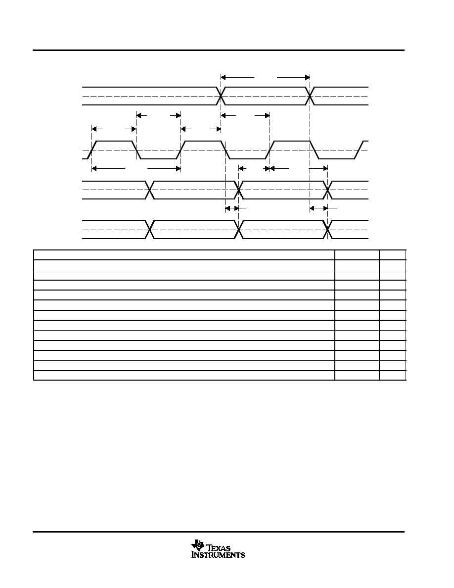
BCK
LRCK
DIN
tBCH
tBCL
tLRP
tLB
tBCY
1.4 V
1.4 V
1.4 V
tBL
DOUT
tCKDO
tLRDO
0.5 VDD
tDIS
tDIH
PARAMETER
MIN
MAX
UNIT
tBCY
BCK pulse cycle time
80
ns
tBCH
BCK pulse duration, HIGH
35
ns
tBCL
BCK pulse duration, LOW
35
ns
tBL
BCK rising edge to LRCK edge
10
ns
tLB
LRCK edge to BCK rising edge
10
ns
tLRP
LRCK pulse duration
2.1
µ
s
tDIS
DIN setup time
10
ns
tDIH
DIN hold time
10
ns
tCKDO
DOUT delay time from BCK falling edge
20
ns
tLRDO
DOUT delay time from LRCK edge
20
ns
tR
Rising time of all signals
10
ns
tF
Falling time of all signals
10
ns
Figure 49. Audio Data Input/Output Timing
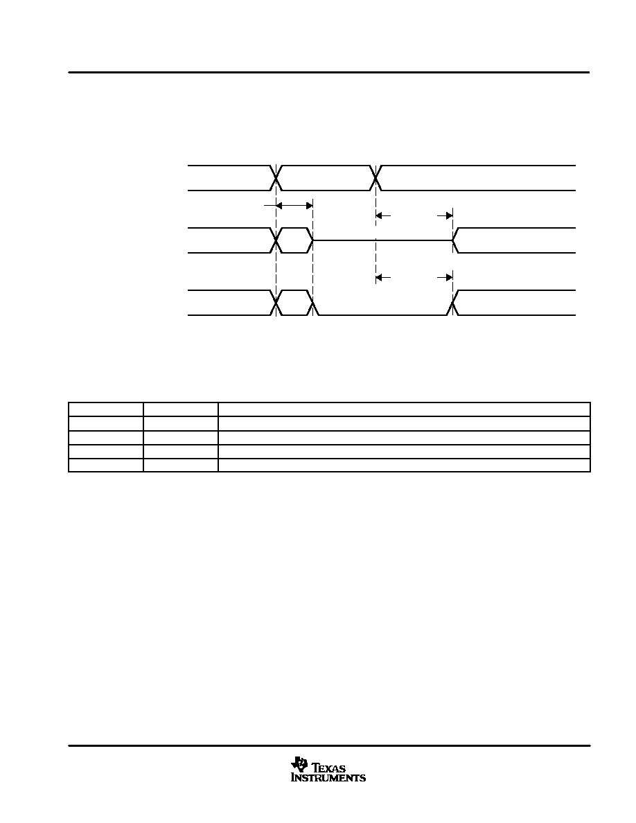
synchronization with digital audio system
The PCM3010 operates with LRCK and BCK synchronized to the system clock. The PCM3010 does not need
a specific phase relationship between LRCK, BCK and the system clock, but does require the synchronization
of LRCK, BCK, and the system clock.
If the relationship between system clock and LRCK changes more than
±
6 BCKs during one sample period due
to LRCK jitter, etc., internal operation of DAC halts within 6/f
S
, and the analog output is forced to 0.5 V
CC
2 until
resynchronization between the system clock, LRCK, and BCK is completed and then t
DACDLY2
elapses.
Internal operation of the ADC also halts within 6/f
S
, and the digital output is forced to a ZERO code until
resynchronization between the system clock, LRCK, and BCK is completed, and then t
ADCDLY2
elapses.
In the case of changes less than
±
5 BCKs, resynchronization does not occur and the previously described
discontinuity in analog/digital output control does not occur.
PCM3010
SLES055 ≠ NOVEMBER 2002
27
www.ti.com
synchronization with digital audio system (continued)
Figure 50 illustrates the DAC analog output and ADC digital output for loss of synchronization.
During undefined data, some noise may be generated in the audio signal. Also, the transition from normal to
undefined data and from undefined or zero data to normal creates a data discontinuity on the analog and digital
outputs, which may generate some noise in the audio signal.
Within 6/fS
tDACDLY2
32/fS
NORMAL DATA
UNDEFINED
DATA
NORMAL DATA
SYNCHRONOUS
ASYNCHRONOUS
SYNCHRONOUS
DAC VOUT
State of Synchronization
NORMAL DATA
ZERO DATA
UNDEFINED
DATA
NORMAL DATA
ADC DOUT
VCOM (0.5 VCC2)
tADCDLY2
32/fS
Figure 50. DAC Output and ADC Output for Lost of Synchronization
de-emphasis control
DEMP1, DEMP0: De-emphasis control pins select the de-emphasis mode of the DACs as shown below.
DEMP1
DEMP0
DESCRIPTION
LOW
LOW
De-emphasis 44.1 kHz ON
LOW
HIGH
De-emphasis OFF
HIGH
LOW
De-emphasis 48 kHz ON
HIGH
HIGH
De-emphasis 32 kHz ON
test control
TEST: The TEST pin is used for device testing; it must be connected to DGND for normal operation.
PCM3010
SLES055 ≠ NOVEMBER 2002
28
www.ti.com
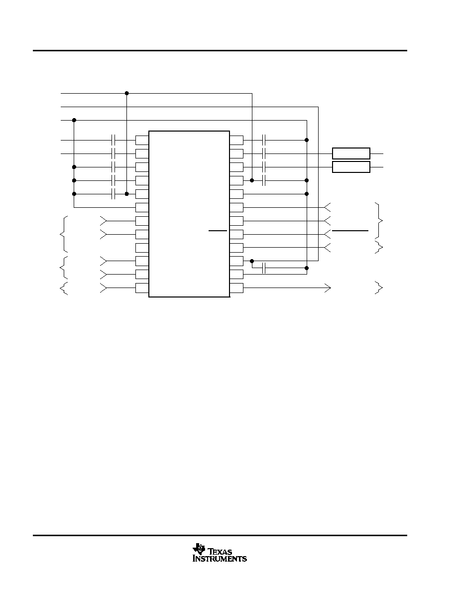
typical circuit connection
The following figure illustrates typical circuit connection.
VCC1
20
19
18
17
16
15
14
13
5
6
7
8
9
10
11
12
AGND1
FMT0
FMT1
TEST
LRCK
BCK
DIN
AGND2
DOUT
DEMP0
DEMP1
PDWN
SCKI
DGND
VDD
L-Ch IN
Format 0
Clock
De-emphasis 0
(See Note C)
Control
VINL
24
23
22
21
1
2
3
4
VINR
VREF1
VREF2
VCOM
VOUTL
VOUTR
VCC2
+
+
(See Note B)
+
(See Note B)
+
(See Note A)
+
NOTES: A. 0.1
µ
F ceramic and 10
µ
F electrolytic capacitors typical, depending on power supply quality and pattern layout.
B. 0.1
µ
F ceramic and 10
µ
F electrolytic capacitors are recommended.
C. 1
µ
F electrolytic capacitor typical, gives 8-Hz cutoff frequency of input HPF in normal operation and gives settling time with
20 ms (1
µ
F
◊
20 k
) time constant in power ON and power down OFF period.
D. 10
µ
F electrolytic capacitor typical, gives 2-Hz cutoff frequency for 10-k
post-LPF input resistance in normal operation and
gives settling time with 100 ms (10
µ
F
◊
10 k
) time constant in power ON and power down OFF period.
R-Ch IN
0 V
3.3 V
5 V
Format 1
L/R Clock
Data IN
Bit Clock
Control
Data
+
(See Note B)
(See Note D)
(See Note D)
(See Note A)
+
+
+
(See Note C)
Post LPF
Post LPF
De-emphasis 1
Power Down
System Clock
Clock
Data OUT
Data
+
(See Note A)
design and layout considerations in application
power supply pins (V
CC
1, V
CC
2, V
DD
)
The digital and analog power supply lines to the PCM3010 should be bypassed to the corresponding ground
pins, with 0.1-
µ
F ceramic and 10-
µ
F electrolytic capacitors as close to the pins as possible to maximize the
dynamic performance of the ADC and the DAC.
Although the PCM3010 has three power lines to maximize the potential of dynamic performance, using one
common 5-V power supply for V
CC
1 and V
CC
2 and a 3.3-V power supply, which is generated from the 5-V V
CC
1
and V
CC
2 power supply, for V
DD
. This power supply arrangement is recommended to avoid unexpected power
supply trouble, like latch-up or power supply sequencing problems.
grounding (AGND1, AGND2, DGND)
To maximize the dynamic performance of the PCM3010, the analog and digital grounds are not connected
internally. These points should have very low impedance to avoid digital noise feeding back into the analog
ground. They should be connected directly to each other under the connected parts to reduce the potential for
noise problems.

PCM3010
SLES055 ≠ NOVEMBER 2002
29
www.ti.com
V
IN
pins
A 1-
µ
F electrolytic capacitor is recommended as an ac-coupling capacitor, which gives an 8-Hz cutoff frequency.
If a higher full-scale input voltage is required, it can be adjusted by adding only one series resistor to each V
IN
pin.
V
REF
1, V
REF
2 pins
A 0.1-
µ
F ceramic capacitor and a 10-
µ
F electrolytic capacitor are recommended between V
REF
1, V
REF
2, and
AGND1 to ensure low source impedance of the ADC references. These capacitors should be located as close
as possible to the V
REF
1 and V
REF
2 pins and the AGND1 pin to reduce dynamic errors on the ADC references.
V
COM
pin
A 0.1-
µ
F ceramic capacitor and a 10-
µ
F electrolytic capacitor are recommended between V
COM
and AGND2
to ensure low source impedance of the DAC common voltage. These capacitors should be located as close as
possible to the V
COM
pin to reduce dynamic errors on the DAC common voltage.
system clock
The quality of SCKI may influence dynamic performance, as the PCM3010 (both DAC and ADC) operates
based on SCKI. Therefore, it may be necessary to consider the jitter, duty cycle, rise and fall time, etc., of the
system clock.
reset control
If large capacitors (more than 22
µ
F) are used on V
REF
1, V
REF
2, and V
COM
, external reset control by
PDWN = LOW is required after the V
REF
1, V
REF
2, and V
COM
transient response settles.
external mute control
To eliminate the clicking noise which is generated by DAC output dc level change during power-down ON/OFF
control, external mute control is generally required. The recommended control sequence is: external mute ON,
codec power down ON, SCKI stop and restart if necessary, codec power down OFF, and external mute OFF.
PCM3010
SLES055 ≠ NOVEMBER 2002
30
www.ti.com
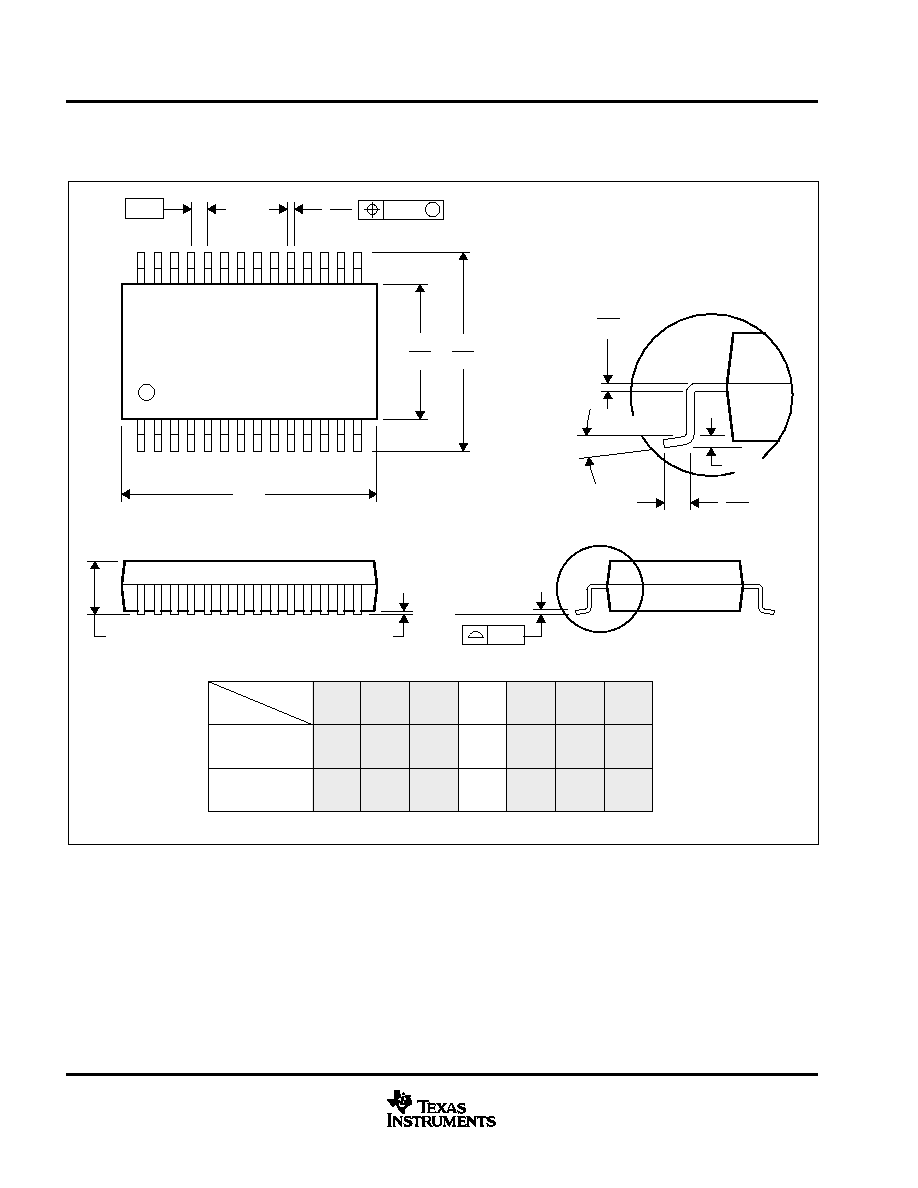
MECHANICAL DATA
DB (R-PDSO-G**)
PLASTIC SMALL-OUTLINE
4040065 /E 12/01
28 PINS SHOWN
Gage Plane
8,20
7,40
0,55
0,95
0,25
38
12,90
12,30
28
10,50
24
8,50
Seating Plane
9,90
7,90
30
10,50
9,90
0,38
5,60
5,00
15
0,22
14
A
28
1
20
16
6,50
6,50
14
0,05 MIN
5,90
5,90
DIM
A MAX
A MIN
PINS **
2,00 MAX
6,90
7,50
0,65
M
0,15
0
∞
≠ 8
∞
0,10
0,09
0,25
NOTES: A. All linear dimensions are in millimeters.
B. This drawing is subject to change without notice.
C. Body dimensions do not include mold flash or protrusion not to exceed 0,15.
D. Falls within JEDEC MO-150

IMPORTANT NOTICE
Texas Instruments Incorporated and its subsidiaries (TI) reserve the right to make corrections, modifications,
enhancements, improvements, and other changes to its products and services at any time and to discontinue
any product or service without notice. Customers should obtain the latest relevant information before placing
orders and should verify that such information is current and complete. All products are sold subject to TI's terms
and conditions of sale supplied at the time of order acknowledgment.
TI warrants performance of its hardware products to the specifications applicable at the time of sale in
accordance with TI's standard warranty. Testing and other quality control techniques are used to the extent TI
deems necessary to support this warranty. Except where mandated by government requirements, testing of all
parameters of each product is not necessarily performed.
TI assumes no liability for applications assistance or customer product design. Customers are responsible for
their products and applications using TI components. To minimize the risks associated with customer products
and applications, customers should provide adequate design and operating safeguards.
TI does not warrant or represent that any license, either express or implied, is granted under any TI patent right,
copyright, mask work right, or other TI intellectual property right relating to any combination, machine, or process
in which TI products or services are used. Information published by TI regarding third≠party products or services
does not constitute a license from TI to use such products or services or a warranty or endorsement thereof.
Use of such information may require a license from a third party under the patents or other intellectual property
of the third party, or a license from TI under the patents or other intellectual property of TI.
Reproduction of information in TI data books or data sheets is permissible only if reproduction is without
alteration and is accompanied by all associated warranties, conditions, limitations, and notices. Reproduction
of this information with alteration is an unfair and deceptive business practice. TI is not responsible or liable for
such altered documentation.
Resale of TI products or services with statements different from or beyond the parameters stated by TI for that
product or service voids all express and any implied warranties for the associated TI product or service and
is an unfair and deceptive business practice. TI is not responsible or liable for any such statements.
Mailing Address:
Texas Instruments
Post Office Box 655303
Dallas, Texas 75265
Copyright
2002, Texas Instruments Incorporated