 | –≠–ª–µ–∫—Ç—Ä–æ–Ω–Ω—ã–π –∫–æ–º–ø–æ–Ω–µ–Ω—Ç: PCM3500 | –°–∫–∞—á–∞—Ç—å:  PDF PDF  ZIP ZIP |
Æ
1
PCM3500
International Airport Industrial Park ∑ Mailing Address: PO Box 11400, Tucson, AZ 85734 ∑ Street Address: 6730 S. Tucson Blvd., Tucson, AZ 85706 ∑ Tel: (520) 746-1111
Twx: 910-952-1111 ∑ Internet: http://www.burr-brown.com/ ∑ Cable: BBRCORP ∑ Telex: 066-6491 ∑ FAX: (520) 889-1510 ∑ Immediate Product Info: (800) 548-6132
FEATURES
q
16-BIT DELTA-SIGMA DAC AND ADC
q
DESIGNED FOR MODEM ANALOG FRONT END:
Supports up to 56kbps Operation
q
ANALOG PERFORMANCE:
Sampling Frequency: 7.2kHz to 26kHz
Dynamic Range: 88dB (typ) at f
S
= 8kHz, f
IN
= 1kHz
q
SYSTEM CLOCK: 512f
S
q
MASTER OR SLAVE OPERATION
q
ON-CHIP CRYSTAL OSCILLATOR CIRCUIT
q
ADC-TO-DAC LOOP-BACK MODE
q
TIME SLOT MODE SUPPORTS UP TO
FOUR CODECs ON A SINGLE SERIAL
INTERFACE
q
POWER-DOWN MODE: 60
µ
A (typ)
DESCRIPTION
The PCM3500 is a low cost, 16-bit CODEC designed
for modem Analog Front End (AFE) and speech pro-
cessing applications. The PCM3500's low power op-
eration from +2.7V to +3.6V power supplies, along
with an integrated power-down mode, make it ideal for
portable applications.
The PCM3500 integrates all of the functions needed for
a modem or voice CODEC, including delta-sigma
© 1999 Burr-Brown Corporation
PDS-1524B
Printed in U.S.A. February, 2000
PCM3500
Æ
Low Voltage, Low Power, 16-Bit, Mono
VOICE/MODEM CODEC
APPLICATIONS
q
SOFTWARE MODEMS FOR:
Personal Digital Assistant
Notebook and Hand-Held PCs
Set-Top Box
Digital Television
Embedded Systems
q
PORTABLE VOICE RECORDER/PLAYER
q
SPEECH RECOGNITION/SYNTHESIS
q
TELECONFERENCING PRODUCTS
TM
digital-to-analog and analog-to-digital converters, in-
put anti-aliasing filter, digital high-pass filter for DC
blocking, and an output low-pass filter. The synchro-
nous serial interface provides for a simple, or glue-free
interface to popular DSP and RISC processors. The
serial interface also supports Time Division Multiplex-
ing (TDM), allowing up to four CODECs to share a
single 4-wire serial bus.
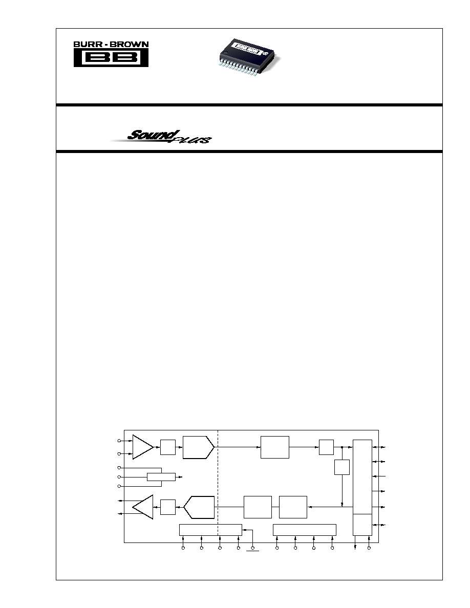
PCM3500
Interpolation
Digital Filter
Mode Control
Decimation
Digital Filter
Reference
AAF
HPF
M/S
HPFD
TSC
XTI
XTO
LOOP
V
REF
1
V
COM
V
REF
2
V
IN
AGND
Serial I/O Interface
PDWN
Power
DGND
AGND
V
DD
V
CC
Loop
FS
BCK
DIN
DOUT
FSO
SCKIO
Clock
Gen/
OSC
Modulator
(ADC)
Modulator
SMF
V
OUT
AGND
Multi-Level
DAC
q
POWER SUPPLY: Single +2.7V to +3.6V
q
SMALL PACKAGE: SSOP-24
For most current data sheet and other product
information, visit www.burr-brown.com
SBAS117

Æ
2
PCM3500
SPECIFICATIONS
All specifications at +25
∞
C, V
DD
= V
CC
= 3.3V, f
S
= 8kHz, and nominal system clock (XTI) = 512f
S
, unless otherwise noted. Measurement band is 100Hz to 0.425f
S
.
NOTES: (1) Pins 6, 7, 8, 9, 10, 15, 17, 18, 19, 20 (M/S, TSC, BCK, FS, DIN, SCKIO, XTI, HPFD, LOOP, PDWN). (2) Pins 8, 9, 10, 15, 17 (BCK, FS, DIN, SCKIO
(Schmitt-Trigger input) XTI. (3) Pins 6, 7, 18, 19, 20 (M/S, TSC, HPFD, LOOP, PDWN; Schmitt-Trigger input with internal pull-down). (4) Pins 8, 9, 11, 12, 15,
16 (BCK, FS, DOUT, FSO, SCKIO, XTO).
PCM3500E
PARAMETER
CONDITIONS
MIN
TYP
MAX
UNITS
RESOLUTION
16
Bits
DATA FORMAT
Serial Data Interface Format
DSP Format
Serial Data Bit Length
16
Bits
Serial Data Format
Sampling Frequency, f
S
ADC and DAC
7.2
8
26
kHz
System Clock Frequency, 512f
S
3.686
4.096
13.312
MHz
DIGITAL INPUT/OUTPUT
Logic Family
CMOS
Input Logic Level: V
IH
(1)
0.7 ∑ V
DD
VDC
V
IL
(1)
0.3 ∑ V
DD
VDC
Input Logic Current: I
IN
(2)
±
1
µ
A
I
IN
(3)
100
µ
A
Output Logic Level: V
OH
(4)
I
OUT
= ≠1mA
V
DD
≠ 0.3
VDC
V
OL
(4)
I
OUT
= +1mA
0.3
VDC
ADC CHARACTERISTICS
DC ACCURACY
Input Voltage
0.6 V
CC
Vp-p
Gain Error
±
2
±
5
% of FSR
Offset Error
High-Pass Filter Disabled
±
2
% of FSR
Input Resistance
50
k
AC ACCURACY
THD+N
f
IN
= 1kHz, V
IN
= ≠0.5dB
≠85
≠80
dB
Dynamic Range
Without A-Weighting
82
88
dB
Signal-to-Noise Ratio
Without A-Weighting
82
88
dB
Crosstalk
DAC Channel Idle, 0dB Input
80
85
dB
Passband Ripple (internal HPF enabled)
0.0002f
S
to 0.425f
S
±
0.05
dB
Passband Ripple (internal HPF disabled)
0f
S
to 0.425f
S
±
0.05
dB
Roll-Off at 0.00002f
S
High-Pass Filter Enabled
≠3
dB
Roll-Off at 0.56f
S
High-Pass Filter Enabled
≠30
dB
Stopband Rejection
0.58f
S
to f
S
≠65
dB
Group Delay
18/f
S
4m
sec
DAC CHARACTERISTICS
DC ACCURACY
Output Voltage
0.6 V
CC
Vp-p
Gain Error
±
1
±
5
% of FSR
Offset Error
High Pass Filter Disabled
±
1
% of FSR
Load Resistance
10
k
AC ACCURACY
THD+N
f
IN
= 1kHz, V
OUT
= 0dB
≠90
≠82
dB
Dynamic Range
Without A-Weighted
84
92
dB
Signal-to-Noise Ratio
Without A-Weighted
84
92
dB
Crosstalk
ADC Channel Idle, 0dB Input
84
92
dB
Passband Ripple
0f
S
to 0.425f
S
±
0.4
dB
Group Delay
12/f
S
4m
sec
POWER SUPPLY REQUIREMENTS
Voltage Range
V
CC
, V
DD
2.7
3.3
3.6
VDC
Supply Current, I
CC
+ I
DD
V
CC
= 3.3V
9
12
mA
Total Supply Current in Power-Down Mode
V
CC
= V
DD
= 3.3V, XTI Stopped
60
µ
A
Total Power Dissipation
V
CC
= V
DD
= 3.3V
30
40
mW
TEMPERATURE RANGE
Operating
≠25
+85
∞
C
Storage
≠55
+125
∞
C
Thermal Resistance,
JA
100
∞
C/W
MSB-First, Binary Two's Complement
Æ
3
PCM3500
The information provided herein is believed to be reliable; however, BURR-BROWN assumes no responsibility for inaccuracies or omissions. BURR-BROWN assumes no
responsibility for the use of this information, and all use of such information shall be entirely at the user's own risk. Prices and specifications are subject to change without notice.
No patent rights or licenses to any of the circuits described herein are implied or granted to any third party. BURR-BROWN does not authorize or warrant any BURR-BROWN
product for use in life support devices and/or systems.
Supply Voltage, +V
DD
, +V
CC
............................................................. +6.5V
Supply Voltage Differences ...............................................................
±
0.1V
GND Voltage Differences ..................................................................
±
0.1V
Digital Input Voltage ................................................... ≠0.3V to V
DD
+ 0.3V
Input Current (any pins except supply) ...........................................
±
10mA
Power Dissipation .......................................................................... 300mW
Operating Temperature Range ......................................... ≠25
∞
C to +85
∞
C
Storage Temperature ...................................................... ≠55
∞
C to +125
∞
C
Junction Temperature ...................................................................... 150
∞
C
Lead Temperature (soldering, 5s) .................................................. +260
∞
C
(reflow, 10s) ................................................................................ +235
∞
C
ABSOLUTE MAXIMUM RATINGS
ELECTROSTATIC
DISCHARGE SENSITIVITY
This integrated circuit can be damaged by ESD. Burr-Brown
recommends that all integrated circuits be handled with
appropriate precautions. Failure to observe proper handling
and installation procedures can cause damage.
ESD damage can range from subtle performance degrada-
tion to complete device failure. Precision integrated circuits
may be more susceptible to damage because very small
parametric changes could cause the device not to meet its
published specifications.
PACKAGE
SPECIFIED
DRAWING
TEMPERATURE
PACKAGE
ORDERING
TRANSPORT
PRODUCT
PACKAGE
NUMBER
RANGE
MARKING
NUMBER
(1)
MEDIA
PCM3500E
24-Lead SSOP
338
≠25
∞
C to +85
∞
C
PCM3500E
PCM3500E
Rails
"
"
"
"
"
PCM3500E/2K
Tape and Reel
NOTES: (1) Models with a slash (/) are available only in Tape and Reel in the quantities indicated (e.g., /2K indicates 2000 devices per reel). Ordering 2,000 pieces
of "PCM3500E/2K" will get a single 2000-piece Tape and Reel.
PACKAGE/ORDERING INFORMATION
Æ
4
PCM3500
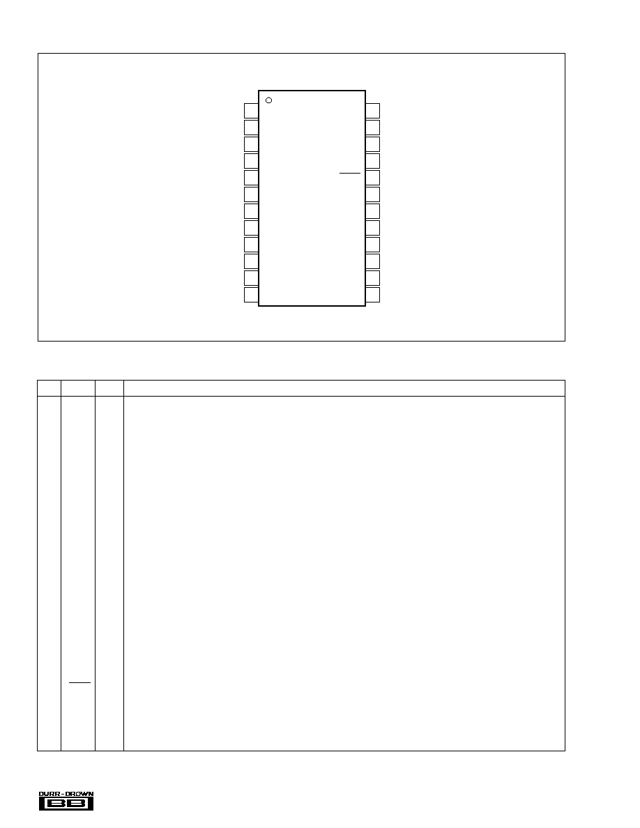
PIN CONFIGURATION
Top View
SSOP
PIN
NAME
I/O
DESCRIPTION
1
V
COM
OUT
Common-Mode Voltage (0.5V
CC)
. This pin should be connected to ground through a capacitor.
2
V
REF
1
--
Decouple Pin for Reference Voltage 1 (0.99V
CC
). This pin should be connected to ground through a capacitor.
3
V
REF
2
--
Decouple Pin for Reference Voltage 2 (0.2V
CC
). This pin should be connected to ground through a capacitor.
4
V
IN
IN
Analog Input for the ADC.
5
AGND
--
Analog Ground for the ADC Input Signal.
6
M/S
IN
Master/Slave Select. This pin is used to determine the operating mode for the serial interface. A logic `0' on this pin selects the Slave
Mode. A logic `1' on this pin selects the Master Mode.
(2)
7
TSC
IN
Time Slot Mode Control. This pin is used to select the time slot operating mode. A logic `0' on this pin disables Time Slot Mode. A
logic `1' on this pin enables Time Slot Mode.
(2)
8
BCK
I/O
Bit Clock. This pin serves as the bit (or shift) clock for the serial interface. This pin is an input in Slave Mode and an output in Master
Mode.
(1)
9
FS
I/O
Frame Sync. This pin serves as the frame synchronization clock for the serial interface. This pin is an input in Slave Mode and an
output in Master Mode.
(1)
10
DIN
IN
Serial Data Input. This pin is used to write 16-bit data to the DAC.
(1)
11
DOUT
OUT
Serial Data Output. The ADC outputs 16-bit data on this pin.
(3)
12
FSO
OUT
Frame Sync Output. Active only when Time Slot Mode is enabled. This pin is set to a high impedance state when Time Slot mode
is disabled (TSC = 0).
13
V
DD
--
Digital Power Supply. Used to power the digital section of the ADC and DAC, as well as the serial interface and mode control logic.
This pin is not internally connected to V
CC
.
14
DGND
--
Digital Ground. Internally connected through the substrate to analog ground.
15
SCKIO
I/O
System Clock Input/Output. This pin is a system clock output when using the crystal oscillator or XTI as the system clock input; when
XTI is connected to ground, this pin is a system clock input.
(1)
16
XTO
OUT
Crystal Oscillator Output.
17
XTI
IN
Crystal Oscillator Input or an External System Clock Input.
18
HPFD
IN
High-Pass Filter Disable. When this pin is set to a logic `1', the HPF function in the ADC is disabled.
(2)
19
LOOP
IN
ADC-to-DAC Loop-Back Control. When this pin is set to logic `1', the ADC data is fed to the DAC input.
(2)
20
PDWN
IN
Power Down and Reset Control. When this pin is logic `0', Power-Down Mode is enabled. The PCM3500 is reset on the rising edge
of this signal.
(2)
21
AGND
--
Analog Ground for the DAC Output Signal.
22
V
OUT
OUT
Analog Output from the DAC Output Filter.
23
AGND
--
Analog Ground. This is the ground for the internal analog circuitry.
24
V
CC
--
Analog Power Supply. Used to power the analog circuitry of the ADC and DAC.
NOTES: (1) Schmitt-Trigger input. (2) Schmitt-Trigger input with an internal pull-down resistor. (3) Tri-state output in Time Slot Mode.
PIN ASSIGNMENTS
V
COM
V
REF
1
V
REF
2
V
IN
AGND
M/S
TSC
BCK
FS
DIN
DOUT
FSO
V
CC
AGND
V
OUT
AGND
PDWN
LOOP
HPFD
XTI
XTO
SCKIO
DGND
V
DD
1
2
3
4
5
6
7
8
9
10
11
12
24
23
22
21
20
19
18
17
16
15
14
13
PCM3500
Æ
5
PCM3500
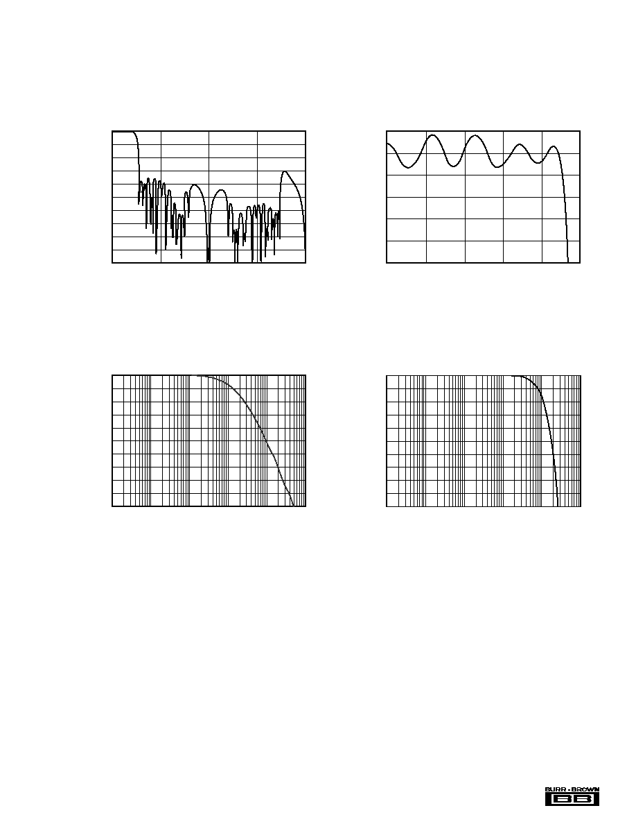
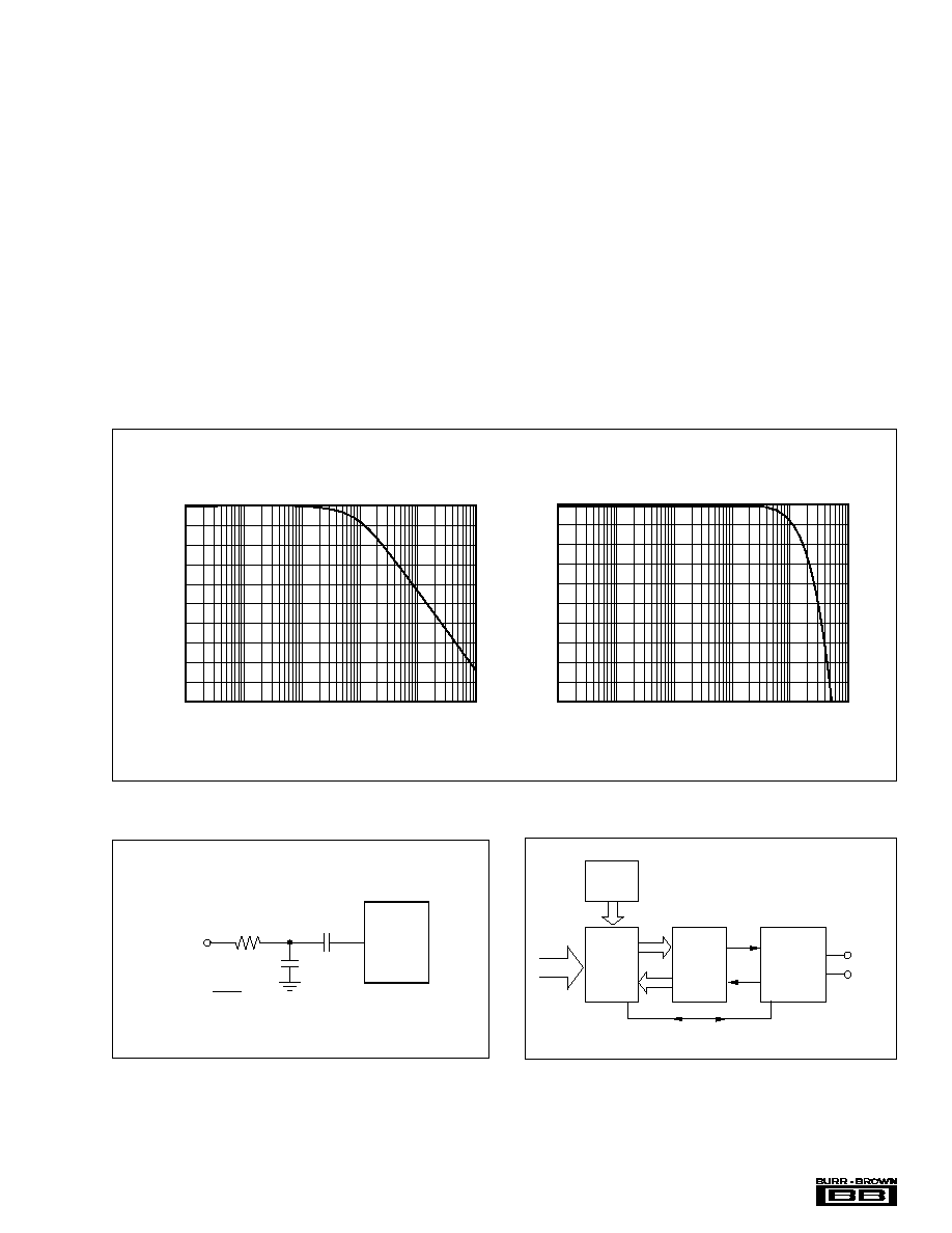
TYPICAL PERFORMANCE CURVES
INTERPOLATION FILTER
PASSBAND RIPPLE CHARACTERISTICS
0.2
0.0
≠0.2
≠0.4
≠0.6
≠0.8
≠1.0
0
0.1
0.2
0.3
0.4
0.5
Amplitude (dB)
Normalized Frequency (∑ f
S
Hz)
OUTPUT FILTER FREQUENCY RESPONSE
STOPBAND CHARACTERISTICS
Frequency (Hz)
Amplitude (dB)
0
≠10
≠20
≠30
≠40
≠50
≠60
≠70
≠80
≠90
≠100
100
1k
10k
100k
1M
10M
ANALOG FILTER
OUTPUT FILTER FREQUENCY RESPONSE
PASSBAND CHARACTERISTICS
Frequency (Hz)
Amplitude (dB)
0
≠1
≠2
≠3
≠4
≠5
≠6
≠7
≠8
≠9
≠10
100
10
1
1k
10k
100k
DAC SECTION
DIGITAL FILTER
Amplitude (dB)
INTERPOLATION FILTER FREQUENCY RESPONSE
Normalized Frequency (∑ f
S
)
0
≠10
≠20
≠30
≠40
≠50
≠60
≠70
≠80
≠90
≠100
0
1
2
3
4

Æ
6
PCM3500
TYPICAL PERFORMANCE CURVES
(Cont.)
T
A
= +25
∞
C, V
CC
= V
DD
= +3.3V, f
S
= 8kHz, and f
SIGNAL
= 1kHz, unless otherwise specified.
DAC OUTPUT SPECTRUM (≠0dB, N = 8192)
Frequency (kHz)
Amplitude (dB)
0
≠20
≠40
≠60
≠80
≠100
≠120
≠140
1
2
3
4
0
DAC OUTPUT SPECTRUM (≠60dB, N = 8192)
Frequency (kHz)
Amplitude (dB)
0
≠20
≠40
≠60
≠80
≠100
≠120
≠140
1
2
3
4
0
TOTAL HARMONIC DISTORTION + NOISE
vs SIGNAL NOISE
Signal Level (dB)
THD+N (dB)
0
≠20
≠40
≠60
≠80
≠100
≠84
≠72
≠60
≠48
≠36
≠24
≠12
0
≠96
THD+N fluctuates with signal level
as harmonics are limited to second
and third components.
DAC OUT-OF-BAND NOISE SPECTRUM
(BPZ, N = 2048)
Frequency (kHz)
Amplitude (dB)
0
≠20
≠40
≠60
≠80
≠100
≠120
≠140
8
16
24
32
40
48
56
64
0
DAC SECTION
DAC OUTPUT SPECTRA
Æ
7
PCM3500
TYPICAL PERFORMANCE CURVES
(Cont.)
THD+N at ≠0dB (dB)
TOTAL HARMONIC DISTORTION + NOISE
vs TEMPERATURE
(T
A
= ≠25
∞
C to +85
∞
C)
Temperature (
∞
C)
≠88
≠90
≠92
≠94
≠96
≠25
0
25
50
75
100
≠50
Dynamic Range and SNR (dB)
DYNAMIC RANGE AND SIGNAL-TO-NOISE RATIO
vs TEMPERATURE
(T
A
= ≠25
∞
C to +85
∞
C)
Temperature (
∞
C)
96
94
92
90
88
≠25
0
25
50
75
100
≠50
Dynamic Range
SNR
THD+N at ≠0dB (dB)
TOTAL HARMONIC DISTORTION + NOISE
vs SUPPLY VOLTAGE
(V
CC
= V
DD
= +2.7V to +3.6V)
Supply Voltage (V)
≠88
≠90
≠92
≠94
≠96
2.7
3.0
3.3
3.6
3.9
2.4
Dynamic Range and SNR (dB)
DYNAMIC RANGE AND SIGNAL-TO-NOISE RATIO
vs SUPPLY VOLTAGE
(V
CC
= V
DD
= +2.7V to +3.6V)
Supply Voltage (V)
96
94
92
90
88
2.7
3.0
3.3
3.6
3.9
2.4
Dynamic Range
SNR
THD+N at ≠0dB (dB)
TOTAL HARMONIC DISTORTION + NOISE
vs SAMPLING FREQUENCY
(f
S
= 8kHz to 26kHz)
f
S
(kHz)
≠88
≠90
≠92
≠94
≠96
8
16
24
32
0
BW = 3.4kHz
Dynamic Range and SNR (dB)
DYNAMIC RANGE AND SIGNAL-TO-NOISE RATIO
vs SAMPLING FREQUENCY
(f
S
= 8kHz to 26kHz)
f
S
(kHz)
96
94
92
90
88
8
16
24
32
0
BW = 3.4kHz
Dynamic Range
SNR
DAC SECTION
DAC CHARACTERISTICS vs TEMPERATURE, SUPPLY, AND SAMPLING FREQUENCY
Æ
8
PCM3500
TYPICAL PERFORMANCE CURVES
ADC SECTION
DIGITAL FILTER
DECIMATION FILTER FREQUENCY RESPONSE
Normalized Frequency (∑ f
S
Hz)
Amplitude (dB)
0
≠20
≠40
≠60
≠80
≠100
≠120
≠140
≠160
≠180
≠200
8
16
24
32
0
DECIMATION FILTER
STOPBAND ATTENUATION CHARACTERISTICS
Normalized Frequency (∑ f
S
Hz)
Amplitude (dB)
0
≠10
≠20
≠30
≠40
≠50
≠60
≠70
≠80
≠90
≠100
0.2
0.4
0.6
0.8
1.0
0
DECIMATION FILTER
PASSBAND RIPPLE CHARACTERISTICS
Normalized Frequency (∑ f
S
Hz)
Amplitude (dB)
0.2
0.0
≠0.2
≠0.4
≠0.6
≠0.8
≠1.0
0.1
0.2
0.3
0.4
0.5
0
DECIMATION FILTER TRANSITION
BAND CHARACTERISTICS
Normalized Frequency (∑ f
S
Hz)
Amplitude (dB)
0
≠1
≠2
≠3
≠4
≠5
≠6
≠7
≠8
≠9
≠10
0.45
0.46 0.47 0.48 0.49
0.50 0.51
0.52 0.53 0.54 0.55
≠4.13dB at 0.5 ∑ f
S
HIGH-PASS FILTER FREQUENCY RESPONSE
STOPBAND CHARACTERISTICS
Normalized Frequency (∑ f
S
/1000 Hz)
Amplitude (dB)
0
≠10
≠20
≠30
≠40
≠50
≠60
≠70
≠80
≠90
≠100
0.1
0.2
0.3
0.4
0.5
0
HIGH-PASS FILTER FREQUENCY RESPONSE
PASSBAND CHARACTERISTICS
Normalized Frequency (∑ f
S
/1000 Hz)
Amplitude (dB)
0.0
≠0.1
≠0.2
≠0.3
≠0.4
≠0.5
≠0.6
≠0.7
≠0.8
≠0.9
≠10
1
2
3
4
0
Æ
9
PCM3500
TYPICAL PERFORMANCE CURVES
(Cont.)
T
A
= +25
∞
C, V
CC
= V
DD
= +3.3V, f
S
= 8kHz, and f
SIGNAL
= 1kHz, unless otherwise specified.
ADC SECTION
ANALOG FILTER
ANTI-ALIASING FILTER
STOPBAND CHARACTERISTICS
Frequency (Hz)
Amplitude (dB)
0
≠5
≠10
≠15
≠20
≠25
≠30
≠35
≠40
≠45
≠50
1k
100
10k
100k
1M
10M
ANTI-ALIASING FILTER
PASSBAND CHARACTERISTICS
Frequency (Hz)
Amplitude (dB)
0
≠0.1
≠0.2
≠0.3
≠0.4
≠0.5
≠0.6
≠0.7
≠0.8
≠0.9
≠1.0
1k
100
10
1
10k
100k
ADC OUTPUT SPECTRUM (≠0.5dB, N = 8192)
Frequency (kHz)
Amplitude (dB)
0
≠20
≠40
≠60
≠80
≠100
≠120
≠140
1
2
3
4
0
ADC OUTPUT SPECTRA
ADC OUTPUT SPECTRUM (≠60dB, N = 8192)
Frequency (kHz)
Amplitude (dB)
0
≠20
≠40
≠60
≠80
≠100
≠120
≠140
1
2
3
4
0
TOTAL HARMONIC DISTORTION + NOISE
vs SIGNAL NOISE
Signal Level (dB)
THD+N (dB)
0
≠20
≠40
≠60
≠80
≠100
≠84
≠72
≠60
≠48
≠36
≠24
≠12
0
≠96
THD+N fluctuates with signal level
as harmonics are limited to second
and third components.

Æ
10
PCM3500
TYPICAL PERFORMANCE CURVES
(Cont.)
T
A
= +25
∞
C, V
CC
= V
DD
= +3.3V, f
S
= 8kHz, and f
SIGNAL
= 1kHz, unless otherwise specified.
ADC SECTION
ADC CHARACTERISTICS vs TEMPERATURE, SUPPLY AND SAMPLING FREQUENCY
THD+N at ≠0.5dB (dB)
TOTAL HARMONIC DISTORTION + NOISE
vs TEMPERATURE
(T
A
= ≠25
∞
C to +85
∞
C)
Temperature (
∞
C)
≠84
≠86
≠88
≠90
≠92
≠25
0
25
50
75
100
≠50
Dynamic Range and SNR (dB)
DYNAMIC RANGE AND SIGNAL-TO-NOISE RATIO
vs TEMPERATURE
(T
A
= ≠25
∞
C to +85
∞
C)
Temperature (
∞
C)
92
90
88
86
84
≠25
0
25
50
75
100
≠50
Dynamic Range
SNR
THD+N at ≠0.5dB (dB)
TOTAL HARMONIC DISTORTION + NOISE
vs SUPPLY VOLTAGE
(V
CC
= V
DD
= +2.7V to +3.6V)
Supply Voltage (V)
≠84
≠86
≠88
≠90
≠92
2.7
3.0
3.3
3.6
3.9
2.4
Dynamic Range and SNR (dB)
DYNAMIC RANGE AND SIGNAL-TO-NOISE RATIO
vs SUPPLY VOLTAGE
(V
CC
= V
DD
= +2.7V to +3.6V)
Supply Voltage (V)
92
90
88
86
84
2.7
3.0
3.3
3.6
3.9
2.4
SNR
Dynamic Range
THD+N at ≠0.5dB (dB)
TOTAL HARMONIC DISTORTION + NOISE
vs SAMPLING FREQUENCY
(f
S
= 8kHz to 26kHz)
f
S
(kHz)
≠84
≠86
≠88
≠90
≠92
8
16
24
32
0
BW = 3.4kHz
Dynamic Range and SNR (dB)
DYNAMIC RANGE AND SIGNAL-TO-NOISE RATIO
vs SAMPLING FREQUENCY
(f
S
= 8kHz to 26kHz)
f
S
(kHz)
96
94
92
90
88
8
16
24
32
0
BW = 3.4kHz
Dynamic Range
SNR

Æ
11
PCM3500
I
CC
, I
DD
and I
CC
+ I
DD
(mA)
SUPPLY CURRENT vs SUPPLY VOLTAGE
Supply Voltage (V)
12
10
8
6
4
2
0
2.7
3.0
3.3
3.6
3.9
2.4
I
CC
+ I
DD
I
CC
+ I
DD
at Power Down
I
CC
I
DD
SUPPLY CURRENT vs SUPPLY VOLTAGE AND SAMPLING FREQUENCY
I
CC
, I
DD
and I
CC
+ I
DD
(mA)
SUPPLY CURRENT vs SUPPLY VOLTAGE
Supply Voltage (V)
12
10
8
6
4
2
0
2.7
3.0
3.3
3.6
3.9
2.4
I
CC
+ I
DD
I
CC
+ I
DD
at Power Down
I
CC
I
DD
TYPICAL PERFORMANCE CURVES
(Cont.)
T
A
= +25
∞
C, V
CC
= V
DD
= +3.3V, f
S
= 8kHz, and f
SIGNAL
= 1kHz, unless otherwise specified.
Æ
12
PCM3500
SYSTEM CLOCK AND RESET/
POWER DOWN
SYSTEM CLOCK INPUT AND OUTPUT
The PCM3500 requires a system clock for operating the
digital filters and delta-sigma data converters.
The system clock may be supplied from an external master
clock or generated using the on-chip crystal oscillator cir-
cuit. Figure 1 shows the required connections for external
and crystal clock operation. The system clock must operate
at 512 times the sampling frequency, f
S
, with sampling
frequencies from 7.2kHz to 26kHz. This gives an effective
system clock frequency range of 3.6864MHz to 13.312MHz.
Table I shows system clock frequencies for common sam-
pling frequencies.
For external clock operation, XTI (pin 17) or SCKIO (pin 15)
is driven by a master clock source. If SCKIO is used as the
system clock input, then XTI must be connected to ground.
SAMPLING FREQUENCY (kHz)
SYSTEM CLOCK FREQUENCY (MHz)
8
4.096
11.025
5.6448
16
8.192
22.05
11.2896
24
12.288
TABLE I. System Clock Frequencies for Common Sam-
pling Frequencies.
FIGURE 1. System Clock Generation.
For either case, XTO (pin 16) should be left open. The system
clock source should be free of noise and exhibit low phase
jitter in order to obtain optimal dynamic performance from
the PCM3500. Figure 2 shows the system clock timing
requirements associated with an external master clock.
For crystal oscillator operation, a crystal is connected be-
tween XTI (pin 17) and XTO (pin 16), along with the
necessary load capacitors (10pF to 33pF per pin, as shown
in Figure 1). A fundamental-mode, parallel resonant crystal
is required.
FIGURE 2. External System Clock Timing Requirements.
C
1
C
2
C
1
, C
2
= 10pF to 33pF
XTI
R
Crystal
XTO
PCM3500
SCKIO
CRYSTAL RESONATOR
CONNECTION
External
Clock
External
Clock
XTI
XTO
R
PCM3500
EXTERNAL CLOCK INPUT-XTI
(XTO must be open)
SCKIO
XTI
XTO
R
PCM3500
EXTERNAL CLOCK INPUT-SCKIO
(XTO must be open)
SCKIO
System Clock Pulse Width HIGH t
CLKIH
20ns (min)
System Clock Pulse Width LOW
t
CLKIL
20ns (min)
t
CLKIH
t
CLKIL
1/512f
S
0.7V
DD
"H"
XTI
or
SCKIO
"L"
0.3V
DD
Æ
13
PCM3500
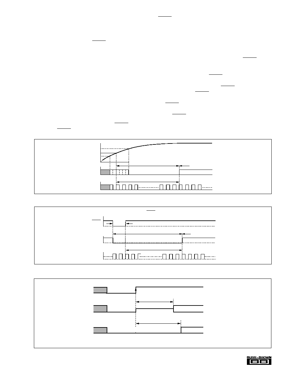
Reset and Power Down
The PCM3500 supports power-on reset, external reset, and
power-down operations. Power-on reset is performed by
internal circuitry automatically at power up, while the exter-
nal reset is initiated using the PDWN input (pin 20).
Power-on reset occurs when power and system clock are
initially applied to the PCM3500. The internal reset cir-
cuitry requires that the system clock be active at power up,
with at least three system clock cycles occurring prior to
V
DD
= 2.2V. When V
DD
exceeds 2.2V, the power-on reset
comparator enables the initialization sequence, which re-
quires 1024 system clock periods for completion. During
the initialization sequence, the DAC output is forced to
AGND, and the ADC output is forced to a high impedance
state. After the initialization sequence has completed, the
DAC and ADC outputs experience a delay before they
output a valid signal or data. Refer to Figures 3 and 5 for
power-on reset and post-reset delay timing.
External reset is performed by first setting PDWN = `0' and
then setting PDWN = `1'. The LOW to HIGH transition on
PDWN causes the reset initialization sequence to start.
During the initialization sequence, the DAC output is forced
to AGND, and the ADC output is forced to a high impedance
state. After the initialization sequence has completed, the
DAC and ADC outputs experience a delay before they
output a valid signal or data. Refer to Figures 4 and 5 for
external reset and post-reset delay timing.
Power-down mode is enabled by setting PDWN = `0'.
During power-down mode, minimum current is drawn when
the system clock is removed, resulting in 60
µ
A (typical)
power supply current. The PDWN input includes an internal
pull-down resistor, which places the PCM3500 in power-
down mode at power-up if the PDWN pin is left uncon-
nected. Ideally, the PDWN input should be driven by active
logic in order to control reset and power-down operation. If
the PDWN pin is to be unused in the system application, it
should be connected to V
DD
to enable normal operation. By
setting PDWN = `1' when exiting power-down mode, the
PCM3500 will initiate an external reset as described earlier
in this section.
1024 System Clock Periods
Reset
Reset Removal
2.4V
2.2V
2.0V
V
DD
Internal Reset
System Clock
FIGURE 3. Power-On Reset Timing.
1024 System Clock Periods
Reset
Reset Removal
System Clock
Internal Reset
PDWN
t
RST
PWDN = LOW Pulse Width
t
RST
= 40ns minimum
FIGURE 4. External Reset Timing.
FIGURE 5. DAC and ADC Output for Reset and Power Down.
Reset
Power Down
GND
V
COM
(0.5V
CC
)
Ready/Operation
Internal Reset
or Power Down
ADC DOUT
DAC V
OUT
High Impedance
(1)
t
ADCDLY1
(2304/f
S
)
t
DACDLY1
(2048/f
S
)
Reset Removal or Power Down OFF
NOTE: (1) The HPF transient response (exponentially attenuated signal from
±
0.2% DC of FSR with 200ms time constant) appears initially.
Æ
14
PCM3500
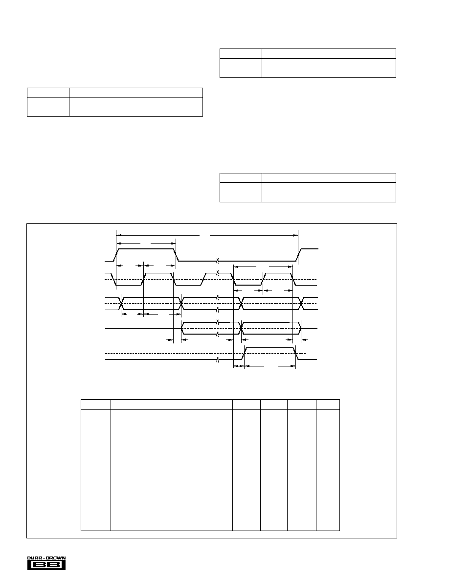
SERIAL INTERFACE
The serial interface of the PCM3500 is a 4-wire synchronous
serial port. It includes FS (pin 9), BCK (pin 8), DIN (pin 10)
and DOUT (pin 11). FS is the frame synchronization clock,
BCK is the serial bit or shift clock, DIN is the serial data input
for the DAC, and DOUT is the serial data output for the ADC.
The frame sync, FS, operates at the sampling frequency (f
S
).
The bit clock, BCK, operates at 16f
S
for normal operation.
DIN and DOUT also operate at the bit clock rate. Both FS
and BCK must be synchronous with the system clock (guar-
anteed in Master Mode). Data for DIN is clocked into the
serial interface on the rising edge of BCK, while data for
DOUT is clocked out of the serial interface on the falling
edge of BCK.
Figure 6 shows the serial interface format for the PCM3500.
The serial data for DIN and DOUT must be in Binary Two's
Complement, MSB-first format. Figures 7 and 8 show the
timing specifications for the serial interface when used in
Slave and Master Modes.
FS
BCK
DIN
DOUT
MSB
MSB
LSB
LSB
MSB
MSB
LSB
LSB
15 14 13 12 11
2
1
0
5
4
3
15 14 13 12 11
2
1
0
5
4
3
15 14 13 12 11
2
1
0
5
4
3
15 14 13 12 11
2
1
0
5
4
3
1/f
S
16-Bit/Frame
SYMBOL
DESCRIPTION
MIN
TYP
MAX
UNITS
t
BCKP
BCK Period
2400
ns
t
BCKH
BCK Pulse Width HIGH
800
ns
t
BCKL
BCK Pulse Width LOW
800
ns
t
FSW
FS Pulse Width HIGH
t
BCKP
≠ 60
t
BCKP
t
BCKP
+ 60
ns
t
FSP
FS Period
1/f
S
t
FSSU
FS Set Up Time to BCK Rising Edge
60
ns
t
FSHD
FS Hold Time to BCK Rising Edge
60
ns
t
DISU
DIN Set Up Time to BCK Rising Edge
60
ns
t
DIHD
DIN Hold Time to BCK Rising Edge
60
ns
t
CKDO
Delay Time BCK Falling Edge to DOUT
0
80
ns
t
R
Rising Time of All Signals
30
ns
t
F
Falling Time of All Signals
30
ns
FIGURE 6. Serial Interface Format.
FIGURE 7. Serial Interface Timing for Slave Mode.
t
FSW
t
FSSU
t
FSHD
t
BCKP
t
BCKH
t
DISU
t
DIHD
t
BCKL
t
CKDO
t
FSP
FS
(input)
BCK
(input)
DIN
(input)
DOUT
(output)
NOTES: Timing measurement reference level is (VIH/VIL)/2. RIsing and falling time is measured
from 10% to 90% of IN/OUT signal swing. Load capacitance of DOUT signal is 50pF.
0.5V
DD
0.5V
DD
0.5V
DD
0.5V
DD
Æ
15
PCM3500
SERIAL
INTERFACE
M/S (PIN 6)
MODE
FS (PIN)
BCK (PIN 8)
0
Slave
Input
Input
1
Master
Output
Output
TABLE II. Master/Slave Mode Selection.
SYMBOL
DESCRIPTION
MIN
TYP
MAX
UNITS
t
BCKP
BCK Period
2400
16000
ns
t
BCKH
BCK Pulse Width HIGH
1200
8000
ns
t
BCKL
BCK Pulse Width LOW
1200
8000
ns
t
CKFS
Delay Time BCK Falling Edge to FS
≠ 40
40
ns
t
FSW
FS Pulse Width HIGH
t
BCKP
≠ 60
t
BCKP
t
BCKP
+ 60
ns
t
FSP
FS Period
1/f
S
t
DISU
DIN Set Up Time to BCK Rising Edge
60
ns
t
DIHD
DIN Hold Time to BCK Rising Edge
60
ns
t
CKDO
Delay Time BCK Falling Edge to DOUT
0
80
ns
t
R
Rising Time of All Signals
30
ns
t
F
Falling Time of All Signals
30
ns
FIGURE 8. Serial Interface Timing for Master Mode.
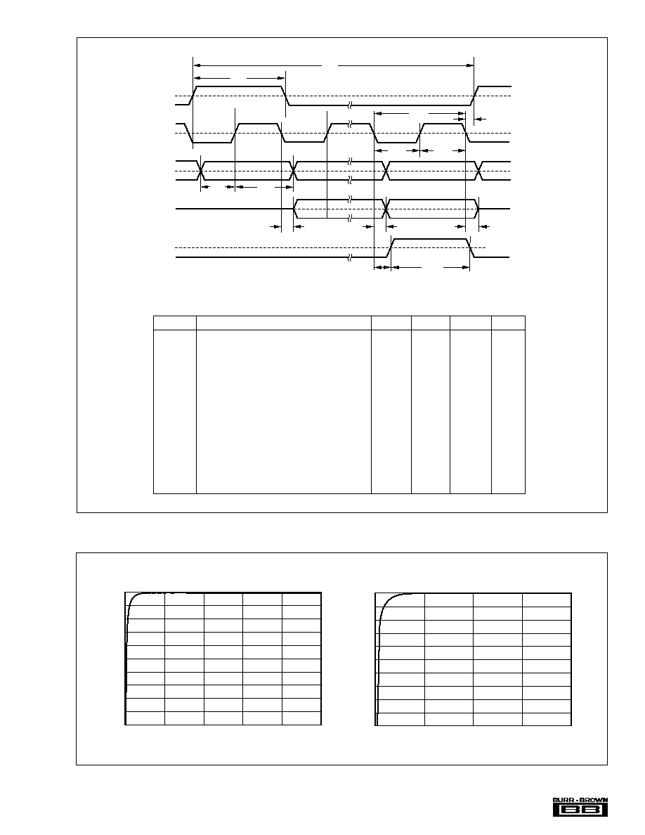
MASTER/SLAVE OPERATION
The serial interface supports both Slave and Master Mode
operation. The mode is selected by the M/S input (pin 6).
Table II shows mode and pin settings corresponding to the
M/S input selection. Figure 9 shows connections for Slave
and Master mode operation.
FIGURE 9. Slave and Master Mode Connections.
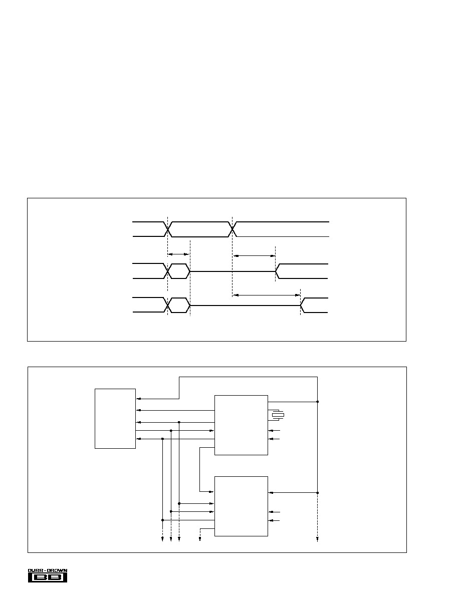
Slave Mode Operation
In Slave Mode, the FS and BCK pins are inputs to the
PCM3500. Both FS and BCK should be derived from the
system clock signal (XTI or SCKIO) to ensure proper
synchronization. Slave Mode is best suited for applications
where the DSP or controller is capable of generating the FS,
BCK, and system clocks using an on-chip serial port and/or
timing generator.
Master Mode Operation
In Master Mode operation, both FS and BCK are clock
outputs generated by the PCM3500 from the system clock
input (XTI, SCKIO, or a crystal). In Master Mode, the timing
and phase relationships between system clock, FS, and BCK
are managed internally to provide optimal synchronization.
XTI
FS
BCK
DIN
DOUT
M/S
TSC
GND
GND
Controller
System
Clock
Slave Mode
PCM3500
XTI
FS
BCK
DIN
DOUT
M/S
TSC
V
DD
GND
PCM3500
System
Clock
Controller
Master Mode
t
FSW
t
CKFS
t
BCKP
t
BCKH
t
DISU
t
DIHD
t
BCKL
t
CKDO
t
FSP
NOTES: Timing measurement reference level is (VIH/VIL)/2. Rising and falling time is measured from
10% to 90% of IN/OUT signal swing. Load capacitance of DOUT, FS, BCK signal is 50pF.
0.5V
DD
0.5V
DD
0.5V
DD
0.5V
DD
FS
(output)
BCK
(output)
DIN
(input)
DOUT
(output)
Æ
16
PCM3500
SYNCHRONIZATION REQUIREMENTS
The PCM3500 requires that FS and BCK be synchronous
with the system clock. Internal circuitry is included to detect
a loss of synchronization between FS and the system clock
input. If the phase relationship between FS and the system
clock varies more than
±
1.5 BCK periods, the PCM3500
will detect a loss of synchronization. Upon detection, the
DAC output is forced to 0.5V
CC
and the DOUT pin is forced
to a high impedance state. This occurs within one sampling
clock (FS) period of initial detection. Figure 10 shows the
loss of synchronization operation and the DAC and ADC
output delays associated with it.
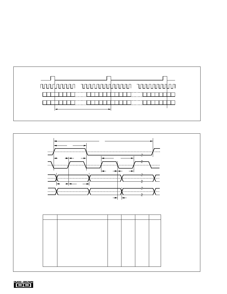
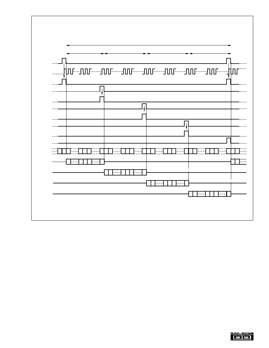
TIME SLOT OPERATION
The PCM3500 serial interface supports Time Division
Multiplexing (TDM) using the Time Slot Mode. Up to four
PCM3500s may be connected on the same 4-wire serial
interface bus. This is useful for system applications that
require multiple modem or voice channels. Figure 11 shows
examples of Time Slot Mode connections.
Time Slot Mode defines a 64-bit long frame, composed of
four time slots. Each slot is 16 bits long and corresponds to
one of four CODECs. The FS pin on the first PCM3500
(CODEC A, Slot 0) is used as the master frame sync, and
operates at the sampling frequency, f
S
. The bit clock, BCK,
operates at 64f
S
. DIN and DOUT of each CODEC also
operate at 64f
S
. Figure 12 shows the operation of the Time
Slot Mode.
Time Slot operation is enabled or disabled using the TSC
input (pin 7). The state of the TSC pin is updated at power-
on reset, or on the rising edge of PWDN input (if using
external reset or power-down mode). A forced reset is
required when changing from Slave to Master Mode, or visa
versa, in real time.
FIGURE 10. Loss of Synchronization Operation and Timing.
FIGURE 11. Time Slot Mode Connections.
Synchronous
Asynchronous
Synchronization
Lost
Resynchronization
within
1/f
S
Synchronous
Normal
Normal
t
ADCDLY2
(32/f
S
)
t
DACDLY2
(32/f
S
)
V
COM
(0.5 V
CC
)
V
COM
(0.5 V
CC
)
State of
Synchronization
DAC V
OUT
Normal
Normal
(1)
High Impedance
ADC DOUT
NOTE: (1) The HPF transient response (exponentially attenuated signal from
±
0.2% DC of FSR
with 200ms time constant) appears initially.
Undefined Data
Undefined Data
V
DD
V
DD
Controller
GND
V
DD
SCKIO
XTI
XTO
FS
BCK
DIN
DOUT
FSO
M/S
TSC
PCM3500
(CODEC B, Slot 1)
PCM3500
(CODEC A, Slot 0)
To Two PCM3500s
SCKIO
XTI
XTO
FS
BCK
DIN
DOUT
FSO
M/S
TSC
Æ
17
PCM3500
FIGURE 12. Time Slot Mode Operation.
FS
BCK
FS (A)
FSO (A)
FS (B)
FS (C)
FSO (C)
FS (D)
FSO (D)
DIN
FSO (B)
DOUT (A)
DOUT (B)
DOUT (C)
DOUT (D)
MSB
LSB
High Impedance
High Impedance
High Impedance
High Impedance
High Impedance
Slot 0, 16 Bits
Slot 1, 16 Bits
Slot 2, 16 Bits
Slot 3, 16 Bits
CODEC A
CODEC B
One Frame = 1/f
S
, 64 Bits per Frame, 16 Bits per Slot
CODEC C
CODEC D
Æ
18
PCM3500
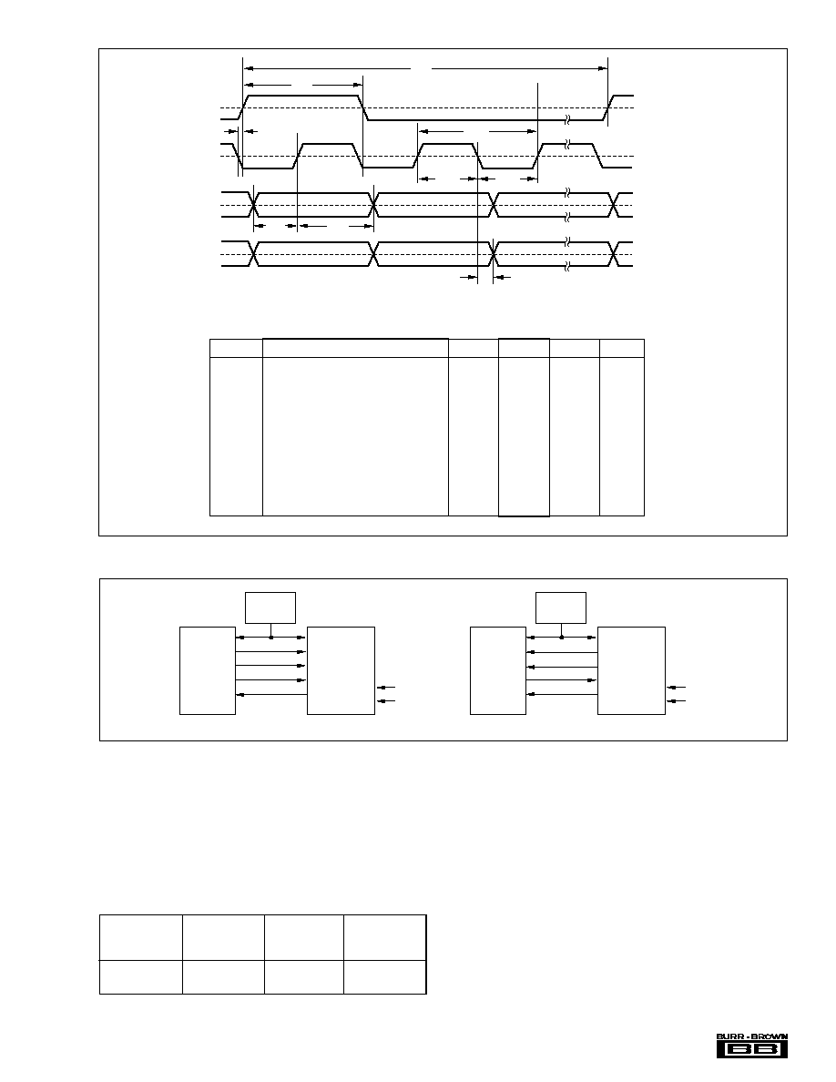
SYMBOL
DESCRIPTION
MIN
TYP
MAX
UNITS
t
BCKP
BCK Period
600
ns
t
BCKH
BCK Pulse Width HIGH
200
ns
t
BCKL
BCK Pulse Width LOW
200
ns
t
FSW
FS Pulse Width HIGH
t
BCKP
≠ 60
t
BCKP
t
BCKP
+ 60
ns
t
FSP
FS Period
1/f
S
t
FSSU
FS Set Up TIme to BCK Rising Edge
60
ns
t
FSHD
FS Hold TIme to BCK RIsing Edge
60
ns
t
DISU
DIN Set Up Time to BCK Rising Edge
60
ns
t
DIHD
DIN Hold Time to BCK Rising Edge
60
ns
t
CKDO
Delay Time BCK Falling Edge to DOUT
0
80
ns
t
HZDO
Delay Time BCK Falling Edge to DOUT Active
20
ns
t
DOHZ
Delay Time BCK Falling Edge to DOUT Inactive
19.5
ns
t
FSOW
FSO Pulse Width HIGH
t
BCKP
≠ 60
t
BCKP
t
BCKP
+ 60
ns
t
BFSO
Delay Time BCK Falling Edge to FSO
0
80
ns
t
R
Rising Time of All Signals
30
ns
t
F
Falling Time of All Signals
30
ns
FIGURE 13. Serial Interface Timing for Time Slot Mode Operation (Slave Mode).
Table III shows the TSC pin settings and corresponding
mode selections. When Time Slot Mode is enabled, FSO
(pin 12) is used as a frame sync output, which is connected
to the FS input of the next PCM3500 in the Time Slot
sequence. Figures 13 and 14 provide detailed timing for
Time Slot Mode operation.
TSC (PIN 7)
TIME SLOT MODE
0
Time Slot Mode Disabled, Normal Operation
1
Time Slot Operation Enable
LOOP (PIN 19)
LOOP-BACK MODE
0
Loop-Back Mode Disabled, Normal Operation
1
Loop-Back Mode Enabled
TABLE IV. Loop-Back Mode Selection.
TABLE III. Time Slot Mode Selection.
HPFD (PIN 18)
HIGH-PASS FILTER MODE
0
High-Pass Filter On
1
High-Pass Filter Off
TABLE V. High-Pass Filter Mode Selection.
HIGH-PASS FILTER
The PCM3500 includes a digital high-pass filter in the ADC
which may be used to remove the DC offset created by the
analog front-end (AFE) section. The high-pass filter response
is shown in Figure 15. The high-pass filter may be enabled or
disabled using the HPFD input (pin 18). Table V shows the
HPFD pin settings and corresponding mode selections.
ADC-TO-DAC LOOP BACK
The PCM3500 includes a Loop-Back Mode, which directly
feeds the ADC data to the DAC input. This mode is designed
for diagnostic testing and system adjustment. Loop-Back
Mode is enabled and disabled using the LOOP input (pin
19). Table IV shows the LOOP pin settings and correspond-
ing mode selections. The serial interface continues to oper-
ate in Loop-Back Mode, allowing the host to read the ADC
data at the DOUT pin.
t
FSW
t
FSSU
High Impedance
High Impedance
t
FSHD
t
BCKP
t
BCKL
t
DISU
t
DIHD
t
BCKH
t
CKDO
t
HZDO
t
DOHZ
t
FSP
NOTES: Timing measurement reference level is (VIH/VIL)/2. Rising and falling time is measured from
10% to 90% of IN/OUT signal swing. Load capacitance of DOUT, and FSO signal is 50pF.
0.5V
DD
0.5V
DD
0.5V
DD
0.5V
DD
0.5V
DD
t
FSOW
t
BFSO
FS
(input)
BCK
(input)
DIN
(input)
DOUT
(output)
FSO
(output)
Æ
19
PCM3500
SYMBOL
DESCRIPTION
MIN
TYP
MAX
UNITS
t
BCKP
BCK Period
600
4000
ns
t
BCKH
BCK Pulse Width HIGH
300
2000
ns
t
BCKL
BCK Pulse Width LOW
300
2000
ns
t
CKFS
Delay Time BCK Falling Edge to FS
≠40
40
ns
t
FSW
FS Pulse Width HIGH
t
BCKP
≠ 60
t
BCKP
t
BCKP
+ 60
ns
t
FSP
FS Period
1/f
S
t
DISU
DIN Set Up Time to BCK Rising Edge
60
ns
t
DIHD
DIN Hold Time to BCK Rising Edge
60
ns
t
CKDO
Delay Time BCK Falling Edge to DOUT
0
80
ns
t
HZDO
Delay Time BCK Falling Edge to DOUT Active
20
ns
t
DOHZ
Delay Time BCK Falling Edge to DOUT Inactive
19.5
ns
t
FSOW
FSO Pulse Width HIGH
t
BCKP
≠ 60
t
BCKP
t
BCKP
+ 60
ns
t
BFSO
Delay Time BCK Falling Edge to FSO
0
80
ns
t
R
Rising Time of All Signals
30
ns
t
F
Falling Time of All Signals
30
ns
FIGURE 14. Serial Interface Timing for Time Slot Mode Operation (Master Mode).
FIGURE 15. High-Pass Filter Response.
HIGH-PASS FILTER FREQUENCY RESPONSE
STOPBAND CHARACTERISTICS
Normalized Frequency (∑ f
S
/1000 Hz)
Amplitude (dB)
0
≠10
≠20
≠30
≠40
≠50
≠60
≠70
≠80
≠90
≠100
0.1
0.2
0.3
0.4
0.5
0
HIGH-PASS FILTER FREQUENCY RESPONSE
PASSBAND CHARACTERISTICS
Normalized Frequency (∑ f
S
/1000 Hz)
Amplitude (dB)
0.0
≠0.1
≠0.2
≠0.3
≠0.4
≠0.5
≠0.6
≠0.7
≠0.8
≠0.9
≠10
1
2
3
4
0
t
FSW
High Impedance
High Impedance
t
BCKP
t
CKFS
t
BCKL
t
DISU
t
DIHD
t
BCKH
t
CKDO
t
HZDO
t
DOHZ
t
FSP
NOTES: Timing measurement reference level is (VIH/VIL)/2. Rising and falling time is measured from
10% to 90% of IN/OUT signal swing. Load capacitance of DOUT, FSO, FS, and BCK signal is 50pF.
0.5V
DD
0.5V
DD
0.5V
DD
0.5V
DD
0.5V
DD
t
FSOW
t
BFSO
FS
(output)
BCK
(output)
DIN
(input)
DOUT
(output)
FSO
(output)

Æ
20
PCM3500
APPLICATIONS INFORMATION
BASIC CIRCUIT CONNECTIONS
The basic connection diagram for the PCM3500 is shown in
Figure 16. Included are the required power supply bypass and
reference decoupling capacitors. The DAC output, V
OUT
, and
the ADC input, V
IN
, should be AC-coupled to external cir-
cuitry.
Reference Pin Connections
The V
COM
voltage is used internally to bias the input and
output amplifier stages of the PCM3500. It is brought out
FIGURE 16. Basic Connection Diagram.
unbuffered on pin 1 for decoupling. A 1
µ
F to 10
µ
F alumi-
num electrolytic or tantalum capacitor is recommended for
decoupling purposes. This capacitor should be located as
close as possible to pin 1.
The V
COM
voltage is typically equal to V
CC
/2, and may be
used to bias external input and output circuitry. However,
since the V
COM
pin is not a buffered output, it must drive a
high impedance load to avoid excessive loading. Buffering
the V
COM
pin with an external op amp configured as a
voltage follower is recommended when driving multiple bias
nodes. Figure 17 shows examples of using V
COM
with
external circuitry.
FIGURE 17. Using V
COM
to Bias External Circuitry.
V
COM
V
REF
1
V
REF
2
V
IN
AGND
M/S
TSC
BCK
FS
DIN
DOUT
FSO
V
CC
AGND
V
OUT
AGND
PDWN
LOOP
HPFD
XTI
XTO
SCKIO
DGND
V
DD
1
2
3
4
5
6
7
8
9
10
11
12
24
23
22
21
20
19
18
17
16
15
14
13
PCM3500
+
+
+
+
C
3
C
4
C
5
C
6
Serial
Interface
+
+
C
1
+3.3V
External Reset
Power-Down Control
External Clock System
Analog Line Interface Circuit
Telecom Line
+
C
2
C
7
C
1
, C
2
: Power supply bypass capacitors. Parallel combination of a 1
µ
F to 10
µ
F aluminum electrolytic capacitor and 0.1
µ
F ceramic capacitor.
C
3
, C
4
, C
5
: V
REF
and V
COM
bypass capacitors. Use a 1
µ
F to 10
µ
F aluminum electrolytic capacitor.
C
6
, C
7
: Input/output AC-coupling capacitors. Use a 0.1
µ
F to 10
µ
F aluminum electrolytic capacitor.
+
V
OUT
Non-Polarized
1
µ
F
PCM3500
4.7
µ
F
V
COM
V
CC
PCM3500
OPA340
OPA343
+
4.7
µ
F
Use voltage follower
to buffer V
COM
To Bias
Nodes
V
COM
(a) Biasing an External Active Filter Stage
(b) Using a Buffer to Provide Bias for Multiple or
Low Input Impedance Nodes

Æ
21
PCM3500
V
REF
1 (pin 2) and V
REF
2 (pin 3) are reference voltages used
by the delta-sigma modulators. They are brought out strictly
for decoupling purposes. V
REF
1 and V
REF
2 are not to be
used to bias external circuits. A 1
µ
F to 10
µ
F aluminum
electrolytic or tantalum capacitor is recommended for
decoupling on each pin. These capacitors should be located
as close as possible to pins 2 and 3.
Power Supplies and Grounding
V
CC
(pin 24) and V
DD
(pin 13) should be connected directly
to the +2.7V to +3.6V analog power supply, as shown in
Figure 16. The AGNDs (pins 5, 21, and 23) and DGND (pin
14) should be connected directly to the analog ground.
Power supply bypass capacitors should be located as close
to the power supply pins as possible in order to ensure a low
impedance connection. A combination of a 10
µ
F aluminum
electrolytic or tantalum capacitor in parallel with a 0.1
µ
F
ceramic capacitor is recommended for both V
CC
and V
DD
.
V
DD
and V
CC
should not be connected to separate digital and
analog power supplies. This can lead to an SCR latch-up
condition, which can cause either degraded device perfor-
mance or catastrophic failures.
PCB LAYOUT GUIDELINES
The recommended PCB layout technique is shown in Figure
18. The analog and digital section of the board are separated
by a split ground plane, with the PCM3500 positioned
entirely over the analog section of the board. The AGNDs
(pins 5, 20, and 23) and DGND (pin 14) are connected
directly to the analog ground plane. The power supply pins,
V
CC
(pin 13) and V
DD
(pin 24), are routed directly to the
+2.7V to +3.6V analog power supply using wide copper
traces (100 mils or wider recommended) or a power plane.
Power supply bypass and reference decoupling capacitors
are shown located as close as possible to the PCM3500.
The PCM3500 is oriented so that the digital pins are facing
the ground plane split. Digital connections should be made
as short and direct as possible to limit high frequency
radiation and coupling. Series resistors (from 20
to 100
)
may be put in series with the system clock, FS, BCK, and
FSO lines to reduce or eliminate overshoot on clock edges,
further reducing radiated emissions. The split ground plane
should be connected at one point by a trace, wire, or ferrite
bead. Often the board will be designed to have several
jumper points for the common ground connection, so that
the best performance can be derived through experimenta-
tion.
An alternative technique, using a single power supply or
battery, is shown in Figure 19. This technique is more
suitable for portable applications.
FIGURE 18. Recommended PCB Layout Technique.
FIGURE 19. PCB Layout Using a Single-Supply or Battery.
PCM3500
V
CC
V
DD
AGND
Analog
Ground
Digital
Ground
DGND
Digital Power
Supply
Analog Power
Supply
+3.3V
Common
Connection
DIGITAL SECTION
ANALOG SECTION
Host
and
Logic
+3.3V
Digital I/Os
Split Grounds
PCM3500
V
CC
V
DD
AGND
Split Grounds
Ferrite
Beads
Analog
Ground
Digital
Ground
DGND
DIGITAL SECTION
ANALOG SECTION
Host
and
Logic
Common
Supply
Digital I/Os
Æ
22
PCM3500
OUTPUT FILTER CIRCUITS FOR THE DAC
The PCM3500's DAC uses delta-sigma conversion tech-
niques. It uses oversampling and noise shaping to improve
in-band (f = f
S
/2) signal-to-noise performance at the expense
of increased out-of-band noise. The DAC output must be
low-pass filtered to attenuate the out-of-band noise to a
reasonable level.
The PCM3500 includes a low-pass filter in the on-chip
output amplifier circuit. The frequency response for this
filter is shown in Figure 20. Although this filter helps to
lower the out-of-band noise, it is not adequate for many
applications. This is especially true for applications where
the sampling frequency is below 16kHz, since the out-of-
band noise above f
S
/2 is in the audio spectrum. An external
filter circuit, either passive or active, is required to provide
additional attenuation of the out-of-band noise. The low-
pass filter order will be dependent upon the out-of-band
noise requirements for a particular system. Generally, a 2nd-
order or better low-pass circuit will be required, with the
cut-off frequency set to f
S
/2 or less.
Burr-Brown Application Bulletin AB-034 provides infor-
mation for designing both Multiple Feedback and Sallen-
Key active filter circuits using software available from Burr-
Brown's web site. Another excellent reference for both
passive and active filter design is the "Electronic Filter
Design Handbook, Third Edition" by Williams and Taylor,
published by McGraw-Hill.
ON-CHIP ANALOG FRONT END FOR THE ADC
The PCM3500 A/D converter includes a fully differential
input delta-sigma modulator. In order to simplify connection
for single-ended applications, an analog front end (AFE)
circuit has been included on the PCM3500 just prior to the
modulator. The AFE circuit is shown in Figure 21.
FIGURE 20. DAC Output Amplifier Filter Response.
FIGURE 21. On-Chip AFE Circuit for the ADC.
50k
V
IN
4
1
2
3
V
COM
V
REF
1
V
REF
2
Delta-Sigma
Modulator
(+)
(≠)
Reference
+
+
1.0
µ
F
+
+
OUTPUT FILTER
STOPBAND FREQUENCY RESPONSE
Frequency (Hz)
Amplitude (dB)
0
≠10
≠20
≠30
≠40
≠50
≠60
≠70
≠80
≠90
≠100
100
1k
10k
100k
1M
10M
OUTPUT FILTER
PASSBAND FREQUENCY RESPONSE
Frequency (Hz)
Amplitude (dB)
0
≠1
≠2
≠3
≠4
≠5
≠6
≠7
≠8
≠9
≠10
100
10
1
1k
10k
100k
Æ
23
PCM3500
ANTI-ALIASING FILTER
STOPBAND CHARACTERISTICS
Frequency (Hz)
Amplitude (dB)
0
≠5
≠10
≠15
≠20
≠25
≠30
≠35
≠40
≠45
≠50
1k
100
10k
100k
1M
10M
ANTI-ALIASING FILTER
PASSBAND CHARACTERISTICS
Frequency (Hz)
Amplitude (dB)
0
≠0.1
≠0.2
≠0.3
≠0.4
≠0.5
≠0.6
≠0.7
≠0.8
≠0.9
≠1.0
1k
100
10
1
10k
100k
The AFE circuit consists of a single-ended-to-differential
converter, with the first stage of the circuit doubling as a
low-pass, anti-alias filter. The frequency response for the
filter is shown in Figure 22. Since the delta-sigma modulator
oversamples the input at 64f
S
, the anti-alias filter require-
ments are relaxed, with only a single-pole filter being re-
quired. If an application requires further band limiting of the
input signal, a simple RC filter at the V
IN
input (pin 4) can
be used, as shown in Figure 23.
SOFTWARE MODEM
APPLICATIONS
The PCM3500 was designed to meet the requirements for
software-based analog modems, supporting up to 56kbps
(1)
.
In a software modem application, the PCM3500 is paired
with a Data Access Arrangement (DAA) and a host CPU to
provide the complete modem function. Figure 24 shows a
simplified block diagram of a software modem using the
PCM3500.
The DAA provides the interface between the CODEC and
two-wire telephone line. The DAA provides numerous
functions, including two-to-four wire conversion, modem-
side to line-side isolation, ring detection, hook switch con-
trol, line current compensation, and overvoltage protection.
The host CPU provides the data pump and supervisory
functions for the software modem application. The host
executes modem software code, which includes the neces-
sary routines for transmit and receive functions, error detec-
tion and correction, echo cancellation, and CODEC/DAA
control and supervision.
NOTE: (1) Data transmission is limited to 53kbps over standard telephone
lines. Actual transmission rates vary depending upon the quality of the
lines and switching equipment for a given connection.
FIGURE 22. Anti-Alias Filter Frequency Response.
FIGURE 23. Optional External Low-Pass Filter for the
ADC.
FIGURE 24. Software Modem Block Diagram.
+
V
IN
PCM3500
Analog
Input
R
C
f
≠3dB
=
1
2
RC
Host
CPU
Controls (ring detect, off hook, etc.)
Modem
Software
PCM3500
CODEC
Data
Access
Arrangement
(DAA)
Data
Tip
Ring
Æ
24
PCM3500
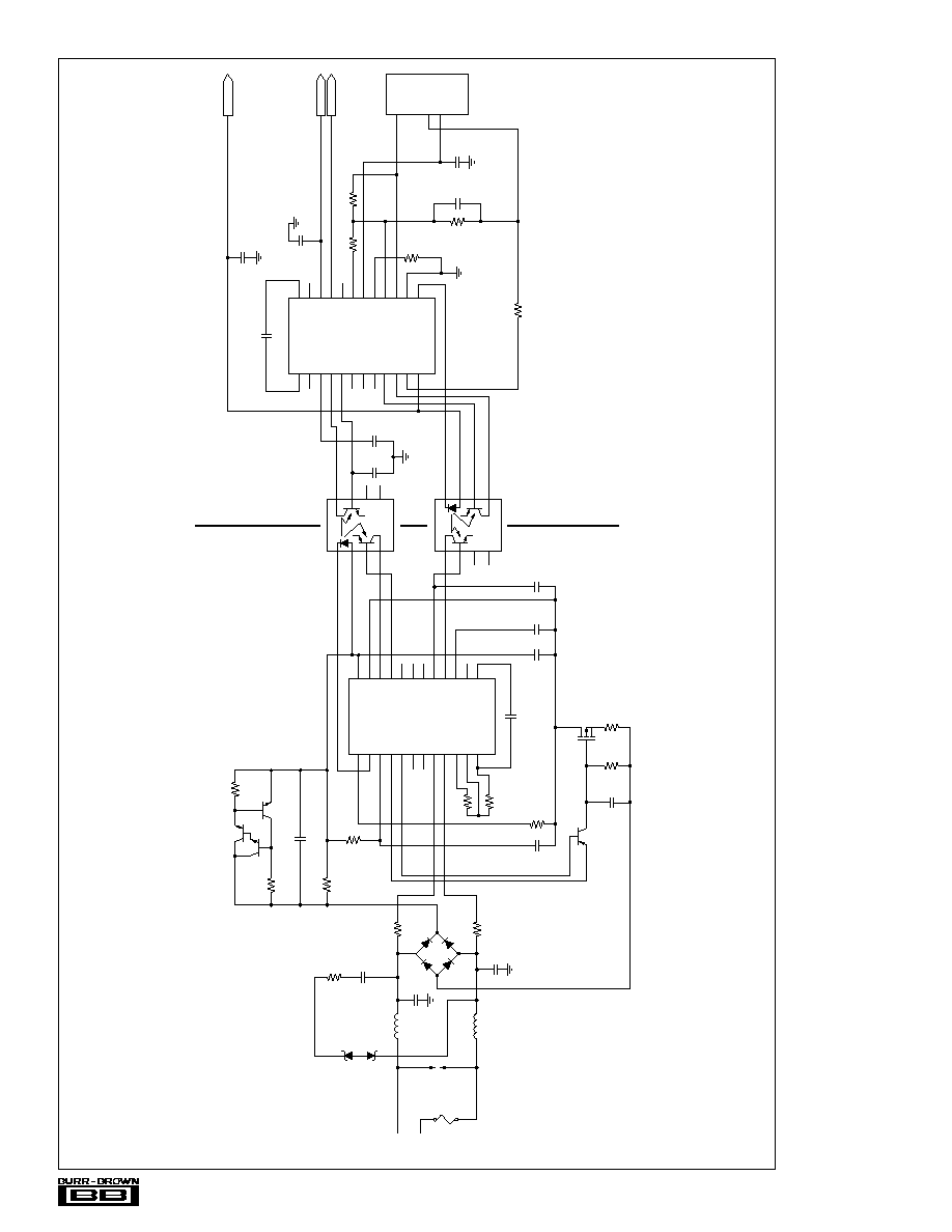
FIGURE 25. Modem AFE Application Circuit.
HLDR
LEDCT
HLDCAP
HKP
HKN
LINPWR
HLFWV
LR1
LR2
END
CEN
C1A
V
DD
V
SS
SRVCT
SRVAN
HIN
VFCAP
ONHKMC
TXAN
TXCT
C2
BIASEN
C1B
1
2
3
4
5
6
7
8
9
10
11
12
24
23
22
21
20
19
18
17
16
15
14
13
U1
DL207
IL388
8
7
6
5
1
2
3
4
R
5
150k
R
6
150k
C
1
15nF
C
1
15nF
C
3
150nF
C
4
27nF
R
2
10M
D2 Bridge
R
1
V
16.5
1%
R
9
3.9
R
4
356k
Q
2
TN2540
SOT89
Q
1
MMBT6520
SOT23
R
3
10M
C
23
V
0.33
µ
F
250V
R
20
V
15k
C
15
1nF
L
2
LI0805D121R
P3100BA70
V
RV
1
L
1
LI0805D121R
D
1
CMPZDA18V
C
14
1nF
C
8
V
15nF
C
2
150nF
C
9
470pF
C
7
68nF
C
10
470pF
IL388
U4
U3
1
2
3
4
8
7
6
5
RING
TIP
F1
F1250T
R
19
V
2.4k
1W, 2010
R
16
V
6.8M
R
18
V
12
Q
3
V
FZT605
Q
4
V
BC817-40
C
22
22
µ
F, 35V
R
14
V
0
+
+
C1B
V
REF
C2
RXCT
RXAN
ONHKML
ONHKM
HIN
SRVAN
SRVCT
TXMP
V
DD
C1A
LSTAT
RNG
OFFHKL
OFFHK
RXOUT
ACREF
TXBIAS
AUDIN
AUDOUT
V
SS
LEDCT
1
2
3
4
5
6
7
8
9
10
11
12
24
23
22
21
20
19
18
17
16
15
14
13
U2
DM207
V
IN
V
OUT
V
COM
4
22
1
U5
PCM3500
R
10
10k
R
7
25.5k
R
13
V
27k
C
17
V
4.7nF
R
14
22k
RINGD
+3.3V to 7V
OH≠
R
8
121k
C
5
15nF
C
18
1
µ
F
C
20
10
µ
F
ISOLATION BARRIER
ISOLATION BARRIER
NOTES: All resistors are 0.1W, 5%, 0805, unless otherwise noted.
All capacitors values are 10%, unless otherwise noted.
V
Optional components.
Æ
25
PCM3500
Software Modem AFE Application Circuit
Figure 25 shows an applications circuit which utilizes the
PCM3500 and the DAA2000 from Infineon Technologies
(Siemens) to implement a complete modem AFE. The
DAA2000 provides modem-side (DM207) and line-side
(DL207) interfaces, with optical isolation separating the
functions. The PCM3500 is connected to the modem-side of
the DAA2000. The PCM3500's serial interface and hard-
ware mode controls are connected to the host CPU.
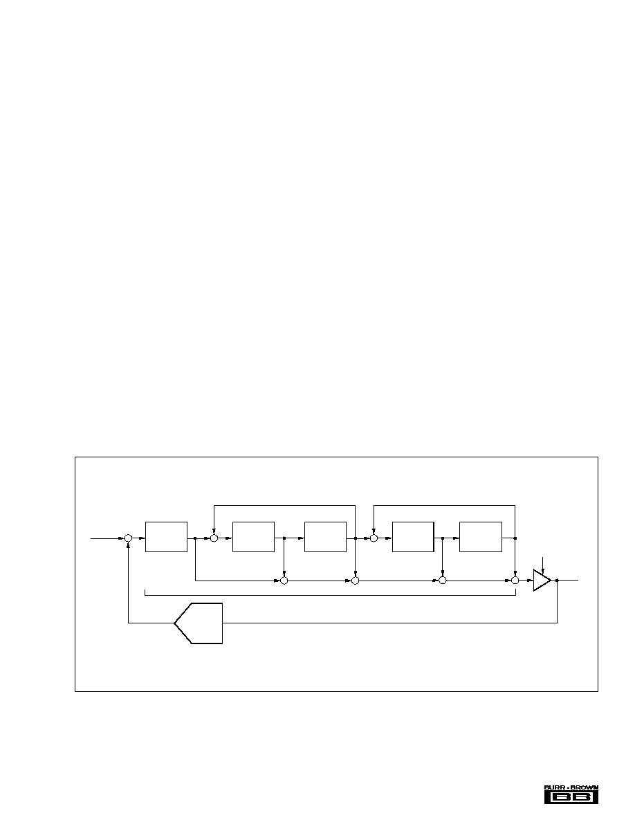
THEORY OF OPERATION
ADC SECTION
The PCM3500 A/D converter consists of two reference
circuits, a mono single-to-differential converter, a fully dif-
ferential 5th-order delta-sigma modulator, a decimation fil-
ter (including digital high pass), and a serial interface circuit.
The block diagram on the front page of this data sheet
illustrates the architecture of the ADC section, Figure 21
shows the single-to-differential converter, and Figure 26
illustrates the architecture of the 5th-order delta-sigma modu-
lator and transfer functions.
An internal reference circuit with three external capacitors
provides all reference voltages which are required by the
ADC, which defines the full-scale range for the converter.
The internal single-to-differential voltage converter saves
the design, space and extra parts needed for external cir-
cuitry required by many delta-sigma converters. The internal
full-differential signal processing architecture provides a
wide dynamic range and excellent power supply rejection
performance. The input signal is sampled at a 64x
oversampling rate, eliminating the need for a sample-and-
hold circuit, and simplifying anti-alias filtering require-
ments. The 5th-order delta-sigma noise shaper consists of
five integrators which use a switched-capacitor topology, a
comparator, and a feedback loop consisting of a one-bit
DAC. The delta-sigma modulator shapes the quantization
noise, shifting it out of the audio band in the frequency
domain. The high order of the modulator enables it to
randomize the modulator outputs, reducing idle tone levels.
The 64f
S
one-bit data stream from the modulator is con-
verted to 1f
S
, 16-bit data words by the decimation filter,
which also acts as a low-pass filter to remove the shaped
quantization noise. The DC components can be removed by
a high-pass filter function contained within the decimation
filter.
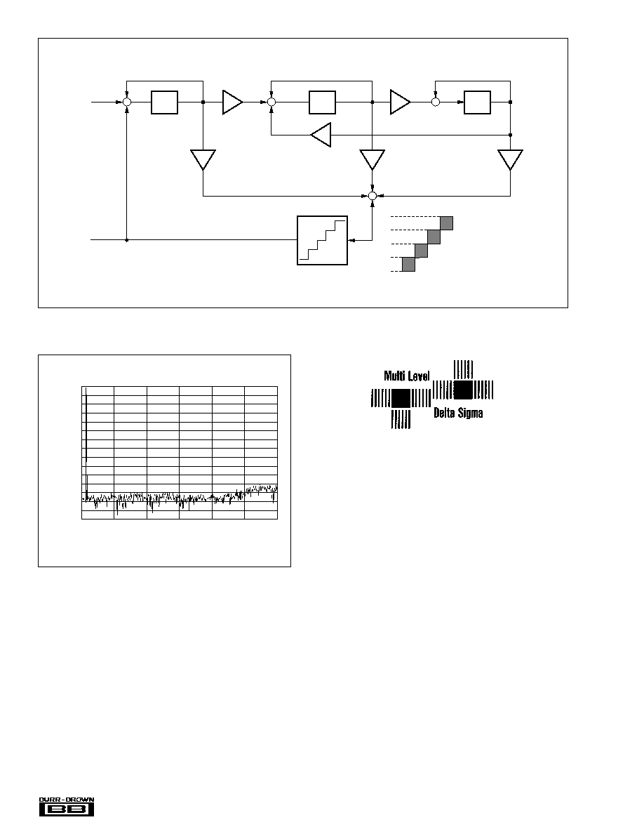
DAC SECTION
The delta-sigma DAC section of PCM3500 is based on a 5-
level amplitude quantizer and a 3rd-order noise shaper. This
section converts the oversampled input data to 5-level delta-
sigma format. A block diagram of the 5-level delta-sigma
modulator is shown in Figure 27. This 5-level delta-sigma
modulator has the advantage of stability and clock jitter
sensitivity over the typical one-bit (2 level) delta-sigma
modulator. The combined oversampling rate of the delta-
sigma modulator and the internal 8x interpolation filter is
64f
S
for a 512f
S
system clock. The theoretical quantization
noise performance of the 5-level delta-sigma modulator is
shown in Figure 28.
+
+
≠
+
+
+
5th SW-CAP
Integrator
4th SW-CAP
Integrator
3rd SW-CAP
Integrator
2nd SW-CAP
Integrator
1st SW-CAP
Integrator
+
+
+
+
≠
+
+
≠
1-Bit
DAC
H(z)
Qn(z)
Analog In
X(z)
Digital Out
Y(z)
Y(z) = STF(z) ∑ X(z) + NTF(z) ∑ Qn(z)
Signal Transfer Function
Noise Transfer Function
STF(z) = H(z) / [1 + H(z)]
NTF(z) = 1/ [1 + H(z)]
Comparator
FIGURE 26. Simplified 5th-Order Delta-Sigma Modulator.
Æ
26
PCM3500
Out
64f
S
In
8f
S
18-Bit
+
+
+
4
3
2
1
0
5-level Quantizer
+
≠
+
Z
≠1
+
≠
+
Z
≠1
+
+
Z
≠1
FIGURE 27. 5-Level Delta-Sigma Modulator Block Digram.
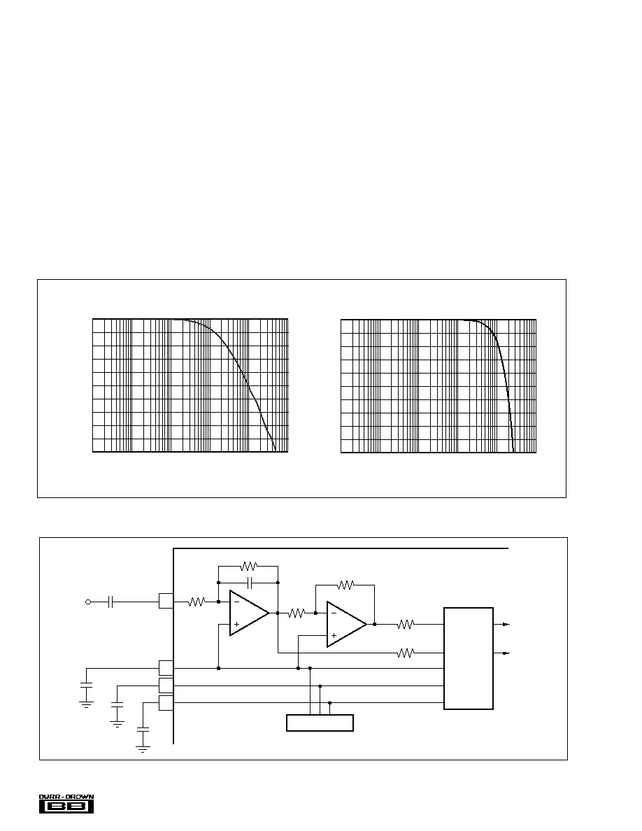
FIGURE 28. Quantization Noise Spectrum.
3rd-ORDER
MODULATOR
Frequency (kHz)
Gain (≠dB)
0
≠10
≠20
≠30
≠40
≠50
≠60
≠70
≠80
≠90
≠100
≠110
≠120
≠130
≠140
≠150
0
5
10
15
20
25
30

PACKAGING INFORMATION
ORDERABLE DEVICE
STATUS(1)
PACKAGE TYPE
PACKAGE DRAWING
PINS
PACKAGE QTY
PCM3500E
ACTIVE
SSOP
DB
24
58
PCM3500E/2K
ACTIVE
SSOP
DB
24
2000
(1) The marketing status values are defined as follows:
ACTIVE: Product device recommended for new designs.
LIFEBUY: TI has announced that the device will be discontinued, and a lifetime-buy period is in effect.
NRND: Not recommended for new designs. Device is in production to support existing customers, but TI does not recommend using this part in
a new design.
PREVIEW: Device has been announced but is not in production. Samples may or may not be available.
OBSOLETE: TI has discontinued the production of the device.
PACKAGE OPTION ADDENDUM
www.ti.com
3-Oct-2003

IMPORTANT NOTICE
Texas Instruments Incorporated and its subsidiaries (TI) reserve the right to make corrections, modifications,
enhancements, improvements, and other changes to its products and services at any time and to discontinue
any product or service without notice. Customers should obtain the latest relevant information before placing
orders and should verify that such information is current and complete. All products are sold subject to TI's terms
and conditions of sale supplied at the time of order acknowledgment.
TI warrants performance of its hardware products to the specifications applicable at the time of sale in
accordance with TI's standard warranty. Testing and other quality control techniques are used to the extent TI
deems necessary to support this warranty. Except where mandated by government requirements, testing of all
parameters of each product is not necessarily performed.
TI assumes no liability for applications assistance or customer product design. Customers are responsible for
their products and applications using TI components. To minimize the risks associated with customer products
and applications, customers should provide adequate design and operating safeguards.
TI does not warrant or represent that any license, either express or implied, is granted under any TI patent right,
copyright, mask work right, or other TI intellectual property right relating to any combination, machine, or process
in which TI products or services are used. Information published by TI regarding third-party products or services
does not constitute a license from TI to use such products or services or a warranty or endorsement thereof.
Use of such information may require a license from a third party under the patents or other intellectual property
of the third party, or a license from TI under the patents or other intellectual property of TI.
Reproduction of information in TI data books or data sheets is permissible only if reproduction is without
alteration and is accompanied by all associated warranties, conditions, limitations, and notices. Reproduction
of this information with alteration is an unfair and deceptive business practice. TI is not responsible or liable for
such altered documentation.
Resale of TI products or services with statements different from or beyond the parameters stated by TI for that
product or service voids all express and any implied warranties for the associated TI product or service and
is an unfair and deceptive business practice. TI is not responsible or liable for any such statements.
Following are URLs where you can obtain information on other Texas Instruments products and application
solutions:
Products
Applications
Amplifiers
amplifier.ti.com
Audio
www.ti.com/audio
Data Converters
dataconverter.ti.com
Automotive
www.ti.com/automotive
DSP
dsp.ti.com
Broadband
www.ti.com/broadband
Interface
interface.ti.com
Digital Control
www.ti.com/digitalcontrol
Logic
logic.ti.com
Military
www.ti.com/military
Power Mgmt
power.ti.com
Optical Networking
www.ti.com/opticalnetwork
Microcontrollers
microcontroller.ti.com
Security
www.ti.com/security
Telephony
www.ti.com/telephony
Video & Imaging
www.ti.com/video
Wireless
www.ti.com/wireless
Mailing Address:
Texas Instruments
Post Office Box 655303 Dallas, Texas 75265
Copyright
2003, Texas Instruments Incorporated