Document Outline
- FEATURES
- APPLICATIONS
- DESCRIPTION
- ORDERING INFORMATION(1)
- ABSOLUTE MAXIMUM RATINGS
- ELECTRICAL CHARACTERISTICS
- PIN ASSIGNMENTS
- Terminal Functions
- TYPICAL CHARACTERISTICS
- PRODUCT OVERVIEW
- ANALOG OUTPUTS
- VOLTAGE REFERENCES
- SAMPLING MODES
- SYSTEM CLOCK REQUIREMENTS
- RESET OPERATION
- POWER-DOWN OPERATION
- AUDIO SERIAL PORT
- STANDALONE MODE CONFIGURATION
- Sampling Mode
- Audio Data Format
- Soft Mute Function
- Digital De-Emphasis
- SOFTWARE MODE CONFIGURATION
- Digital Attenuation
- Digital De-Emphasis
- Soft Mute
- Zero Data Mute
- Output Phase Reversal
- Sampling Mode
- Power-Down Modes
- Software Reset
- Audio Data Formats, LRCK Polarity, and BCK Sampling Edge
- SERIAL PERIPHERAL INTERFACE (SPI) PORT OPERATION
- CONTROL REGISTER DEFINITIONS (SOFTWARE MODE ONLY)
- Register 1: Attenuation Control Register - Channel 1
- Register 2: Attenuation Control Register Ö Channel 2
- Register 3: Attenuation Control Register Ö Channel 3
- Register 4: Attenuation Control Register Ö Channel 4
- Register 5: Function Control Register
- Register 6: System Control Register
- Register 7: Audio Serial Port Control Register for Channels 1 through 4
- Register 1: Attenuation Control Register - Channel 5
- Register 2: Attenuation Control Register Ö Channel 6
- Register 3: Attenuation Control Register Ö Channel 7
- Register 4: Attenuation Control Register Ö Channel 8
- Register 5: Function Control Register
- Register 6: System Control Register
- Register 7: Audio Serial Port Control Register for Channels 5 through 8
- APPLICATIONS INFORMATION
- BASIC CIRCUIT CONFIGURATIONS
- ANALOG OUTPUT FILTER CIRCUITS
FEATURES
D
Eight High-Performance, Multi-Level,
Delta-Sigma Digital-to-Analog Converters
D
Differential Voltage Outputs:
- Full-Scale Output (Differential): 6.15V
PP
D
Supports Sampling Frequencies up to 216kHz
D
Typical Dynamic Performance (24-Bit Data):
- Dynamic Range (A-Weighted): 118dB
- THD+N: -100dB
D
Linear Phase, 8x Oversampling Digital
Interpolation Filter
D
Digital De-Emphasis Filters for 32kHz,
44.1kHz, and 48kHz Sampling Rates
D
Soft Mute Function:
- All-Channel Mute via the MUTE Input Pin
- Per-Channel Mute Available in Software
Mode
D
Digital Attenuation (Software Mode Only):
- Attenuation Range: 0dB to -119.5dB
- 256 Steps with 0.5dB per Step
D
Output Phase Inversion (Software Mode Only)
D
Zero Data Mute (Software Mode Only)
D
Audio Serial Port:
- Supports Left-Justified, Right-Justified,
I
2
S
E
, and TDM Data Formats
- Accepts 16-, 18-, 20, and 24-Bit Two's
Complement PCM Audio Data
D
Standalone or Software-Controlled
Configuration Modes
D
Five-Wire Serial Peripheral Interface (SPI
E
)
Port Provides Control Register Access in
Software Mode
D
Power Supplies: +5V Analog, +3.3V Digital
D
Power Dissipation:
- 406mW typical with f
S
= 48kHz
- 440mW typical with f
S
= 96kHz
- 472mW typical with f
S
= 192kHz
D
Power-Down Modes
D
64-Lead HTQFP Package
APPLICATIONS
D
Digital Mixing Consoles
D
Digital Audio Workstations
D
Digital Audio Effects Processors
D
Broadcast Studio Equipment
D
Surround-Sound Processors
D
High-End A/V Receivers
DESCRIPTION
The PCM4108 is a high-performance, eight-channel
digital-to-analog (D/A) converter designed for use in
professional audio applications. The PCM4108 supports
16- to 24-bit linear PCM input data, with sampling
frequencies up to 216kHz. The PCM4108 features lower
power consumption, making it ideal for use in high channel
count applications by lowering the overall power budget
required for the D/A conversion sub-system.
The PCM4108 features a multi-bit delta-sigma
architecture, followed by a switched capacitor output filter.
This architecture yields lower out-of-band noise and a high
tolerance to system clock phase jitter. Differential voltage
outputs are provided for each channel and are well-suited
to high-performance audio applications. The differential
outputs are easily converted to a single-ended output
using an external op amp IC.
The PCM4108 includes a flexible audio serial port
interface, which supports standard and time division
multiplexed (TDM) formats. In addition, the PCM4108
offers two configuration modes: Standalone and
Software-Controlled. The Standalone mode provides
dedicated control pins for configuring a subset of the
available PCM4108 functions, while Software mode
utilizes a serial peripheral interface (SPI) port for
accessing the complete feature set via internal control
registers.
The PCM4108 operates from a +5V analog power supply
and a +3.3V digital power supply. The digital I/O is
compatible with +3.3V logic families. The PCM4108 is
available in a 64-lead HTQFP package.
PRODUCT PREVIEW
All trademarks are the property of their respective owners.
PCM4108
SBAS354 - JUNE 2005
High Performance, 24 Bit, 216kHz Sampling, Eight Channel Audio
Digital to Analog Converter
PRODUCT PREVIEW information concerns products in the formative or design
phase of development. Characteristic data and other specifications are design
goals. Texas Instruments reserves the right to change or discontinue these
products without notice.
www.ti.com
Copyright
2005, Texas Instruments Incorporated
Please be aware that an important notice concerning availability, standard warranty, and use in critical applications of Texas Instruments
semiconductor products and disclaimers thereto appears at the end of this data sheet.
PCM4108
SBAS354 - JUNE 2005
www.ti.com
2
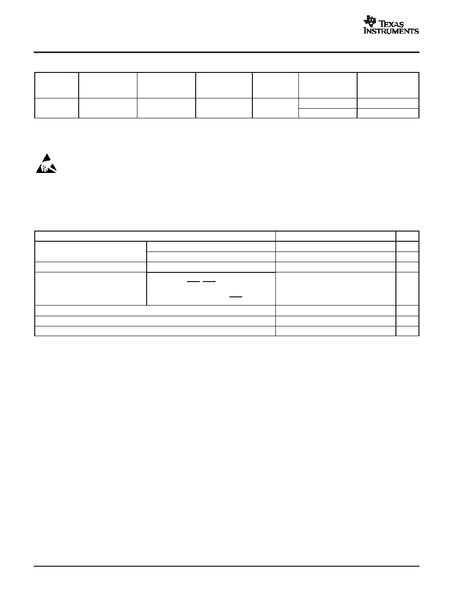
ORDERING INFORMATION
(1)
PRODUCT
PACKAGE-LEAD
PACKAGE
DESIGNATOR
SPECIFIED
TEMPERATURE
RANGE
PACKAGE
MARKING
ORDERING
NUMBER
TRANSPORT
MEDIA, QUANTITY
PCM4108
HTQFP-64
PAP
-10
∞
C to +70
∞
C
PCM4108PAP
PCM4108PAPT
Tape and Reel, 250
PCM4108
HTQFP-64
PAP
-10
∞
C to +70
∞
C
PCM4108PAP
PCM4108PAPR
Tape and Reel, 1500
(1) For the most current package and ordering information, see the Package Option Addendum located at the end of this data sheet, or refer to
our web site at www.ti.com.
This integrated circuit can be damaged by ESD. Texas Instruments recommends that all integrated circuits be handled with appropriate
precautions. Failure to observe proper handling and installation procedures can cause damage.
ESD damage can range from subtle performance degradation to complete device failure. Precision integrated circuits may be more susceptible to
damage because very small parametric changes could cause the device not to meet its published specifications.
ABSOLUTE MAXIMUM RATINGS
over operating free-air temperature range unless otherwise noted(1)
PCM4108
UNIT
Supply voltage
VCC
+6.0
V
Supply voltage
VDD
+3.6
V
Ground voltage difference
Any AGND-to-AGND and AGND-to-DGND
±
0.1
V
Digital input voltage
FS0, FS1, FMT0, FMT1, FMT2, CDOUT,
CDIN, CCLK, CSA, CSB, DATA0, DATA1,
DATA2, DATA3, BCK, LRCK, SCKI, SUBA,
SUBB, DEM0, DEM1, MUTE, RST, MODE
-0.3 to (VDD + 0.3)
V
Input current (any pin except supplies)
±
10
mA
Operating temperature range
-10 to +70
∞
C
Storage temperature range, TSTG
-65 to +150
∞
C
(1) Stresses above those listed under Absolute Maximum Ratings may cause permanent damage to the device. Exposure to absolute maximum
conditions for extended periods may degrade device reliability. These are stress ratings only, and functional operation of the device at these or
any other conditions beyond those specified is not implied.
PRODUCT PREVIEW
PCM4108
SBAS354 - JUNE 2005
www.ti.com
3
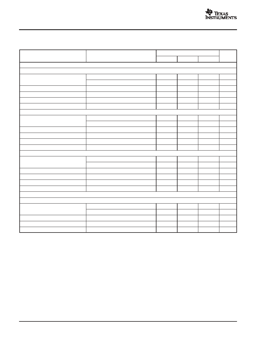
ELECTRICAL CHARACTERISTICS
All parameters are specified at TA = +25
∞
C with VCC = +5V, VDD = +3.3V, and a measurement bandwidth from 10Hz to 20kHz, unless otherwise
noted. System clock frequency is equal to 256fS for Single and Dual Rate sampling modes, and 128fS for Quad Rate sampling mode.
PCM4108
PARAMETER
CONDITIONS
MIN
TYP
MAX
UNITS
RESOLUTION
24
Bits
DATA FORMAT
Audio data formats
Left or Right Justified, I2S, and TDM
Audio data word length
16
24
Bits
Binary data format
Two's Complement Binary, MSB First
CLOCK RATES AND TIMING
Single rate sampling mode
6.144
36.864
MHz
System clock frequency
fSCKI Dual rate sampling mode
13.824
36.864
MHz
System clock frequency
fSCKI
Quad rate sampling mode
13.824
36.864
MHz
Single rate sampling mode
24
54
kHz
Sampling frequency
fS Dual rate sampling mode
54
108
kHz
Sampling frequency
fS
Quad rate sampling mode
108
216
kHz
SPI port data clock
fCCLK
24
MHz
SPI port data clock high time
tCCLKH
15
ns
SPI port data clock low time
tCCLKL
15
ns
DIGITAL INPUT/OUTPUT
Input logic level
VIH
2.0
V
Input logic level
VIL
0.8
V
Input logic current
IIH
VIN = VDD
1
10
µ
A
Input logic current
IIL
VIN = 0V
1
-10
µ
A
Output logic level
VOH
IOH = -2mA
2.4
V
Output logic level
VOL
IOH = +2mA
0.4
V
ANALOG OUTPUTS
Full-scale output voltage, differential
RL = 600
6.15
VPP
Bipolar zero voltage
2.5
V
Output impedance
5
Switched capacitor filter frequency response
f = 20kHz, all sampling modes
-0.2
dB
Gain error
0.5
% FSR
Gain mismatch, channel-to-channel
0.6
% FSR
Bipolar zero error
1
mV
VCOM1 and VCOM2 output voltage
VCC = +5V
2.5
V
VCOM1 and VCOM2 output current
200
µ
A
PRODUCT PREVIEW
PCM4108
SBAS354 - JUNE 2005
www.ti.com
4
ELECTRICAL CHARACTERISTICS (continued)
All parameters are specified at TA = +25
∞
C with VCC = +5V, VDD = +3.3V, and a measurement bandwidth from 10Hz to 20kHz, unless otherwise
noted. System clock frequency is equal to 256fS for Single and Dual Rate sampling modes, and 128fS for Quad Rate sampling mode.
PCM4108
PARAMETER
UNITS
MAX
TYP
MIN
CONDITIONS
DYNAMIC PERFORMANCE WITH 24-BIT DATA(1)
fS = 48kHz
Total harmonic distortion + noise
THD+N
f = 1kHz at 0dBFS
-100
-94
dB
Total harmonic distortion + noise
THD+N
f = 1kHz at -60dBFS
-56
dB
Dynamic range, A-weighted
f = 1kHz at -60dBFS
112
118
dB
Idle channel SNR, A-weighted
All zero input data
119
dB
Idle channel SNR, unweighted
All zero input data
116
dB
Channel separation
f = 1kHz at 0dBFS for active channel
100
110
dB
fS = 96kHz
Total harmonic distortion + noise
THD+N
f = 1kHz at 0dBFS, BW = 10Hz to 40kHz
-100
dB
Total harmonic distortion + noise
THD+N
f = 1kHz at -60dBFS, BW = 10Hz to 40kHz
-53
dB
Dynamic range, A-weighted
f = 1kHz at -60dBFS
118
dB
Idle channel SNR, A-weighted
All zero input data
119
dB
Idle channel SNR, unweighted
All zero input data, BW = 10Hz to 40kHz
113
dB
Channel separation
f = 1kHz at 0dBFS for active channel
110
dB
fS = 192kHz
Total harmonic distortion + noise
THD+N
f = 1kHz at 0dBFS, BW = 10Hz to 40kHz
-97
dB
Total harmonic distortion + noise
THD+N
f = 1kHz at -60dBFS, BW = 10Hz to 40kHz
-53
dB
Dynamic range, A-weighted
f = 1kHz at -60dBFS
118
dB
Idle channel SNR, A-weighted
All zero input data
118
dB
Idle channel SNR, unweighted
All zero input data, BW = 10Hz to 40kHz
113
dB
Channel separation
f = 1kHz at 0dBFS for active channel
110
dB
DYNAMIC PERFORMANCE WITH 16-BIT DATA
fS = 44.1kHz
Total harmonic distortion + noise
THD+N
f = 1kHz at 0dBFS
-92
dB
Total harmonic distortion + noise
THD+N
f = 1kHz at -60dBFS
-33
dB
Dynamic range, A-weighted
f = 1kHz at -60dBFS
96
dB
Idle channel SNR, A-weighted(2)
All zero input data
118
dB
Idle channel SNR, unweighted(2)
All zero input data
115
dB
(1) Dynamic performance parameters are measured using an Audio Precision System Two Cascade or Cascade Plus test system. Input data word
length is 24 bits with triangular PDF dither added for dynamic range and THD+N tests. Idle channel SNR is measured with both the soft and
zero data mute functions disabled and 0% full-scale input data with no dither applied. The measurement bandwidth is limited by using the Audio
Precision 10Hz high-pass filter in combination with either the AES17 20kHz low-pass filter or AES17 40kHz low-pass filter. All A-weighted
measurements are performed using the Audio Precision A-weighting filter in combination with either the 22kHz or 80kHz low-pass filter.
Measurement mode is set to RMS for all parameters. The AVERAGE measurement mode will yield better typical performance numbers.
(2) Idle Channel SNR is not limited by word length.
PRODUCT PREVIEW
PCM4108
SBAS354 - JUNE 2005
www.ti.com
5
ELECTRICAL CHARACTERISTICS (continued)
All parameters are specified at TA = +25
∞
C with VCC = +5V, VDD = +3.3V, and a measurement bandwidth from 10Hz to 20kHz, unless otherwise
noted. System clock frequency is equal to 256fS for Single and Dual Rate sampling modes, and 128fS for Quad Rate sampling mode.
PCM4108
PARAMETER
UNITS
MAX
TYP
MIN
CONDITIONS
DIGITAL FILTERS
Passband
±
0.002dB
0.454fS
Hz
Passband
-3dB
0.487fS
Hz
Stop band
0.546fs
Hz
Passband ripple
±
0.002
dB
Stop band attenuation
0.546fs
-75
dB
Stop band attenuation
0.567fs
-82
dB
Group delay
29/fS
sec
De-emphasis filter error
0.1
dB
POWER SUPPLY
Supply Range
Analog supply, VCC
+4.75
+5.0
+5.25
V
Digital supply, VDD
+3.0
+3.3
+3.6
V
Power-down current
VCC = +5V, VDD = +3.3V
Power-down supply current, ICC + IDD
RST = low, system and audio clocks off
1
mA
Quiescent current
System and audio clocks applied, all 0s data
VCC = +5V, fS =48kHz
64
80
mA
Analog supply, ICC
VCC = +5V, fS =96kHz
64
mA
Analog supply, ICC
VCC = +5V, fS =192kHz
64
mA
VDD = +3.3V, fS =48kHz
26
34
mA
Digital supply, IDD
VDD = +3.3V, fS =96kHz
36
mA
Digital supply, IDD
VDD = +3.3V, fS =192kHz
46
mA
VCC = +5V, VDD = +3.3V
Total power dissipation
fS = 48kHz
406
512
mW
Total power dissipation
fS = 96kHz
440
mW
fS = 192kHz
472
mW
PRODUCT PREVIEW
PCM4108
SBAS354 - JUNE 2005
www.ti.com
6
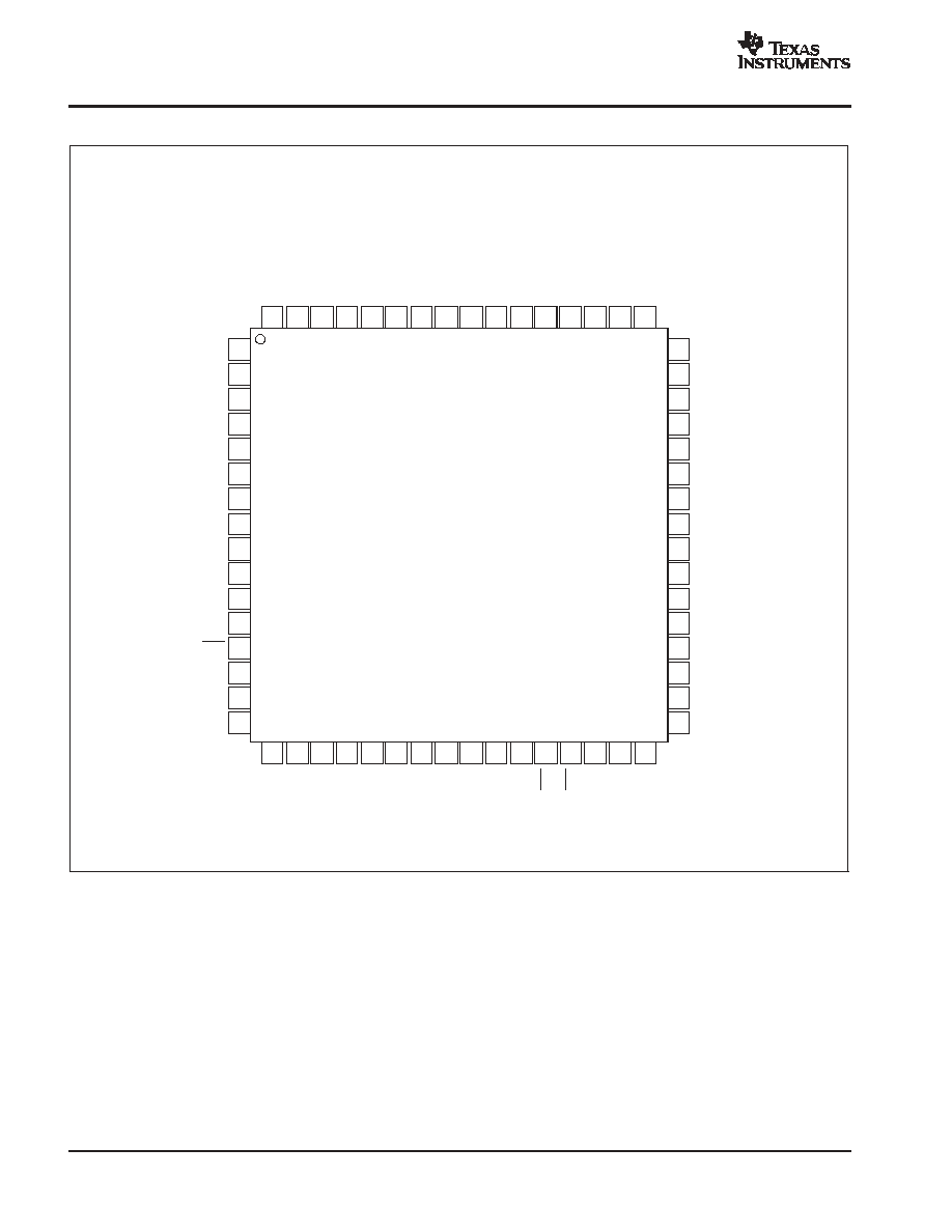
PIN ASSIGNMENTS
HTQFP PACKAGE
(TOP VIEW)
48
47
46
45
44
43
42
41
40
39
38
37
36
35
34
33
V
OUT
4+
V
OUT
4
-
V
OUT
8+
V
OUT
8
-
AGND2
V
REF
2
-
V
REF
2+
NC
NC
NC
NC
FS1
FS0
FMT2
FMT1
FMT0
1
2
3
4
5
6
7
8
9
10
11
12
13
14
15
16
V
OUT
1+
V
OUT
1
-
V
OUT
5+
V
OUT
5
-
AGND1
V
REF
1
-
V
REF
1+
NC
NC
NC
NC
MODE
RST
MUTE
DEM1
DEM0
V
CO
M
1
V
OU
T
2+
V
OU
T
2
-
V
OU
T
6+
V
OU
T
6
-
V
CC
1
V
RE
F
4+
V
OU
T
4
-
V
OU
T
3
-
V
OU
T
3+
V
CC
2
V
RE
F
3
-
V
RE
F
3+
V
OU
T
7
-
V
OU
T
7+
V
CO
M
2
SU
B
A
SU
B
B
SC
K
I
BC
K
LR
C
K
DA
T
A
0
DA
T
A
1
DA
T
A
2
DA
T
A
3
V
DD
DG
ND
CS
A
CS
B
CCL
K
CD
IN
CDO
UT
64
63
62
61
60
59
58
57
56
55
54
17
18
19
20
21
22
23
24
25
26
27
53
52
51
50
49
28
29
30
31
32
PCM4108
PRODUCT PREVIEW
PCM4108
SBAS354 - JUNE 2005
www.ti.com
7
Terminal Functions
TERMINAL
NAME
NO.
I/O
DESCRIPTION
VOUT1+
1
Output
Channel 1 Analog Output, Noninverted
VOUT1-
2
Output
Channel 1 Analog Output, Inverted
VOUT5+
3
Output
Channel 5 Analog Output, Noninverted
VOUT5-
4
Output
Channel 5 Analog Output, Inverted
AGND1
5
Ground
Analog Ground
VREF1-
6
Input
Low Reference Voltage; connect to AGND
VREF1+
7
Input
High Reference Voltage; connect to VCC or external reference
NC
8
-
No Internal Connection
NC
9
-
No Internal Connection
NC
10
-
No Internal Connection
NC
11
-
No Internal Connection
MODE
12
Input
Operating Mode (0 = Standalone, 1 = Software Controlled)
RST
13
Input
Reset/Power Down (Active Low)
MUTE
14
Input
All-Channel Soft Mute (Active High)
DEM1
15
Input
Digital De-Emphasis Filter Configuration
DEM0
16
Input
Digital De-Emphasis Filter Configuration
SUBA
17
Input
Sub-Frame Assignment, Bank A (TDM Formats Only)(1) (Normally connected to DGND)
SUBB
18
Input
Sub-Frame Assignment, Bank B (TDM Formats Only)(1) (Normally connected to VDD)
SCKI
19
Input
System Clock
BCK
20
Input
Audio Bit (or Data) Clock
LRCK
21
Input
Audio Left/Right (or Word) Clock
DATA0
22
Input
Audio Data for Channels 1 and 2 (I2S, Left/Right-Justified formats)
or Audio Data for Channels 1 through 4 for TDM Formats
DATA1
23
Input
Audio Data for Channels 3 and 4 (I2S, Left/Right-Justified formats)
DATA2
24
Input
Audio Data for Channels 5 and 6 (I2S, Left/Right-Justified formats) or Audio Data for Channels 5
through 8 for TDM formats
DATA3
25
Input
Audio Data for Channels 7 and 8 (I2S, Left/Right-Justified formats)
VDD
26
Power
Digital Power Supply, +3.3V
DGND
27
Ground
Digital Ground
CSA
28
Input
Serial Peripheral Interface (SPI) Chip Select for Bank A registers (Active Low)(1)(2)
CSB
29
Input
Serial Peripheral Interface (SPI) Chip Select for Bank B registers (Active Low)(1)(2)
CCLK
30
Input
Serial Peripheral Interface (SPI) Data Clock
CDIN
31
Input
Serial Peripheral Interface (SPI) Data Input
CDOUT
32
Output
Serial Peripheral Interface (SPI) Data Output
(1) Bank A refers to Channels 1 through 4 and the control register bank used to control the functions associated with these channels, while Bank
B refers to Channels 5 through 8 and the control register bank used to control the functions associated with these channels.
(2) For register write operations, both banks may be selected and written to simultaneously. However, for register read operations, only one bank
may be selected. If both banks are selected for a read operation, the state of the CDOUT pin will be indeterminate.
PRODUCT PREVIEW

PCM4108
SBAS354 - JUNE 2005
www.ti.com
8
Terminal Functions
TERMINAL
NAME
DESCRIPTION
I/O
NO.
FMT0
33
Input
Audio Data Format Configuration
FMT1
34
Input
Audio Data Format Configuration
FMT2
35
Input
Audio Data Format Configuration
FS0
36
Input
Sampling Mode Configuration
FS1
37
Input
Sampling Mode Configuration
NC
38
-
No Internal Connection
NC
39
-
No Internal Connection
NC
40
-
No Internal Connection
NC
41
-
No Internal Connection
VREF2+
42
Input
High Reference Voltage; connect to VCC or external reference
VREF2-
43
Input
Low Reference Voltage; connect to AGND
AGND2
44
Ground
Analog Ground
VOUT8-
45
Output
Channel 8 Analog Output, Inverted
VOUT8+
46
Output
Channel 8 Analog Output, Noninverted
VOUT4-
47
Output
Channel 4 Analog Output, Inverted
VOUT4+
48
Output
Channel 4 Analog Output, Noninverted
VCOM2
49
Output
DC Common-Mode Voltage for Channels 3, 4, 7, and 8
VREF7+
50
Output
Channel 7 Analog Output, Noninverted
VREF7-
51
Output
Channel 7 Analog Output, Inverted
VREF3+
52
Output
Channel 3 Analog Output, Noninverted
VREF3-
53
Output
Channel 3 Analog Output, Inverted
VCC2
54
Power
Analog Power-Supply, +5V
VOUT3+
55
Input
High Reference Voltage; Connect to VCC or External Reference
VOUT3-
56
Input
Low Reference Voltage; Connect to AGND
VOUT4-
57
Input
Low Reference Voltage; Connect to AGND
VOUT4+
58
Input
High Reference Voltage; Connect to VCC or External Reference
VCC1
59
Power
Analog Power-Supply, +5V
VOUT6-
60
Output
Channel 6 Analog Output, Inverted
VOUT6+
61
Output
Channel 6 Analog Output, Noninverted
VOUT2-
62
Output
Channel 2 Analog Output, Inverted
VOUT2+
63
Output
Channel 2 Analog Output, Noninverted
VCOM1
64
Output
DC Common-Mode Voltage for Channels 1, 2, 5, and 6
(1) Bank A refers to Channels 1 through 4 and the control register bank used to control the functions associated with these channels, while Bank
B refers to Channels 5 through 8 and the control register bank used to control the functions associated with these channels.
(2) For register write operations, both banks may be selected and written to simultaneously. However, for register read operations, only one bank
may be selected. If both banks are selected for a read operation, the state of the CDOUT pin will be indeterminate.
PRODUCT PREVIEW
PCM4108
SBAS354 - JUNE 2005
www.ti.com
9
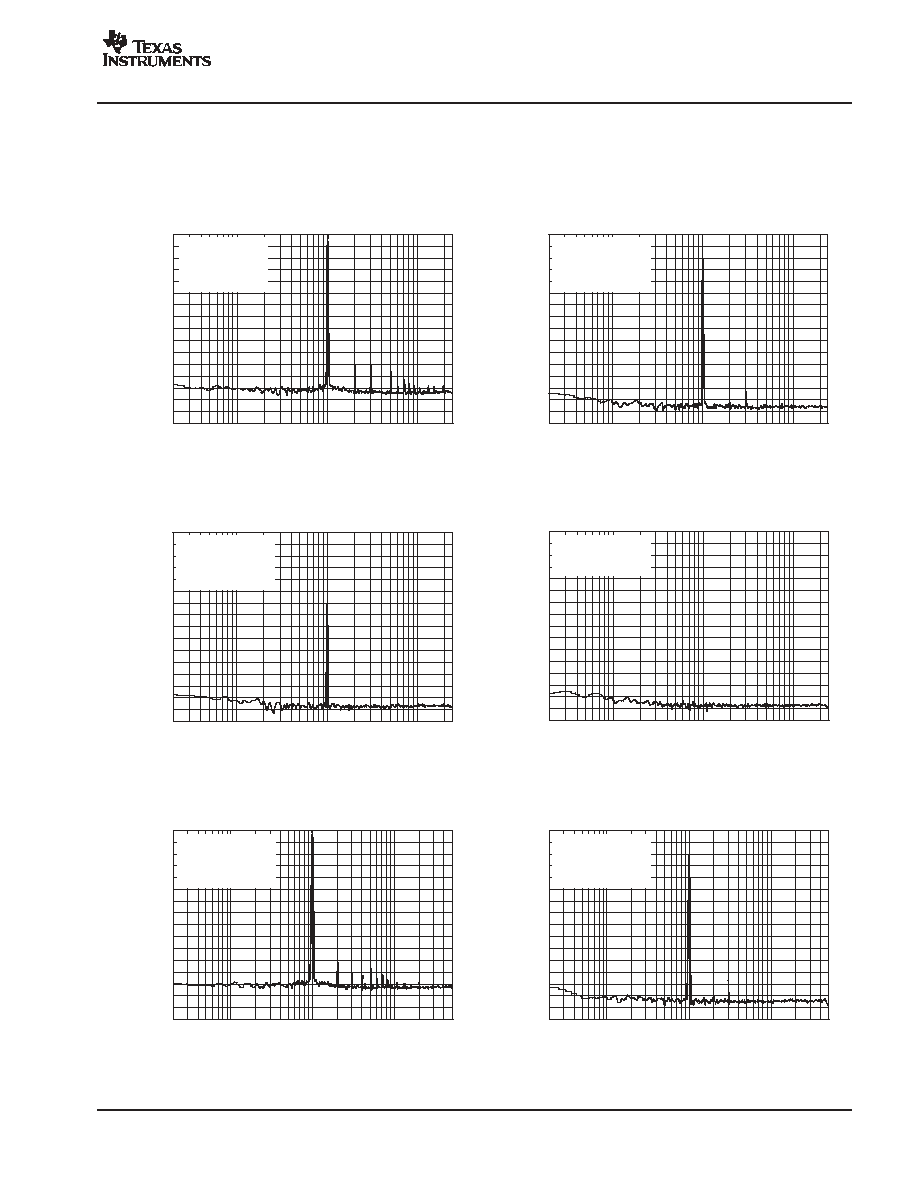
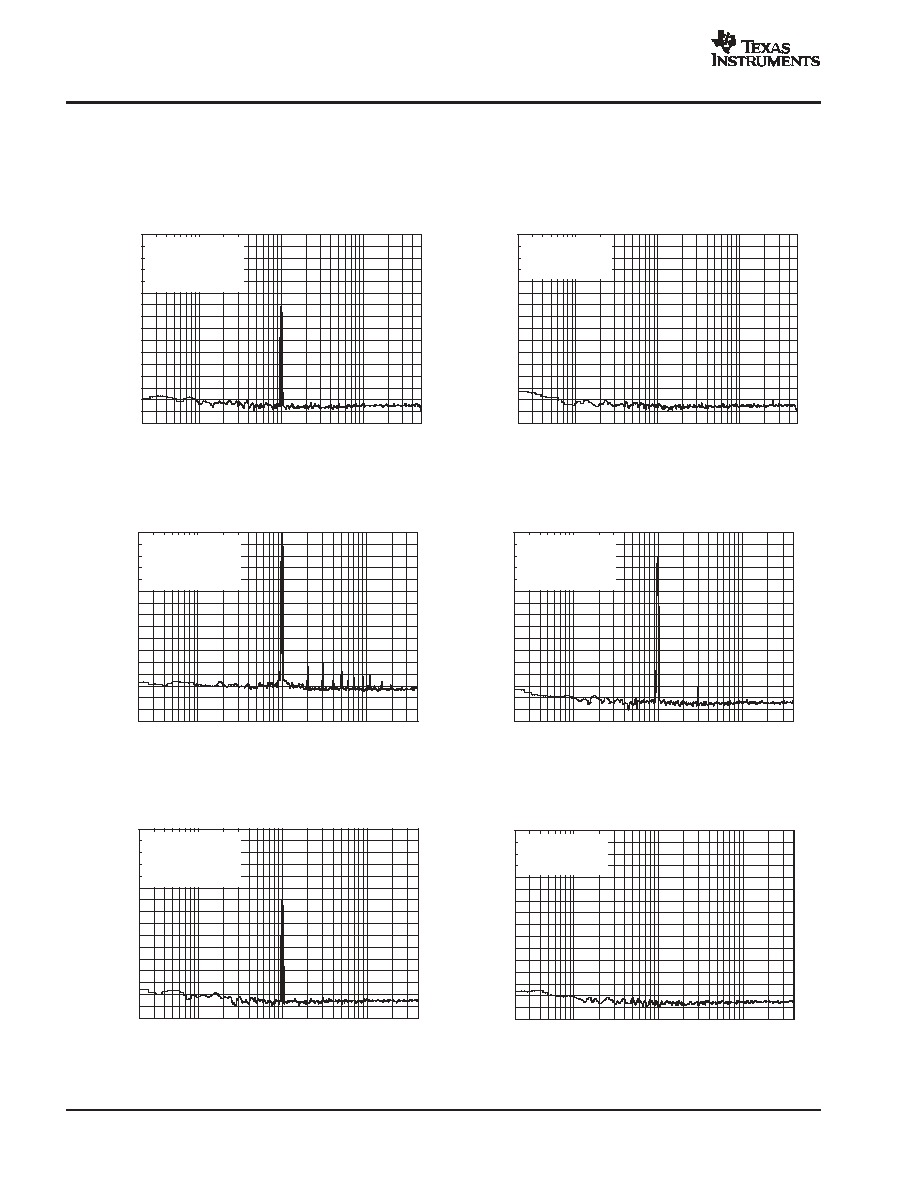
TYPICAL CHARACTERISTICS
All parameters are specified at TA = +25
∞
C with VCC = +5V, VDD = +3.3V, and a measurement bandwidth from 10Hz to 20kHz, unless otherwise
noted. System clock frequency is equal to 256fS for Single and Dual Rate sampling modes, and 128fS for Quad Rate sampling mode.
FFT PLOT
Frequency (Hz)
A
m
p
l
i
t
ude
(
d
B
)
0
-
10
-
20
-
30
-
40
-
50
-
60
-
70
-
80
-
90
-
100
-
110
-
120
-
130
-
140
-
150
-
160
1k
100
20
10k
20k
f
S
= 48kHz
f
IN
= 1kHz
0dBFS Amplitude
24-Bit Data
FFT PLOT
Frequency (Hz)
A
m
p
l
i
t
ude
(
d
B
)
0
-
10
-
20
-
30
-
40
-
50
-
60
-
70
-
80
-
90
-
100
-
110
-
120
-
130
-
140
-
150
-
160
1k
100
20
10k
20k
f
S
= 48kHz
f
IN
= 1kHz
-
20dBFS Amplitude
24-Bit Data
FFT PLOT
Frequency (Hz)
A
m
p
l
i
t
ude
(
d
B
)
0
-
10
-
20
-
30
-
40
-
50
-
60
-
70
-
80
-
90
-
100
-
110
-
120
-
130
-
140
-
150
-
160
1k
100
20
10k
20k
f
S
= 48kHz
f
IN
= 1kHz
-
60dBFS Amplitude
24-Bit Data
FFT PLOT
Frequency (Hz)
A
m
pl
i
t
ude
(
d
B
)
0
-
10
-
20
-
30
-
40
-
50
-
60
-
70
-
80
-
90
-
100
-
110
-
120
-
130
-
140
-
150
-
160
1k
100
20
10k
20k
f
S
= 48kHz
Idle Channel Input
24-Bit Data
FFT PLOT
Frequency (Hz)
A
m
p
l
i
t
ude
(
d
B
)
0
-
10
-
20
-
30
-
40
-
50
-
60
-
70
-
80
-
90
-
100
-
110
-
120
-
130
-
140
-
150
-
160
1k
100
20
10k
40k
f
S
= 96kHz
f
IN
= 1kHz
0dBFS Amplitude
24-Bit Data
FFT PLOT
Frequency (Hz)
A
m
p
l
i
t
ude
(
d
B
)
0
-
10
-
20
-
30
-
40
-
50
-
60
-
70
-
80
-
90
-
100
-
110
-
120
-
130
-
140
-
150
-
160
1k
100
20
10k
40k
f
S
= 96kHz
f
IN
= 1kHz
-
20dBFS Amplitude
24-Bit Data
PRODUCT PREVIEW
PCM4108
SBAS354 - JUNE 2005
www.ti.com
10
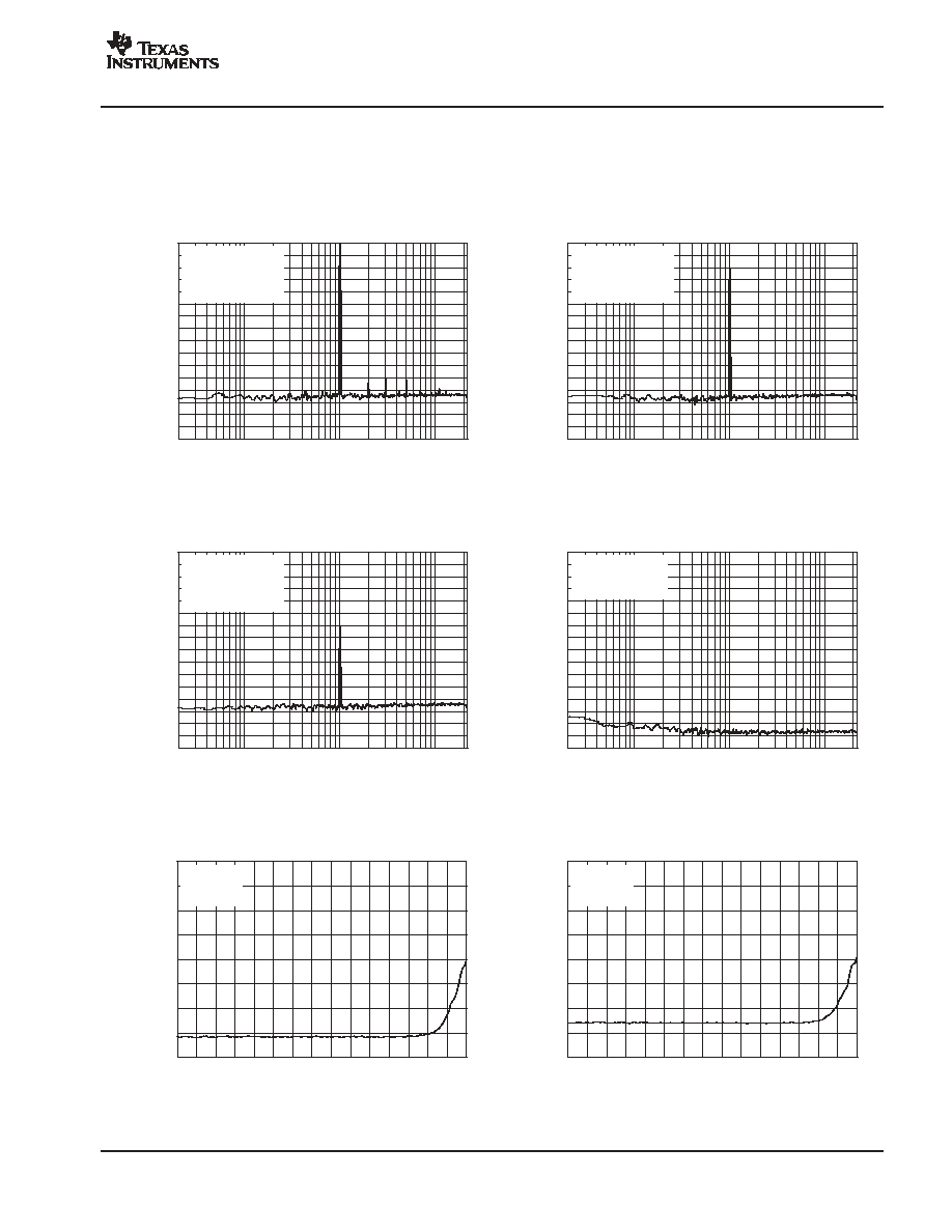
TYPICAL CHARACTERISTICS (continued)
All parameters are specified at TA = +25
∞
C with VCC = +5V, VDD = +3.3V, and a measurement bandwidth from 10Hz to 20kHz, unless otherwise
noted. System clock frequency is equal to 256fS for Single and Dual Rate sampling modes, and 128fS for Quad Rate sampling mode.
FFT PLOT
Frequency (Hz)
A
m
p
l
i
t
ude
(
d
B
)
0
-
10
-
20
-
30
-
40
-
50
-
60
-
70
-
80
-
90
-
100
-
110
-
120
-
130
-
140
-
150
-
160
1k
100
20
10k
40k
f
S
= 96kHz
f
IN
= 1kHz
-
60dBFS Amplitude
24-Bit Data
FFT PLOT
Frequency (Hz)
A
m
p
l
i
t
ude
(
d
B
)
0
-
10
-
20
-
30
-
40
-
50
-
60
-
70
-
80
-
90
-
100
-
110
-
120
-
130
-
140
-
150
-
160
1k
100
20
10k
40k
f
S
= 96kHz
Idle Channel Input
24-Bit Data
FFT PLOT
Frequency (Hz)
A
m
p
l
i
t
ude
(
d
B
)
0
-
10
-
20
-
30
-
40
-
50
-
60
-
70
-
80
-
90
-
100
-
110
-
120
-
130
-
140
-
150
-
160
1k
100
20
10k
40k
f
S
= 192kHz
f
IN
= 1kHz
0dBFS Amplitude
24-Bit Data
FFT PLOT
Frequency (Hz)
A
m
p
l
i
t
ude
(
d
B
)
0
-
10
-
20
-
30
-
40
-
50
-
60
-
70
-
80
-
90
-
100
-
110
-
120
-
130
-
140
-
150
-
160
1k
100
20
10k
40k
f
S
= 192kHz
f
IN
= 1kHz
-
20dBFS Amplitude
24-Bit Data
FFT PLOT
Frequency (Hz)
A
m
p
l
i
t
ude
(
d
B
)
0
-
10
-
20
-
30
-
40
-
50
-
60
-
70
-
80
-
90
-
100
-
110
-
120
-
130
-
140
-
150
-
160
1k
100
20
10k
40k
f
S
= 192kHz
f
IN
= 1kHz
-
60dBFS Amplitude
24-Bit Data
FFT PLOT
Frequency (Hz)
A
m
p
l
i
t
ude
(
d
B
)
0
-
10
-
20
-
30
-
40
-
50
-
60
-
70
-
80
-
90
-
100
-
110
-
120
-
130
-
140
-
150
-
160
1k
100
20
10k
40k
f
S
= 192kHz
Idle Channel Input
24-Bit Data
PRODUCT PREVIEW
PCM4108
SBAS354 - JUNE 2005
www.ti.com
11
TYPICAL CHARACTERISTICS (continued)
All parameters are specified at TA = +25
∞
C with VCC = +5V, VDD = +3.3V, and a measurement bandwidth from 10Hz to 20kHz, unless otherwise
noted. System clock frequency is equal to 256fS for Single and Dual Rate sampling modes, and 128fS for Quad Rate sampling mode.
FFT PLOT
Frequency (Hz)
A
m
p
l
i
t
ude
(
d
B
)
0
-
10
-
20
-
30
-
40
-
50
-
60
-
70
-
80
-
90
-
100
-
110
-
120
-
130
-
140
-
150
-
160
1k
100
20
10k
20k
f
S
= 44.1kHz
f
IN
= 1kHz
0dBFS Amplitude
16-Bit Data
FFT PLOT
Frequency (Hz)
A
m
p
l
i
t
ude
(
d
B
)
0
-
10
-
20
-
30
-
40
-
50
-
60
-
70
-
80
-
90
-
100
-
110
-
120
-
130
-
140
-
150
-
160
1k
100
20
10k
20k
f
S
= 44.1kHz
f
IN
= 1kHz
-
20dBFS Amplitude
16-Bit Data
FFT PLOT
Frequency (Hz)
A
m
p
l
i
t
ude
(
d
B
)
0
-
10
-
20
-
30
-
40
-
50
-
60
-
70
-
80
-
90
-
100
-
110
-
120
-
130
-
140
-
150
-
160
1k
100
20
10k
20k
f
S
= 44.1kHz
f
IN
= 1kHz
-
60dBFS Amplitude
16-Bit Data
FFT PLOT
Frequency (Hz)
A
m
p
l
i
t
ude
(
d
B
)
0
-
10
-
20
-
30
-
40
-
50
-
60
-
70
-
80
-
90
-
100
-
110
-
120
-
130
-
140
-
150
-
160
1k
100
20
10k
20k
f
S
= 44.1kHz
Idle Channel Input
16-Bit Data
THD+N vs AMPLITUDE
Amplitude (dBFS)
T
HD+N
(
d
B
)
-
80
-
85
-
90
-
95
-
100
-
105
-
110
-
115
-
120
-
150
-
140
-
130
-
120
-
110
-
100
-
90
-
80
-
70
-
60
-
50
-
40
-
30
-
20
-
10
0
f
S
= 48kHz
f
IN
= 1kHz
24-Bit Data
THD+N vs AMPLITUDE
Amplitude (dBFS)
TH
D
+
N
(
d
B
)
-
80
-
85
-
90
-
95
-
100
-
105
-
110
-
115
-
120
-
150
-
140
-
130
-
120
-
110
-
100
-
90
-
80
-
70
-
60
-
50
-
40
-
30
-
20
-
10
0
f
S
= 96kHz
f
IN
= 1kHz
24-Bit Data
PRODUCT PREVIEW
PCM4108
SBAS354 - JUNE 2005
www.ti.com
12
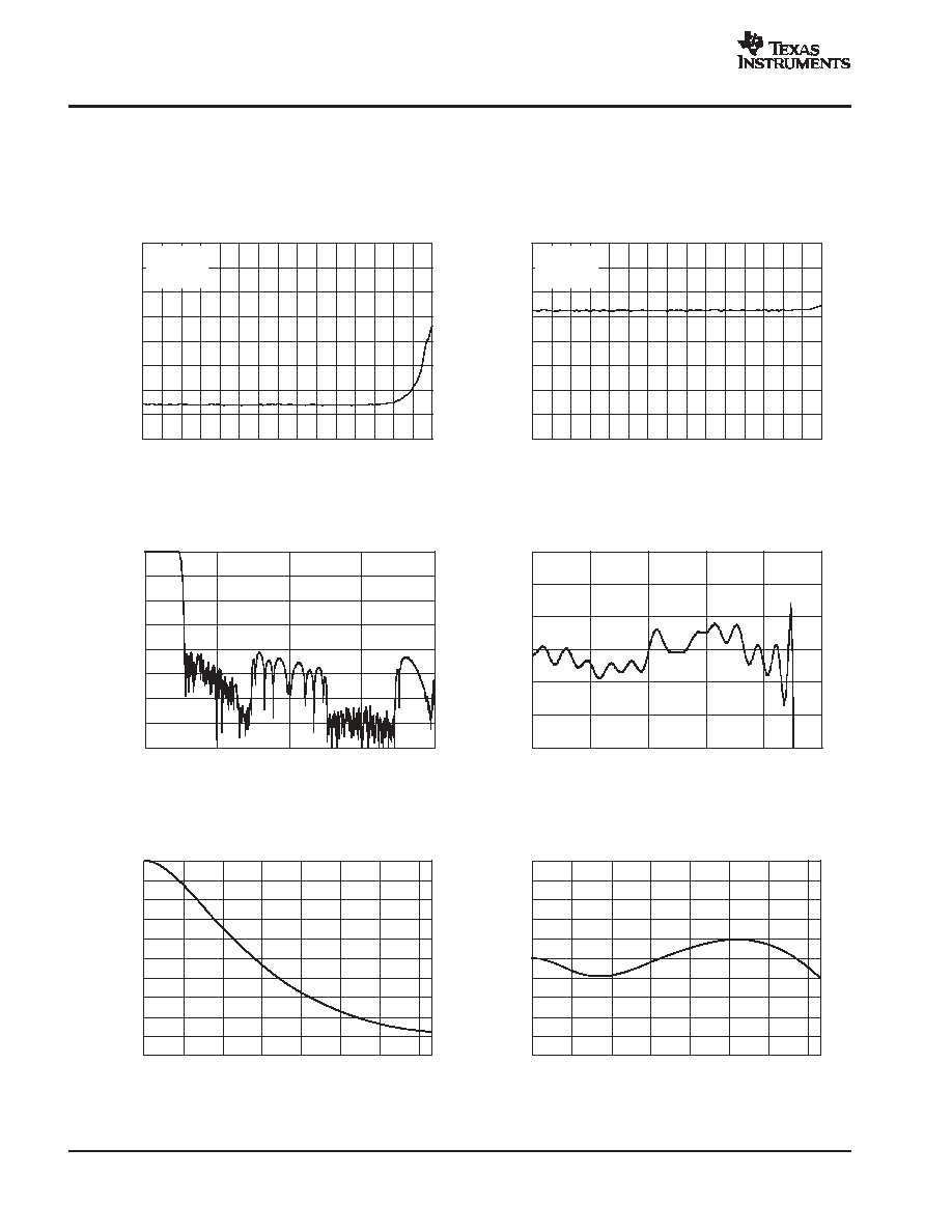
TYPICAL CHARACTERISTICS (continued)
All parameters are specified at TA = +25
∞
C with VCC = +5V, VDD = +3.3V, and a measurement bandwidth from 10Hz to 20kHz, unless otherwise
noted. System clock frequency is equal to 256fS for Single and Dual Rate sampling modes, and 128fS for Quad Rate sampling mode.
THD+N vs AMPLITUDE
Amplitude (dBFS)
TH
D
+
N
(
d
B
)
-
80
-
85
-
90
-
95
-
100
-
105
-
110
-
115
-
120
-
150
-
140
-
130
-
120
-
110
-
100
-
90
-
80
-
70
-
60
-
50
-
40
-
30
-
20
-
10
0
f
S
= 192kHz
f
IN
= 1kHz
24-Bit Data
THD+N vs AMPLITUDE
Amplitude (dBFS)
TH
D
+
N
(
d
B
)
-
80
-
85
-
90
-
95
-
100
-
105
-
110
-
115
-
120
-
150
-
140
-
130
-
120
-
110
-
100
-
90
-
80
-
70
-
60
-
50
-
40
-
30
-
20
-
10
0
f
S
= 44.1kHz
f
IN
= 1kHz
16-Bit Data
0
-
20
-
40
-
60
-
80
-
100
-
120
-
140
-
160
FREQUENCY RESPONSE
0
1
2
3
4
Frequency (x f
S
)
A
m
pl
i
t
ude
(
d
B
)
0.003
0.002
0.001
0
-
0.001
-
0.002
-
0.003
PASSBAND RIPPLE
0
0.1
0.2
0.3
0.4
0.5
Frequency (x f
S
)
A
m
pl
i
t
ude
(
d
B
)
0.0
-
1.0
-
2.0
-
3.0
-
4.0
-
5.0
-
6.0
-
7.0
-
8.0
-
9.0
-
10.0
DE-EMPHASIS FILTER RESPONSE (f
S
= 32kHz)
0
2
4
6
8
10
12
14
Frequency (kHz)
Lev
el
(
d
B
)
0.5
0.4
0.3
0.2
0.1
0.0
-
0.1
-
0.2
-
0.3
-
0.4
-
0.5
DE-EMPHASIS ERROR (f
S
= 32kHz)
0
2
4
6
8
10
12
14
Frequency (kHz)
Er
r
o
r
(
d
B
)
PRODUCT PREVIEW
PCM4108
SBAS354 - JUNE 2005
www.ti.com
13
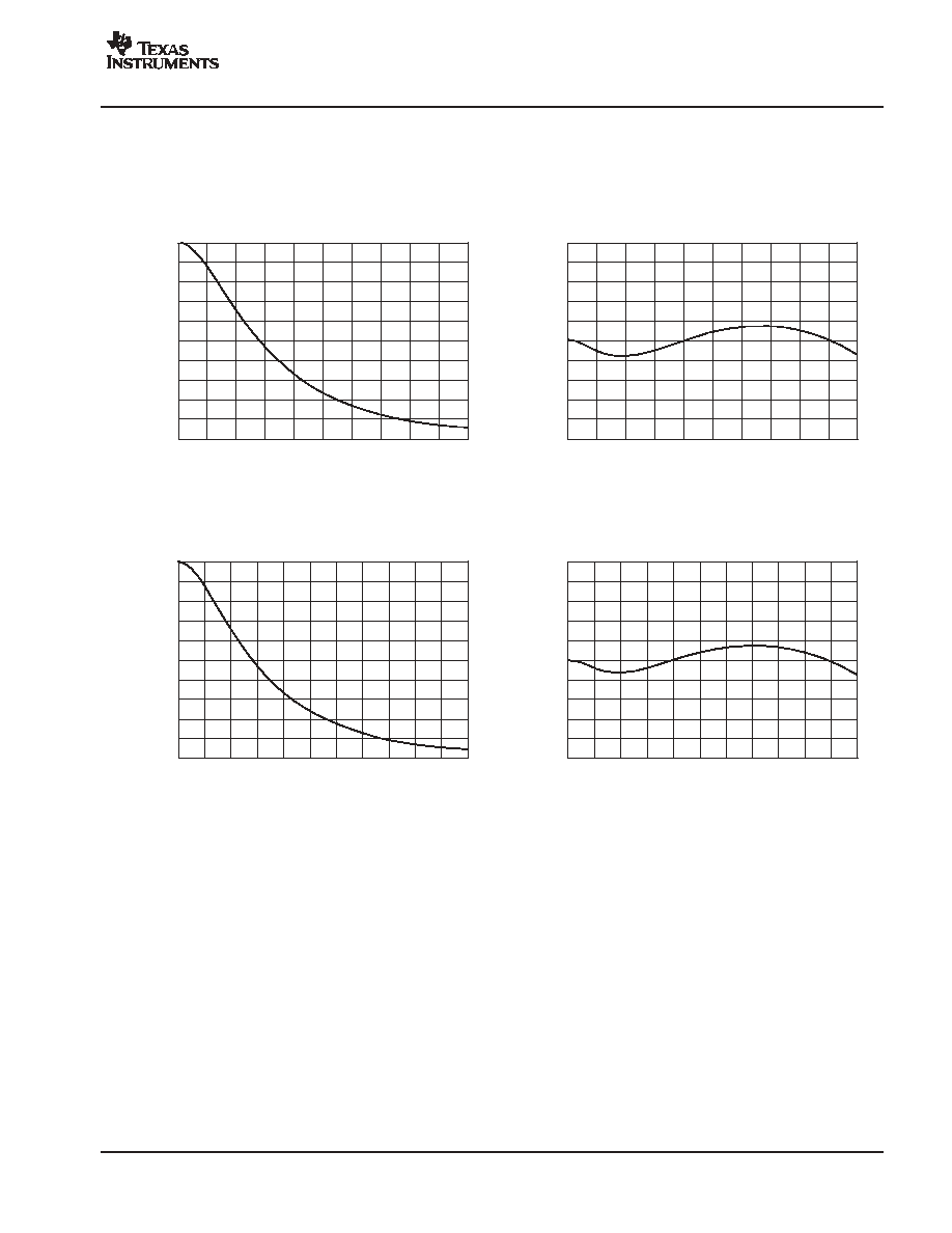
TYPICAL CHARACTERISTICS (continued)
All parameters are specified at TA = +25
∞
C with VCC = +5V, VDD = +3.3V, and a measurement bandwidth from 10Hz to 20kHz, unless otherwise
noted. System clock frequency is equal to 256fS for Single and Dual Rate sampling modes, and 128fS for Quad Rate sampling mode.
0.0
-
1.0
-
2.0
-
3.0
-
4.0
-
5.0
-
6.0
-
7.0
-
8.0
-
9.0
-
10.0
DE-EMPHASIS FILTER RESPONSE (f
S
= 44.1kHz)
0
2
4
6
8
10
12
14
16
18
20
Frequency (kHz)
Lev
el
(
d
B
)
0.5
0.4
0.3
0.2
0.1
0.0
-
0.1
-
0.2
-
0.3
-
0.4
-
0.5
DE-EMPHASIS ERROR (f
S
= 44.1kHz)
0
2
4
6
8
10
12
14
16
18
20
Frequency (kHz)
Er
r
o
r
(
d
B
)
0.0
-
1.0
-
2.0
-
3.0
-
4.0
-
5.0
-
6.0
-
7.0
-
8.0
-
9.0
-
10.0
DE- EMPHASIS FILTER RESPONSE (f
S
= 48kHz)
0
2
4
6
8
10
12
14
16
18
22
Frequency (kHz)
Lev
el
(
d
B
)
0.5
0.4
0.3
0.2
0.1
0.0
-
0.1
-
0.2
-
0.3
-
0.4
-
0.5
DE- EMPHASIS ERROR (f
S
= 48kHz)
0
2
4
6
8
10
12
14
16
18
22
Frequency (kHz)
Er
r
o
r
(
d
B
)
PRODUCT PREVIEW
PCM4108
SBAS354 - JUNE 2005
www.ti.com
14
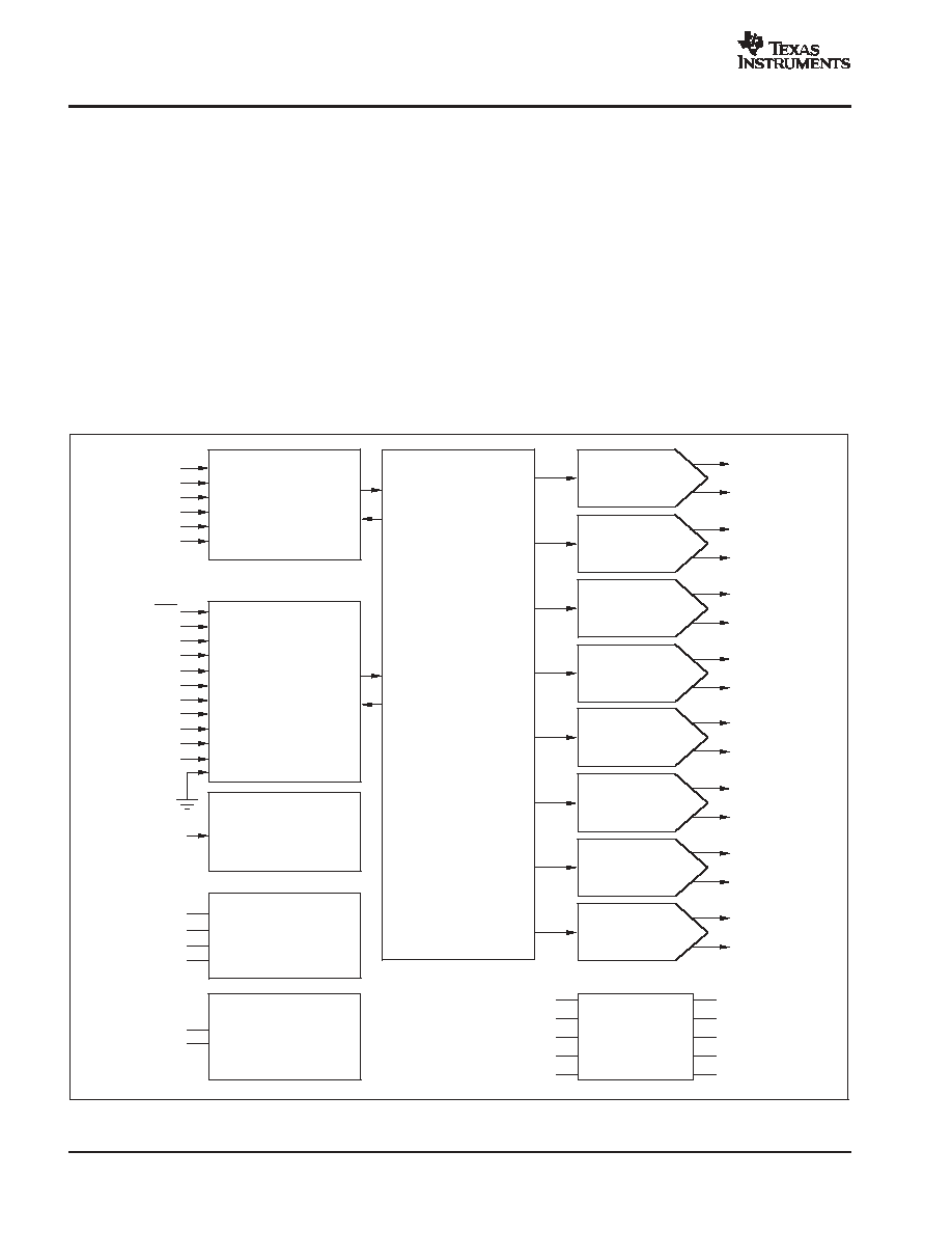
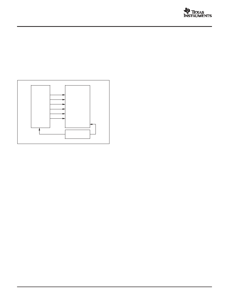
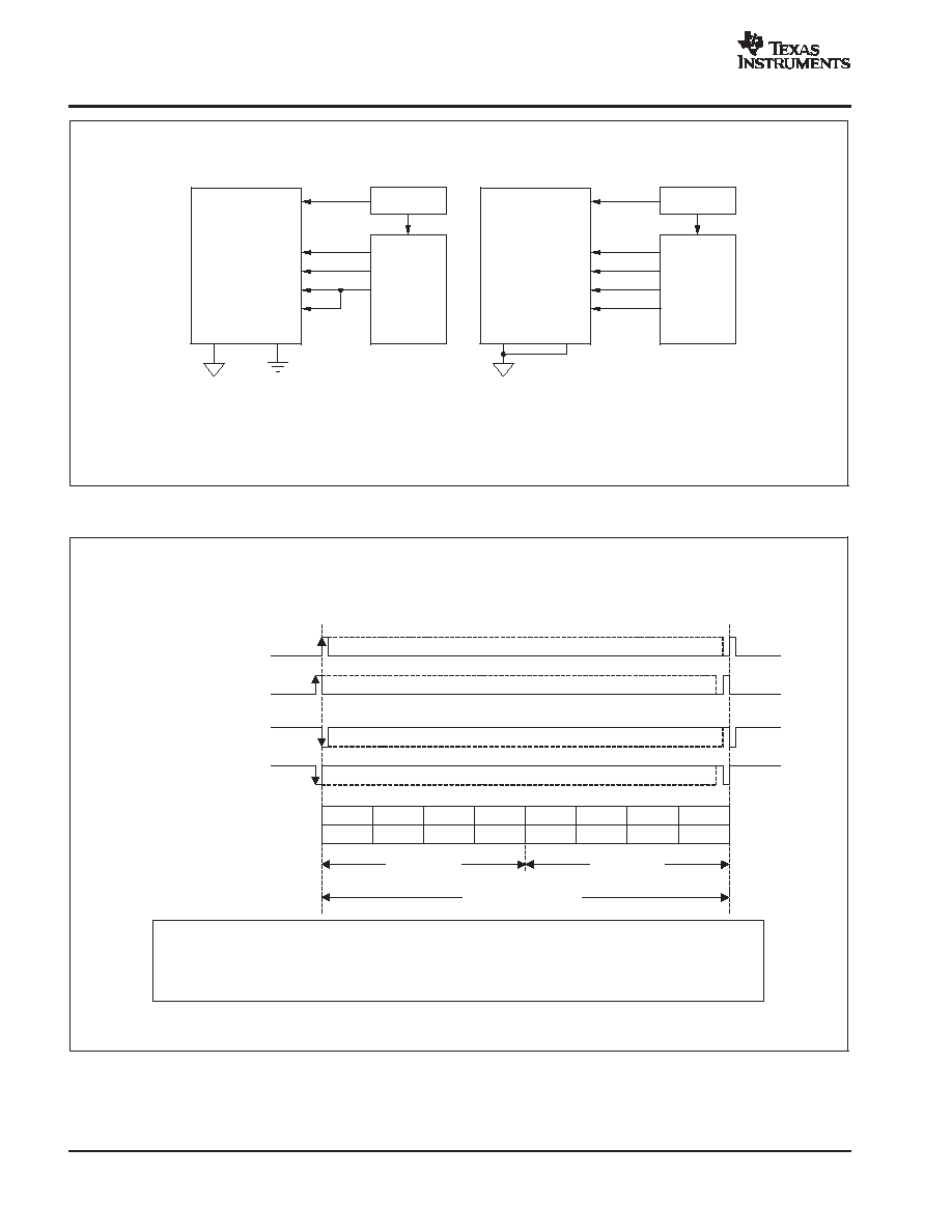
PRODUCT OVERVIEW
The PCM4108 is a high-performance, eight-channel D/A
converter designed for professional audio systems. The
PCM4108 supports 16- to 24-bit linear PCM input data and
sampling frequencies up to 216kHz. The PCM4108
utilizes an 8x oversampling digital interpolation filter,
followed by a multi-level delta-sigma modulator with a
single pole switched capacitor output filter. This
architecture provides excellent dynamic and sonic
performance, as well as high tolerance to clock phase
jitter. Functional block diagrams in Figure 1 and Figure 2
illustrate Standalone and Software modes, respectively.
The PCM4108 incorporates a flexible audio serial port,
which accepts 16- to 24-bit PCM audio data in both
standard audio formats (Left-Justified, Right-Justified, and
Philips I
2
S) and TDM data formats. The TDM formats are
especially useful for interfacing to the synchronous serial
ports of digital signal processors.
The PCM4108 offers two modes for configuration control:
Software and Standalone. Software mode makes use of a
five-wire SPI port to access internal control registers,
allowing configuration of the full PCM4108 feature set.
Standalone mode offers a more limited subset of the
functions available in Software mode, while allowing for a
simplified pin-programmed configuration mode.
Digital
Filtering
and
Functions
Audio
Serial
Port
Control
V
OUT
1+
V
OUT
1
-
V
OUT
2+
V
OUT
2
-
V
OUT
3+
V
OUT
3
-
V
OUT
4+
V
OUT
4
-
Digital
Power
Analog
Power
System Clock
and
Timing
V
CC
1
AGND1
V
CC2
1
AGND2
V
DD
DGND
References
V
REF
1+
V
REF
1
-
V
REF
2+
V
REF
2
-
V
COM
1
V
REF
3+
V
REF
3
-
V
REF
4+
V
REF
4
-
V
COM
2
D/A Converter
and
Output Filter
D/A Converter
and
Output Filter
D/A Converter
and
Output Filter
D/A Converter
and
Output Filter
V
OUT
5+
V
OUT
5
-
V
OUT
6+
V
OUT
6
-
V
OUT
7+
V
OUT
7
-
V
OUT
8+
V
OUT
8
-
D/A Converter
and
Output Filter
D/A Converter
and
Output Filter
D/A Converter
and
Output Filter
D/A Converter
and
Output Filter
LRCK
BCK
DATA0
DATA1
DATA2
DATA3
SCKI
RST
MUTE
DEM0
DEM1
SUBA
SUBB
FMT0
FMT1
FMT2
FS0
FS1
MODE
Figure 1. Functional Block Diagram for Standalone Mode
PRODUCT PREVIEW

PCM4108
SBAS354 - JUNE 2005
www.ti.com
15
Digital
Filtering
and
Functions
Audio
Serial
Port
SPI Port
and
Control
V
OUT
1+
V
OUT
1
-
V
OUT
2+
V
OUT
2
-
V
OUT
3+
V
OUT
3
-
V
OUT
4+
V
OUT
4
-
Digital
Power
Analog
Power
System Clock
and
Timing
V
CC
1
AGND1
V
CC
2
AGND2
V
DD
V
DD
DGND
References
V
REF
1+
V
REF
1
-
V
REF
2+
V
REF
2
-
V
COM
1
V
REF
3+
V
REF
3
-
V
REF
4+
V
REF
4
-
V
COM
2
D/A Converter
and
Output Filter
D/A Converter
and
Output Filter
D/A Converter
and
Output Filter
D/A Converter
and
Output Filter
V
OUT
5+
V
OUT
5
-
V
OUT
6+
V
OUT
6
-
V
OUT
7+
V
OUT
7
-
V
OUT
8+
V
OUT
8
-
D/A Converter
and
Output Filter
D/A Converter
and
Output Filter
D/A Converter
and
Output Filter
D/A Converter
and
Output Filter
LRCK
BCK
DATA0
DATA1
DATA2
DATA3
SCKI
RST
MUTE
SUBA
SUBB
CSA
CSB
CCLK
CDIN
CDOUT
MODE
Figure 2. PCM4108 Functional Block Diagram for Software Mode
ANALOG OUTPUTS
The PCM4108 provides eight differential voltage outputs,
corresponding to audio channels 1 through 8. Refer to the
Terminal Functions table for a pin listing.
Each differential output is typically capable of providing
6.15V full-scale (differential) into a 600
output load. The
output pins are internally biased to the common-mode (or
bipolar zero) voltage, which is nominally V
CC
/2. The output
section of each D/A converter channel includes a
single-pole, switched capacitor low-pass filter circuit. The
switched capacitor filter response tracks with the sampling
frequency of the D/A converter and provides attenuation of
the out-of-band noise produced by the delta-sigma
modulator. An external two-pole continuous time filter is
recommended to further reduce the out-of-band noise
energy and to band limit the output spectrum to
frequencies suitable for audio reproduction. Refer to the
Applications Information section of this data sheet for
recommended output filter circuits.
VOLTAGE REFERENCES
The PCM4108 includes high and low reference pins for the
output channels. V
REF
1+ (pin 7) and V
REF
1- (pin 6)
correspond to Channels 1 and 5. V
REF
2+ (pin 42) and
V
REF
2- (pin 43) correspond to Channels 2 and 6. V
REF
3+
(pin 55) and V
REF
3- (pin 56) correspond to Channels 3
and 7. V
REF
4+ (pin 58) and V
REF
4- (pin 57) correspond to
Channels 4 and 8.
The high reference (+) pin may be connected to the
corresponding V
CC
supply or an external +5.0V reference,
while the low reference (-) pin is connected to analog
PRODUCT PREVIEW

PCM4108
SBAS354 - JUNE 2005
www.ti.com
16
ground. A 0.01
µ
F bypass capacitor should be placed
between the corresponding high and low reference pins.
An X7R ceramic chip capacitor is recommended for this
purpose. In some cases, a larger capacitor may need to be
placed in parallel with the 0.01
µ
F capacitor, with the value
of the larger capacitor being dependent upon the
low-frequency power-supply noise present in the system.
Typical values may range from 1
µ
F to 10
µ
F. Low ESR
tantalum or multilayer ceramic chip capacitors are
recommended. Figure 3 illustrates the recommended
connections for the reference pins.
(1) Capacitor(s) required for each of the four reference pairs.
V
REF
+
(1)
V
COM
1
0.01
µ
F
0.1
µ
F
0.1
µ
F
0.1
µ
F to 10
µ
F
V
CC
V
COM
2
V
REF
-
(1)
Figure 3. Recommended Connections for Voltage
Reference and Common-Mode Output Pins
In addition to the reference pins, there are two
common-mode voltage output pins, V
COM
1 (pin 64) and
V
COM
2 (pin 49). These pins are nominally set to a value
equal to V
CC
/2 by internal voltage dividers. The V
COM
1 pin
is common to both Channels 1, 2, 5, and 6, while the
V
COM
2 pin is common to Channels 3, 4, 7, and 8. A 0.1
µ
F
X7R ceramic chip capacitor should be connected between
the common-mode output pin and analog ground. The
common-mode outputs are used primarily to bias external
output circuitry.
SAMPLING MODES
The PCM4108 can operate in one of three sampling
modes: Single Rate, Dual Rate, or Quad Rate. Sampling
modes are selected by using the FS[1:0] bits in Control
Register 6
in Software mode, or by using the FS0 (pin 36)
and FS1 (pin 37) inputs in Standalone mode.
The Single Rate mode allows sampling frequencies up to
and including 54kHz. The D/A converter performs 128x
oversampling of the input data in Single Rate mode.
The Dual Rate mode allows sampling frequencies greater
than 54kHz, up to and including 108kHz. The D/A
converter performs 64x oversampling of the input data in
Dual Rate mode.
The Quad Rate mode allows sampling frequencies greater
than 108kHz, up to and including 216kHz. The D/A
converter performs 32x oversampling of the input data in
Quad Rate mode.
Refer to Table
1 for examples of system clock
requirements for common sampling frequencies.
SYSTEM CLOCK REQUIREMENTS
The PCM4108 requires a system clock, applied at the
SCKI input (pin 19). The system clock operates at an
integer multiple of the input sampling frequency, or f
S
. The
multiples supported include 128f
S
, 192f
S
, 256f
S
, 384f
S
,
512f
S
, or 768f
S
. The system clock frequency is dependent
upon the sampling mode. Table 1 shows the required
system clock frequencies for common audio sampling
frequencies. Figure 4 shows the system clock timing
requirements.
Although the architecture of the PCM4108 is tolerant to
phase jitter on the system clock, it is recommended that
the user provide a low jitter clock (100ps or less) for optimal
performance.
Table 1. Sampling Modes and System Clock Frequencies for Common Audio Sampling Rates
SAMPLING FREQUENCY, fS
SYSTEM CLOCK FREQUENCY (MHz)
SAMPLING MODE
SAMPLING FREQUENCY, fS
(kHz)
128fS
192fS
256fS
384fS
512fS
768fS
Single Rate
32
n/a
n/a
8.192
12.288
16.384
24.576
Single Rate
44.1
n/a
n/a
11.2896
16.9344
22.5792
33.8688
Single Rate
48
n/a
n/a
12.288
18.432
24.576
36.864
Dual Rate
88.2
n/a
n/a
22.5792
33.8688
n/a
n/a
Dual Rate
96
n/a
n/a
24.576
36.864
n/a
n/a
Quad Rate
176.4
22.5792
33.8688
n/a
n/a
n/a
n/a
Quad Rate
192
24.576
36.864
n/a
n/a
n/a
n/a
PRODUCT PREVIEW

PCM4108
SBAS354 - JUNE 2005
www.ti.com
17
SCKI
t
SCKI
t
SCKIH
t
SCKIL
PARAMETER
DESCRIPTION
MIN
MAX
UNITS
System Clock Period
26
ns
t
SCKIH
System Clock High Pulse Time
12
ns
t
SCKIL
System Clock Low Pulse Time
12
ns
t
SCKI
Figure 4. System Clock Timing Requirements
RESET OPERATION
The PCM4108 includes three reset functions: power-on,
external, and software-controlled. This section describes
each of the three reset functions.
On power up, the internal reset signal is forced low, forcing
the PCM4108 into a reset state. The power-on reset circuit
monitors the V
DD
, V
CC
1, and V
CC
2 power supplies. When
V
DD
exceeds +2.0V (margin of error is
±
400mV) and V
CC
1
and V
CC
2 exceed +4.0V (margin of error is
±
400mV), the
internal reset signal is forced high. The PCM4108 then
waits for the system clock input (SCKI) to become active.
Once the system clock has been detected, the initialization
sequence begins. The initialization sequence requires
1024 system clock periods for completion. When the
initialization sequence is completed, the PCM4108 is
ready to accept audio data at the audio serial port. Figure 5
shows the power-on reset sequence timing.
If the PCM4108 is configured for Software mode control
via the SPI port, all control registers will be reset to their
default state during the initialization sequence. In both
Standalone and Software modes, the analog outputs for all
eight channels are muted during the reset and initialization
sequence. While in mute state, the analog output pins are
driven to the bipolar zero voltage, or V
CC
/2.
The user may force a reset initialization sequence at any
time while the system clock input is active by utilizing the
RST input (pin 13). The RST input is active low, and
requires a minimum low pulse width of 40ns. The
low-to-high transition of the applied reset signal will force
an initialization sequence to begin. As in the case of the
power-on reset, the initialization sequence requires 1024
system clock periods for completion. Figure 6 illustrates
the reset sequence initiated when using the RST input.
A reset initialization sequence is available in Software
mode, using the RST bit in Control Register 6
.
The RST bit
is active high. When RST is set to `1', a reset sequence is
initiated in the same fashion as an external reset applied
at the RST input.
Figure 7 shows the state of the analog outputs for the
PCM4108 before, during and after the reset operations.
PRODUCT PREVIEW

PCM4108
SBAS354 - JUNE 2005
www.ti.com
18
1024 System Clock Periods
Required for Initialization
System Clock
Indeterminate
or Inactive
SCKI
~ 2.0V
~ 4.0V
0V
0V
0V
0V
Internal
Reset
V
CC
1
V
CC
2
V
DD
Figure 5. Power-Up Reset Timing
1024 System Clock Periods
Required for Initialization
SCKI
Internal
Reset
0V
0V
0V
t
RSTL
> 40ns
RST
Figure 6. External Reset Timing
Internal
Reset
Analog
Outputs
Outputs are On
Outputs are Muted
for 1024 SCKI Periods
Outputs are On
Outputs are Muted
Initialization
Period
HI
LO
Figure 7. Analog Output State for Reset Operations
PRODUCT PREVIEW
PCM4108
SBAS354 - JUNE 2005
www.ti.com
19
POWER-DOWN OPERATION
The PCM4108 can be forced to a power-down state by
applying a low level to the RST input for a minimum of
65,536 system clock cycles. In power-down mode, all
internal clocks are stopped, and analog outputs are set to
a high-impedance state. The system clock can then be
removed to conserve additional power. In the case of a
system clock restart when exiting the power-down state,
the clock should be restarted prior to a low-to-high
transition of the reset signal at the RST input. The
low-to-high transition of the reset signal initiates a reset
sequence, as described in the Reset Operation section of
this data sheet.
In Software mode, two additional power-down controls are
provided. The PDN12 and PDN34 bits are located in
Control Register 6 of Bank A and may be used to
power-down channel pairs, with PDN12 corresponding to
channels 1 and 2, and PDN34 corresponding to channels
3 and 4. The PDN56 and PDN78 bits are located in Control
Register 6 of Bank B, with PDN56 corresponding to
channels 5 and 6, and PDN78 corresponding to channels
7 and 8. This design allows the user to conserve power
when a channel pair is not in use. The power-down
function is the same as described in the previous
paragraph for the corresponding channel pair. Unlike the
power-down function implemented using the RST input,
setting a power-down bit will immediately power down the
corresponding channel pair.
When exiting power-down mode, either by forcing the RST
input high or by setting the corresponding control bits low,
the analog outputs will transition from the high-impedance
state to the mute state, with the output level set to the
bipolar zero voltage. There may be a small transient
created by this transition, since an internal capacitor
charge can initially force the output to a voltage above or
below bipolar zero, or external circuitry can pull the outputs
to some other voltage level. Figure 8 illustrates the state of
the analog outputs before, during, and after a power-down
event.
Analog
Outputs
65,536
SCKI Periods
Outputs are On
Outputs are
Muted
RST
0V
V
DD
Analog
Outputs
1024
SCKI Periods
Required for
Initialization
1024
SCKI Periods
Required for
Initialization
Outputs are On
Outputs are On
Outputs are On
Outputs are
High Impedance
Outputs are
High Impedance
Outputs Transition
from High Impedance
to Muted State
Outputs Transition
from High Impedance
to Muted State
PDN12
PDN34
PDN56
PDN78
LO
HI
Outputs are On
Transitioning
to Driven State
Figure 8. Analog Output State for Power-Down Operations
PRODUCT PREVIEW
PCM4108
SBAS354 - JUNE 2005
www.ti.com
20
AUDIO SERIAL PORT
The audio serial port provides a common interface to
digital signal processors, digital interface receivers (AES3,
S/PDIF), and other digital audio devices. The port
operates as a slave to the processor, receiver, or other
clock generation circuitry. Figure 9 illustrates a typical
audio serial port connection to a processor or receiver. The
audio serial port is comprised of six signal pins: BCK (pin
20), LRCK (pin 21), DATA0 (pin 22), DATA1 (pin 23),
DATA2 (pin 24), and DATA3 (pin 25).
LRCK
BCK
DATA0
DATA1
DATA2
DATA3
FSX
CLKX
DX0
DX1
DX2
DX3
System Clock
PCM4108
DSP
SCKI
Figure 9. Audio Serial Port Connections for Left-
Justified, Right-Justified, and I
2
S Formats
The LRCK pin functions as either the left/right word clock
or the frame synchronization clock, depending upon the
data format selected. The LRCK frequency is equal to the
input sampling frequency (44.1kHz, 48kHz, 96kHz, etc.).
The BCK pin functions as the serial data clock input. This
input is referred to as the bit clock. The bit clock runs at an
integer multiple of the input sampling frequency. Typical
multiples include 32, 48, 64, 96, 128, 192, and 256,
depending upon the data format, word length, and system
clock frequency selected.
The DATA0, DATA1, DATA2, and DATA3 pins are the
audio data inputs. When using Left-Justified, Right-
Justified, or I
2
S data formats, the DATA0 pin carries the
audio data for channels 1 and 2, the DATA1 pin carries the
audio data for channels 3 and 4. The DATA2 pin carries
audio data for channels 5 and 6, and the DATA3 pin carries
audio data for channels 7 and 8.
When using TDM data formats, the data input pins are
re-defined. When using Single or Dual Rate sampling
modes, DATA0 and DATA2 are connected together. All
eight channels are carried on a single data connection,
with the SUBA (pin 17) and SUBB (pin 18) inputs
determining the subframe utilized to source the data for
channel Bank A (channels 1-4), or channel Bank B
(channels 5-8). Refer to Figure 13 for frame details. When
using TDM formats with Quad Rate sampling, both SUBA
and SUBB are forced low. DATA0 serves as the data input
for channels 1-4, while DATA2 serves as the input for
channels 5-8. Refer to Figure 14 for frame details.
The audio serial port data formats are shown in Figure 10,
Figure 13, and Figure 14. Data formats are selected by
using the FMT[2:0] bits in Control Register 7 in Software
mode, or by using the FMT0 (pin 33), FMT1 (pin 34), and
FMT2 (pin 35) inputs in Standalone mode. In Software
mode, the user may also select the phase (normal or
inverted) for the LRCK input, as well as the data sampling
edge for the BCK input (either rising or falling edge). The
reset default conditions for the Software mode are normal
phase for LRCK and rising edge data sampling for BCK.
The PCM audio data must be binary two's complement,
MSB first for all data formats.
PRODUCT PREVIEW
PCM4108
SBAS354 - JUNE 2005
www.ti.com
21
MSB
LSB
MSB
LSB
M S B
LSB
MSB
LSB
LSB
MSB
LSB
MSB
LRCK
BCK
DATA0
DATA1
LRCK
BCK
Audio Data
LRCK
BCK
Audio Data
(a) Left-Justified Data Format
(b) Right-Justified Data Format
(c) I
2
S Data Format
1/f
S
Ch. 1 (DATA0) or Ch. 3 (DATA1)
Ch. 5 (DATA2) or Ch. 7 (DATA3)
Ch. 2 (DATA0) or Ch. 4 (DATA1)
Ch. 6 (DATA2) or Ch. 8 (DATA3)
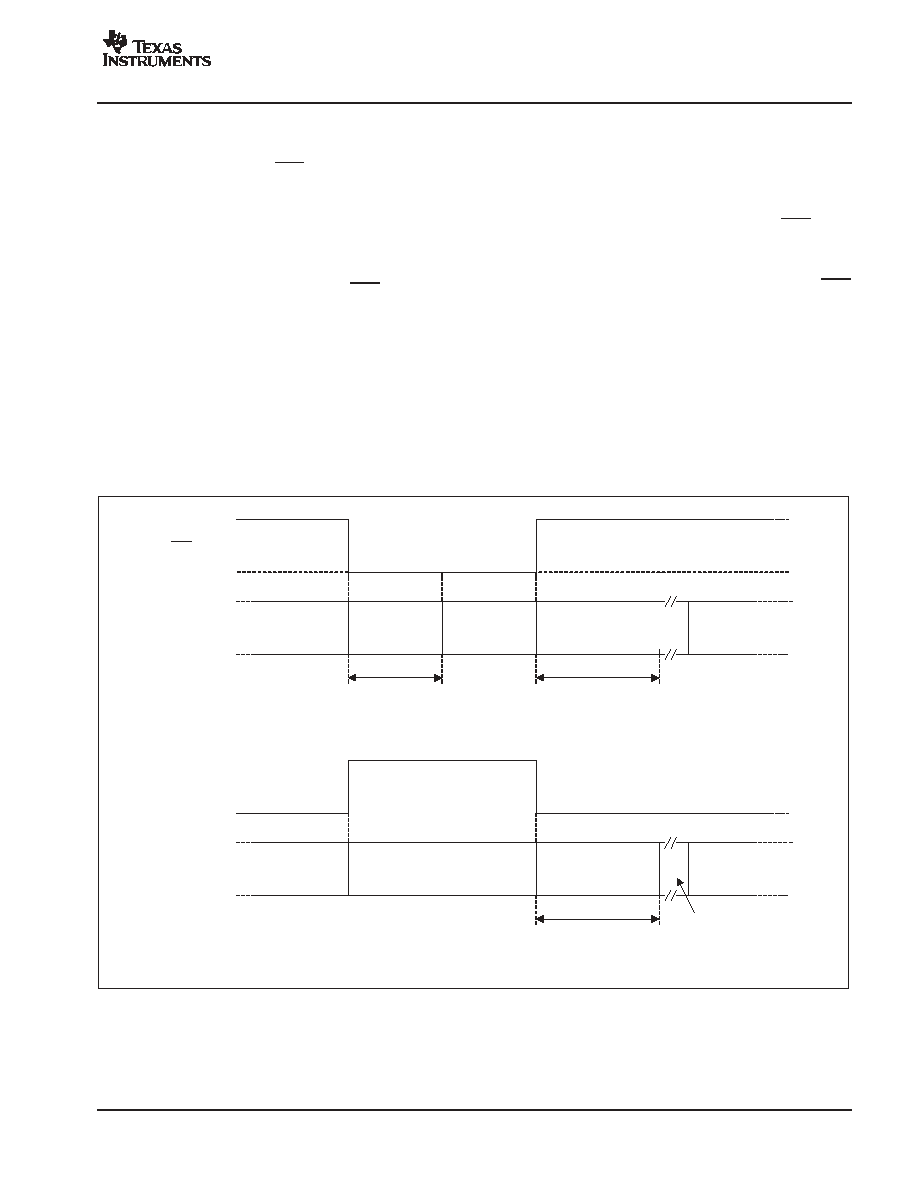
Figure 10. Left-Justified, Right-Justified, and I
2
S Data Formats
LRCK
BCK
(BCKE = 0)
t
DS
t
DH
t
BKLRD
BCK
(BCKE = 1)
t
LRBKD
t
BCKP
t
BCKHL
P A R A M E TE R
D E S C R IP T IO N
M IN
M A X
U N ITS
70
ns
30
ns
10
ns
10
ns
10
ns
10
ns
50
%
BCK Cycle Time
BCK High/Low Time
LRCK Edge to BCK Sampling Edge Delay
BCK Sampling Edge to LRCK Edge Delay
Data Setup Time
Data Hold Time
LRCK Duty Cycle
t
BCKP
t
BCKHL
t
LRBKD
t
BKLRD
t
DS
t
DH
-
Audio Data
Figure 11. Audio Serial Port Timing for Left-Justified, Right-Justified, and I
2
S Data Formats
PRODUCT PREVIEW
PCM4108
SBAS354 - JUNE 2005
www.ti.com
22
SUBA
DGND
V
DD
PCM4108
(a) TDM Formats, Single or Dual Rate Sampling Modes.
SUBB
Ch. 1-8
LRCK
BCK
DATA0
DATA2
DSP
Decoder,
or Logic
SCKI
Clock
SUBA
DGND
PCM4108
(b) TDM Formats, Quad Rate Sampling Mode.
SUBB
Ch. 1-4
Ch. 5-8
LRCK
BCK
DATA0
DATA2
DSP
Decoder,
or Logic
SCKI
Clock
Figure 12. TDM Connection
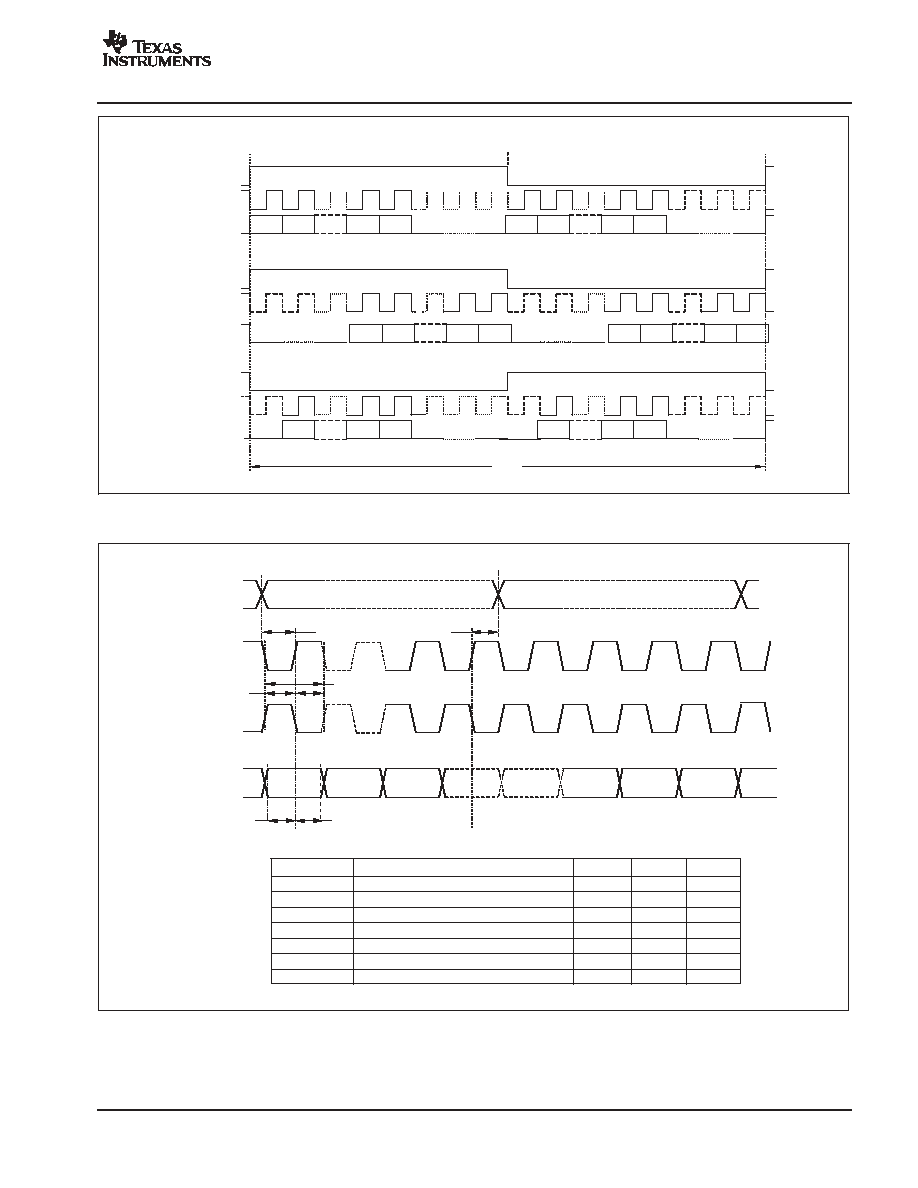
LRCK
Normal, Zero BCK Delay
LRCK
Normal, One BCK Delay
LRCK
Inverted, Zero BCK Delay
LRCK
Inverted, One BCK Delay
Audio Data applied
to both DATA0 and DATA2
Slot 1
Slot 2
Slot 3
Slot 4
Slot 5
Slot 6
Slot 7
Slot 8
Ch. 1
Ch. 2
Ch. 3
Ch. 4
Ch. 5
Ch. 6
Ch. 7
Ch. 8
Sub-Frame 0
(SUBA = 0)
Sub-Frame 1
(SUBB = 1)
One Frame
BCK = 192f
S
or 256f
S
In the case of BCK = 192f
S
, each time slot is 24 bits long and contains the 24-bit audio data for the corresponding channel.
In the case of BCK = 256f
S
, each time slot is 32 bits long and contains the 24-bit audio data for the corresponding channel.
The audio data is left justified in the time slot, with the least significant 8 bits of each time slot being don't care bits.
Audio data is always presented in two's complement, MSB-first format.
TDM Data Formats
-
Single and Dual Rate Sampling Modes
Figure 13. TDM Data Formats: Single and Dual Rate Sampling Modes
PRODUCT PREVIEW
PCM4108
SBAS354 - JUNE 2005
www.ti.com
23
Slot 1
Slot 2
Slot 3
Slot 4
Ch. 1
Ch. 2
Ch. 3
Ch. 4
In the case of BCK = 96f
S
, each time slot is 24 bits long and contains the 24-bit audio data for the corresponding channel.
In the case of BCK = 128f
S
, each time slot is 32 bits long and contains the 24-bit audio data for the corresponding channel.
The audio data is left justified in the time slot, with the the least significant 8 bits of each time slot being don't care bits.
Audio data is always presented in two's complement, MSB-first format.
LRCK
Normal, Zero BCK Delay
LRCK
Normal, One BCK Delay
LRCK
Inverted, Zero BCK Delay
LRCK
Inverted, One BCK Delay
DATA0
DATA2
Ch. 5
Ch. 6
Ch. 7
Ch. 8
One Frame
BCK = 96f
S
or 128f
S
(SUBA = SUBB = 0)
TDM Data Formats
-
Quad Rate Sampling Mode
Figure 14. TDM Data Formats: Quad Rate Sampling Mode
LRCK
BCK
(BCKE = 0)
t
DS
t
DH
t
LRBKD
t
LRCKP
t
BNF
t
BKBF
One Frame
BCK
(BCKE = 1)
P A R A M E T E R
D E S C R IP T IO N
M IN
M A X
U N IT S
1/f
BCK
1/f
BCK
12
10
10
12
ns
ns
ns
ns
ns
ns
t
LRCKP
t
LRBKD
t
DS
t
DH
t
BNF
t
BKBF
LRCK pulse width
LRCK active edge to BCK sampling edge delay
Data setup time
Data hold time
LRCK transition before new frame
BCK sampling edge to new frame delay
Audio Data
Figure 15. TDM Timing
PRODUCT PREVIEW
PCM4108
SBAS354 - JUNE 2005
www.ti.com
24
STANDALONE MODE CONFIGURATION
Standalone mode is selected by forcing the MODE input
(pin 12) low. Standalone mode operation provides a
subset of the functions available in Software mode, while
providing an option for a simplified control model.
Standalone configuration is accomplished by either
hardwiring or driving a small set of input pins with external
logic or switches. Standalone mode functions include
sampling mode and audio data format selection, an
all-channel soft mute function, and digital de-emphasis
filtering. The following paragraphs provide a brief
description of each function available when using
Standalone mode.
Sampling Mode
The sampling mode is selected using the FS0 (pin 36) and
FS1 (pin 37) inputs. A more detailed discussion of the
sampling modes was provided in an earlier section of this
data sheet. Table 2 summarizes the sampling mode
configuration for Standalone mode.
Table 2. Sampling Mode Configuration
FS1
FS0
SAMPLING MODE
0
0
Single Rate
0
1
Dual Rate
1
0
Quad Rate
1
1
- Not Used -
Audio Data Format
The audio data format is selected using the FMT0 (pin 33),
FMT1 (pin 34), and FMT2 (pin 35) inputs. A detailed
discussion of the audio serial port operation and the
corresponding data formats was provided in the Audio
Serial Port section on pages 20 through 23. For
Standalone mode, the LRCK polarity is always normal,
while the serial audio data is always sampled on the rising
edge of the BCK clock. Table 3 shows the audio data
format configuration for Standalone mode.
Table 3. Audio Data Format Configuration
FMT2
FMT1
FMT0
AUDIO DATA FORMAT
0
0
0
24-bit, left-justified
0
0
1
24-bit I2S
0
1
0
TDM with zero BCK delay
0
1
1
TDM with one BCK delay
1
0
0
24-bit, right-justified
1
0
1
20-bit, right-justified
1
1
0
18-bit, right-justified
1
1
1
16-bit, right-justified
Soft Mute Function
The MUTE input (pin 14) may be used in either the
Standalone or Software modes to simultaneously mute the
eight output channels. The soft mute function slowly ramps
the digital output attenuation from its current setting to the
mute level, minimizing or eliminating audible artifacts.
Table 4 summarizes MUTE function operation.
Table 4. Mute Function Configuration
MUTE
ANALOG OUTPUTS
0
On (mute disabled)
1
Muted
Digital De-Emphasis
This is a global digital function (common to all eight
channels) and provides de-emphasis of the higher
frequency content within the 20kHz audio band.
De-emphasis is required when the input audio data has
been pre-emphasized. Pre-emphasis entails increasing
the amplitude of the higher frequency components in the
20kHz audio band using a standardized filter function in
order to enhance the high-frequency response. The
PCM4108 de-emphasis filters implement the standard
50/15
µ
s de-emphasis transfer function commonly used in
digital audio applications.
De-emphasis filtering is available for three input sampling
frequencies in Single Rate sampling mode: 32kHz,
44.1kHz, and 48kHz. De-emphasis is not available when
operating in Dual or Quad Rate sampling modes. The
de-emphasis filter is selected using the DEM0 (pin 16) and
DEM1 (pin 15) inputs. Table 5 illustrates the de-emphasis
filter configuration for Standalone mode.
Table 5. Digital De-Emphasis Configuration
DEM1
DEM0
DIGITAL DE-EMPHASIS MODE
0
0
Off (de-emphasis disabled)
0
1
48kHz
1
0
44.1kHz
1
1
32kHz
PRODUCT PREVIEW

PCM4108
SBAS354 - JUNE 2005
www.ti.com
25
SOFTWARE MODE CONFIGURATION
Software mode is selected by forcing the MODE input
(pin 12) high. Software mode operation provides full
access to the features of the PCM4108 by allowing the
writing and reading of on-chip control registers. This is
accomplished using the five-wire SPI port. The following
paragraphs provide a brief description of each function
available when using Software mode.
Digital Attenuation
The audio signal for each channel can be attenuated in the
digital domain using this function. Attenuation settings
from 0dB (unity gain) to -119.5dB are provided in 0.5dB
steps. In addition, the attenuation level may be set to the
mute state. The rate of change for the digital attenuation
function is one 0.5dB step for every eight LRCK periods.
Each channel has its own independent attenuation control,
accessed using control registers 1 through 4 in Banks A
and B. The reset default setting for all channels is 0dB, or
unity gain (no attenuation applied).
Digital De-Emphasis
The de-emphasis function is accessed through Control
Register 5 in Banks A and B using the DEM[1:0] bits. The
reset default setting is that the de-emphasis is disabled for
all four channels in each bank. De-emphasis filter
operation is described in the Standalone Mode
Configuration section of this data sheet.
Soft Mute
Each of the eight D/A converter channels has its own
independent soft mute control, located in Control Register
5, for Banks A and B.
The reset default is normal output for all eight channels
with the soft mute function disabled. The MUTE input (pin
14) also functions in Software mode, with a high input
forcing soft mute on all eight channels.
Zero Data Mute
The PCM4108 includes a zero data detection and mute
function in Software mode. This function automatically
mutes a given channel when 1024 consecutive LRCK
periods of all zero data are detected for that channel. The
zero data mute function is enabled and disabled using the
ZDM bit in Control Register 5 for Banks A and B. The zero
data mute function is disabled by default on power up or
reset.
Output Phase Reversal
The PCM4108 includes an output phase reversal function,
which provides the ability to invert the output phase for all
eight channels, either for testing or for matching various
output circuit configurations. This function is controlled
using the PHASE bit, located within Control Register 5, for
Banks A and B. The output phase is set to noninverted by
default on power up or reset.
Sampling Mode
Sampling mode configuration was discussed earlier in this
data sheet, with Table 1 providing a reference for common
sampling and system clock frequencies. The FS0 and FS1
bits located in Control Register 6 for Banks A and B. The
sampling made must be the same for both banks are used
to set the sampling mode. The sampling mode defaults to
Single Rate on power up or reset.
Power-Down Modes
The power-down control bits are located in Control
Register 6 for each bank. These bits are used to power
down pairs of D/A converters within the PCM4108. When
a channel pair is powered down, it ignores the audio data
inputs and sets its outputs to a high-impedance state. By
default, the power-down bits are disabled on power up or
reset.
Software Reset
This reset function allows a reset sequence to be initiated
under software control. All control registers are reset to
their default state. The reset bit, RST, is located in Control
Register 6, for Banks A and B. Setting this bit to 1 initiates
a one-time reset sequence. The RST bit is cleared by the
initialization sequence.
Audio Data Formats, LRCK Polarity, and BCK
Sampling Edge
Control Register 7 in Banks A and B is used to configure
the PCM4108 audio serial port. Audio serial port operation
was discussed previously in this data sheet. The control
register definitions provide additional information
regarding the register functions and their default settings.
PRODUCT PREVIEW
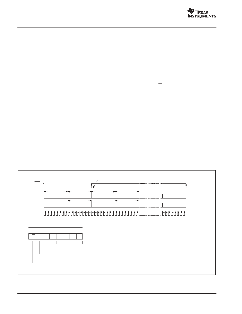
PCM4108
SBAS354 - JUNE 2005
www.ti.com
26
SERIAL PERIPHERAL INTERFACE (SPI) PORT
OPERATION
The SPI port is a five-wire synchronous serial interface that
is used to access the on-chip control registers when the
PCM4108 is configured for Software mode operation. The
CDIN input (pin 31) is the serial data input for the port, while
CDOUT (pin 32) is used for reading back control register
contents in a serial fashion. The CSA (pin 28) and CSB (pin
29) inputs function as the chip selects for register Banks
A and B, respectively. The CCLK input (pin 30) functions
as the serial data clock, used to clock data in and out of the
port. Data is clocked into the port on the rising edge of
CCLK, while data is clocked out of the port on the falling
edge of CCLK.
There are three modes of operation supported for the SPI
port: Single Register, Continuous, and Auto-Increment.
The Single Register and Continuous modes are similar to
one another. In Continuous mode, instead of bringing the
chip select input high after writing or reading a single
register, the chip select input is held low and a new control
byte is issued with a new address for the next write or read
operation. Continuous mode allows multiple, sequential or
nonsequential register addresses to be read or written in
succession, as shown in Figure 16.
Auto-Increment mode is designed for writing or reading
multiple sequential register addresses. After the first
register is written or read, the register address is
automatically incremented by 1, so the next write or read
operation is performed without issuing another control
byte, as shown in Figure 17.
Control Byte (or Byte 0)
The control byte, or byte `0', is the first byte written to the
PCM4108 SPI port when performing a write or read
operation. The control byte includes bits that define the
operation to be performed (read or write), the
auto-increment mode status, and the control register
address.
The Read/Write bit, R/W, is set to `0' to indicate a register
write operation, or set to 1 for a register read operation.
The Increment bit, INC, enables or disables the
Auto-Increment mode of operation. When this bit is set to
a `0', auto-increment operation is disabled, and the
operation performed is either Single Register or
Continuous. Setting the INC bit to `1' enables
Auto-Increment operation.
A two-bit key code, 10
B
, follows the INC bit and must be
present in order for any operation to take place on the
control port. Any other combination for these bits will result
in the port ignoring the write or read request.
The four-bit address field, A[3:0], is used to specify the
control register address for the read or write operation, or
the starting address for an Auto-Increment write or read
operation.
CSA
CSB
CDIN
CCLK
Keep CSA and/or CSB low for writing or reading multiple registers in Continuous mode
byte 0
byte 1
byte 0
byte 1
byte N
Auto-Increment Control: Set to 0 for Single Register or Continuous Operation
Read/WriteControl: 0 = Write
1 = Read
Register Data
Control Byte
Register Data
Control Byte
CDOUT
High Impedance
byte 1
High Impedance
byte 2
byte N
Register Data
Register Data
R/W INC
1
0
A3
A2
A1
A0
Register Address
MSB
LSB
Control Byte Definition (Byte 0)
Figure 16. Single Register and Continuous Write or Read Operation
PRODUCT PREVIEW

PCM4108
SBAS354 - JUNE 2005
www.ti.com
27
CSA
CSB
CDIN
CCLK
byte 0
byte 1
byte 2
byte 3
byte N
R/W INC
1
0
A3
A2
A1
A0
Auto-Increment Control: Set to 1 for Auto-Increment Operation
Read/WriteControl: 0 = Write
1 = Read
MSB
LSB
Control Byte Definition (Byte 0)
Register Data
Register Data
Control Byte
CDOUT
High Impedance
byte 1
byte 2
byte 3
byte N
Register Address
Register Data
Register Data
Register Data
Register Data
Register Data
Figure 17. Auto-Increment Write or Read Operation
High Impedance (Hi Z)
Hi Z
CSA
CSB
CCLK
CDIN
CDOUT
MSB
MSB
LSB
t
DO
t
DS
t
DH
t
CH
t
CSZ
PARAMETER
DESCRIPTION
MIN
MAX
UNIT
CDIN Data Setup Time
5
2
2
5
5
ns
CDIN Data Hold Time
ns
CS Hold Time
ns
CDOUT Data Delay Time
ns
CS High to CDOUT Hi Z
t
DS
t
DH
t
CH
t
DO
t
CSZ
ns
Figure 18. SPI Port Timing
PRODUCT PREVIEW
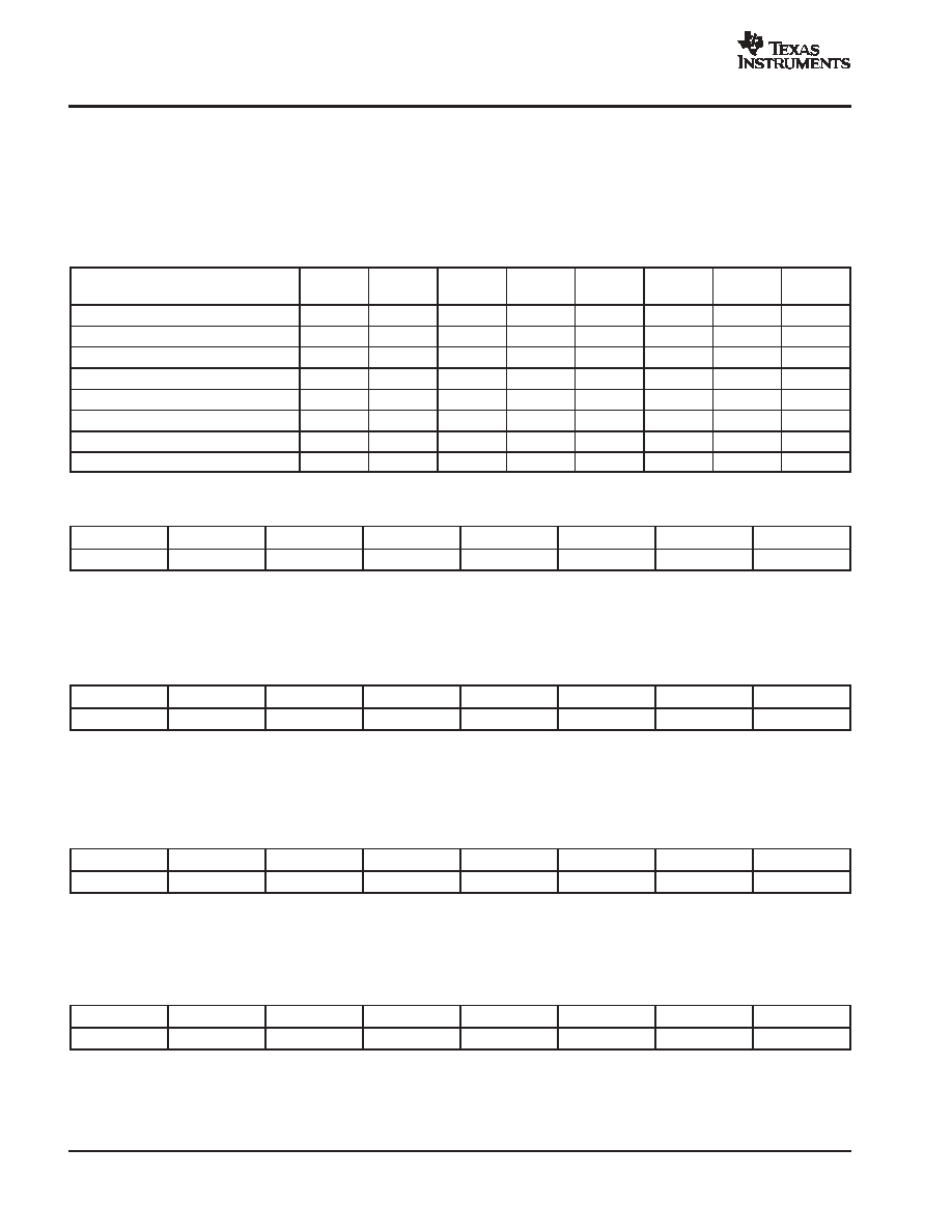
PCM4108
SBAS354 - JUNE 2005
www.ti.com
28
CONTROL REGISTER DEFINITIONS (SOFTWARE MODE ONLY)
The PCM4108 includes a small set of control registers, which are utilized to configure the full set of on-chip functions in
Software mode. The register maps for register Banks A and B are shown in Table 6 and Table 7, respectively. Register 0
is reserved for factory use and should not be written to for normal operation. Register 0 defaults to all zero data on power
up or reset.
Table 6. Control Register Map for Bank A
CONTROL REGISTER ADDRESS
(HEX)
MSB
BIT 7
BIT 6
BIT 5
BIT 4
BIT 3
BIT 2
BIT 1
LSB
BIT 0
0
0
0
0
0
0
0
0
0
1
AT17
AT16
AT15
AT14
AT13
AT12
AT11
AT10
2
AT27
AT26
AT25
AT24
AT23
AT22
AT21
AT20
3
AT37
AT36
AT35
AT34
AT33
AT32
AT31
AT30
4
AT47
AT46
AT45
AT44
AT43
AT42
AT41
AT40
5
MUT4
MUT3
MUT2
MUT1
ZDM
PHASE
DEM1
DEM0
6
RST
0
0
0
PDN34
PDN12
FS1
FS0
7
0
0
BCKE
LRCKP
0
FMT2
FMT1
FMT0
Register 1: Attenuation Control Register - Channel 1
BIT 7 (MSB)
BIT 6
BIT 5
BIT 4
BIT 3
BIT 2
BIT 1
BIT 0 (LSB)
AT17
AT16
AT15
AT14
AT13
AT12
AT11
AT10
This register controls the digital output attenuation for
Channel 1.
Default: AT1[7:0] = 255, or 0dB
Let N = AT1[7:0].
For N = 16 to 255, Attenuation (dB) = 0.5 x (255 ≠ N)
For N = 0 to 15, Attenuation (dB) = Infinite (Muted)
Register 2: Attenuation Control Register ≠ Channel 2
BIT 7 (MSB)
BIT 6
BIT 5
BIT 4
BIT 3
BIT 2
BIT 1
BIT 0 (LSB)
AT27
AT26
AT25
AT24
AT23
AT22
AT21
AT20
This register controls the digital output attenuation for
Channel 2.
Default: AT2[7:0] = 255, or 0dB
Let N = AT2[7:0].
For N = 16 to 255, Attenuation (dB) = 0.5 x (255 ≠ N)
For N = 0 to 15, Attenuation (dB) = Infinite (Muted)
Register 3: Attenuation Control Register ≠ Channel 3
BIT 7 (MSB)
BIT 6
BIT 5
BIT 4
BIT 3
BIT 2
BIT 1
BIT 0 (LSB)
AT37
AT36
AT35
AT34
AT33
AT32
AT31
AT30
This register controls the digital output attenuation for
Channel 3.
Default: AT3[7:0] = 255, or 0dB
Let N = AT3[7:0].
For N = 16 to 255, Attenuation (dB) = 0.5 x (255 ≠ N)
For N = 0 to 15, Attenuation (dB) = Infinite (Muted)
Register 4: Attenuation Control Register ≠ Channel 4
BIT 7 (MSB)
BIT 6
BIT 5
BIT 4
BIT 3
BIT 2
BIT 1
BIT 0 (LSB)
AT47
AT46
AT45
AT44
AT43
AT42
AT41
AT40
This register controls the digital output attenuation for
Channel 4.
Default: AT4[7:0] = 255, or 0dB
Let N = AT4[7:0].
For N = 16 to 255, Attenuation (dB) = 0.5 x (255 ≠ N)
For N = 0 to 15, Attenuation (dB) = Infinite (Muted)
PRODUCT PREVIEW
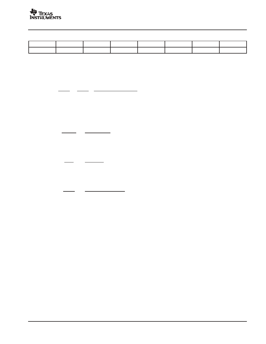
PCM4108
SBAS354 - JUNE 2005
www.ti.com
29
Register 5: Function Control Register
BIT 7 (MSB)
BIT 6
BIT 5
BIT 4
BIT 3
BIT 2
BIT 1
BIT 0 (LSB)
MUT4
MUT3
MUT2
MUT1
ZDM
PHASE
DEM1
DEM0
This register controls various D/A converter functions, including de-emphasis filtering, output phase reversal, zero data
mute, and per-channel soft muting.
DEM[1:0]
Digital De-Emphasis for Channels 1 through 4
De-emphasis is available for Single Rate mode only. De-emphasis is disabled for Dual and Quad Rate modes.
DEM1
DEM0
De-Emphasis Selection
0
0
De-emphasis disabled (default)
0
1
De-emphasis for f
S
= 48kHz
1
0
De-emphasis for f
S
= 44.1kHz
1
1
De-emphasis for f
S
= 32kHz
PHASE
Output Phase for Channels 1 through 4
PHASE
Output Phase
0
Noninverted (default)
1
Inverted
ZDM
Zero Data Mute for Channels 1 through 4
ZDM
Zero Mute
0
Disabled (default)
1
Enabled
MUT[4:1]
Soft Mute for Channels 1 through 4
MUTx
D/A Converter Output
0
On (default)
1
Muted
NOTE: x = channel number.
PRODUCT PREVIEW
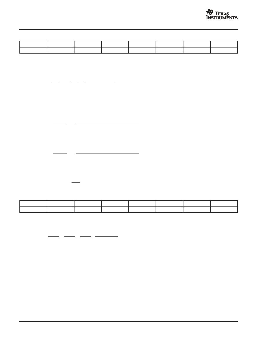
PCM4108
SBAS354 - JUNE 2005
www.ti.com
30
Register 6: System Control Register
BIT 7 (MSB)
BIT 6
BIT 5
BIT 4
BIT 3
BIT 2
BIT 1
BIT 0 (LSB)
RST
0
0
0
PDN34
PDN12
FS1
FS0
This register controls various system level functions of the PCM4108, including sampling mode, power-down, and soft
reset.
FS[1:0]
Sampling Mode for Channels 1 through 4
FS1
FS0
Sampling Mode
0
0
Single Rate (default)
0
1
Dual Rate
1
0
Quad Rate
1
1
- Not Used -
PDN12
Power-Down for Channels 1 and 2
PDN12
Power Down for Channels 1 and 2
0
Disabled (default)
1
Enabled
PDN34
Power-Down for Channels 3 and 4
PDN34
Power Down for Channels 3 and 4
0
Disabled (default)
1
Enabled
RST
Software Reset (value defaults to 0) for Channels 1 through 4
Setting this bit to `1' will initiate a logic reset of the PCM4108. This bit functions the same as an external reset
applied at the RST input (pin 13).
Register 7: Audio Serial Port Control Register for Channels 1 through 4
BIT 7 (MSB)
BIT 6
BIT 5
BIT 4
BIT 3
BIT 2
BIT 1
BIT 0 (LSB)
0
0
BCKE
LRCKP
0
FMT2
FMT1
FMT0
This register is used to control the data format and clock polarity for the PCM4108 audio serial port.
FMT[2:0]
Audio Data Format
FMT2
FMT1
DEM0
Data Format
0
0
0
24-bit, left-justified (default)
0
0
1
24-bit I
2
S
0
1
0
TDM with zero BCK delay
0
1
1
TDM with one BCK delay
1
0
0
24-bit, right-justified
1
0
1
20-bit, right-justified
1
1
0
18-bit, right-justified
1
1
1
16-bit, right-justified
LRCKP
LRCK Polarity (0 = Normal, 1 = Inverted). Defaults to 0.
BCKE
BCK Sampling Edge (0 = Rising Edge, 1 = Falling Edge), Defaults to 0.
PRODUCT PREVIEW

PCM4108
SBAS354 - JUNE 2005
www.ti.com
31
Table 7. Control Register Map for Bank B
CONTROL REGISTER ADDRESS
(HEX)
MSB
BIT 7
BIT 6
BIT 5
BIT 4
BIT 3
BIT 2
BIT 1
LSB
BIT 0
0
0
0
0
0
0
0
0
0
1
AT57
AT56
AT55
AT54
AT53
AT52
AT51
AT50
2
AT67
AT66
AT65
AT64
AT63
AT62
AT61
AT60
3
AT77
AT76
AT75
AT74
AT73
AT72
AT71
AT70
4
AT87
AT86
AT85
AT84
AT83
AT82
AT81
AT80
5
MUT8
MUT7
MUT6
MUT5
ZDM
PHASE
DEM1
DEM0
6
RST
0
0
0
PDN78
PDN56
FS1
FS0
7
0
0
BCKE
LRCKP
0
FMT2
FMT1
FMT0
Register 1: Attenuation Control Register - Channel 5
BIT 7 (MSB)
BIT 6
BIT 5
BIT 4
BIT 3
BIT 2
BIT 1
BIT 0 (LSB)
AT57
AT56
AT55
AT54
AT53
AT52
AT51
AT50
This register controls the digital output attenuation for
Channel 5.
Default: AT5[7:0] = 255, or 0dB
Let N = AT5[7:0].
For N = 16 to 255, Attenuation (dB) = 0.5 x (255 ≠ N)
For N = 0 to 15, Attenuation (dB) = Infinite (Muted)
Register 2: Attenuation Control Register ≠ Channel 6
BIT 7 (MSB)
BIT 6
BIT 5
BIT 4
BIT 3
BIT 2
BIT 1
BIT 0 (LSB)
AT67
AT66
AT65
AT64
AT63
AT62
AT61
AT60
This register controls the digital output attenuation for
Channel 6.
Default: AT6[7:0] = 255, or 0dB
Let N = AT6[7:0].
For N = 16 to 255, Attenuation (dB) = 0.5 x (255 ≠ N)
For N = 0 to 15, Attenuation (dB) = Infinite (Muted)
Register 3: Attenuation Control Register ≠ Channel 7
BIT 7 (MSB)
BIT 6
BIT 5
BIT 4
BIT 3
BIT 2
BIT 1
BIT 0 (LSB)
AT77
AT76
AT75
AT74
AT73
AT72
AT71
AT70
This register controls the digital output attenuation for
Channel 7.
Default: AT7[7:0] = 255, or 0dB
Let N = AT7[7:0].
For N = 16 to 255, Attenuation (dB) = 0.5 x (255 ≠ N)
For N = 0 to 15, Attenuation (dB) = Infinite (Muted)
Register 4: Attenuation Control Register ≠ Channel 8
BIT 7 (MSB)
BIT 6
BIT 5
BIT 4
BIT 3
BIT 2
BIT 1
BIT 0 (LSB)
AT87
AT86
AT85
AT84
AT83
AT82
AT81
AT80
This register controls the digital output attenuation for
Channel 8.
Default: AT8[7:0] = 255, or 0dB
Let N = AT8[7:0].
For N = 16 to 255, Attenuation (dB) = 0.5 x (255 ≠ N)
For N = 0 to 15, Attenuation (dB) = Infinite (Muted)
PRODUCT PREVIEW
PCM4108
SBAS354 - JUNE 2005
www.ti.com
32
Register 5: Function Control Register
BIT 7 (MSB)
BIT 6
BIT 5
BIT 4
BIT 3
BIT 2
BIT 1
BIT 0 (LSB)
MUT8
MUT7
MUT6
MUT5
ZDM
PHASE
DEM1
DEM0
This register controls various D/A converter functions, including de-emphasis filtering, output phase reversal, zero data
mute, and per-channel soft muting.
DEM[1:0]
Digital De-Emphasis for Channels 5 through 8
De-emphasis is available for Single Rate mode only. De-emphasis is disabled for Dual and Quad Rate modes.
DEM1
DEM0
De-Emphasis Selection
0
0
De-emphasis disabled (default)
0
1
De-emphasis for f
S
= 48kHz
1
0
De-emphasis for f
S
= 44.1kHz
1
1
De-emphasis for f
S
= 32kHz
PHASE
Output Phase for Channels 5 through 8
PHASE
Output Phase
0
Noninverted (default)
1
Inverted
ZDM
Zero Data Mute for Channels 5 through 8
ZDM
Zero Mute
0
Disabled (default)
1
Enabled
MUT[4:1]
Soft Mute for Channels 5 through 8
MUTx
D/A Converter Output
0
On (default)
1
Muted
NOTE: x = channel number.
PRODUCT PREVIEW

PCM4108
SBAS354 - JUNE 2005
www.ti.com
33
Register 6: System Control Register
BIT 7 (MSB)
BIT 6
BIT 5
BIT 4
BIT 3
BIT 2
BIT 1
BIT 0 (LSB)
RST
0
0
0
PDN78
PDN56
FS1
FS0
This register controls various system level functions of the PCM4108, including sampling mode, power-down, and soft
reset.
FS[1:0]
Sampling Mode for Channels 5 through 8
FS1
FS0
Sampling Mode
0
0
Single Rate (default)
0
1
Dual Rate
1
0
Quad Rate
1
1
- Not Used -
PDN56
Power-Down for Channels 5 and 6
PDN12
Power Down for Channels 5 and 6
0
Disabled (default)
1
Enabled
PDN78
Power-Down for Channels 7 and 8
PDN34
Power Down for Channels 7 and 8
0
Disabled (default)
1
Enabled
RST
Software Reset (value defaults to 0) for Channels 5 through 8
Setting this bit to 1 will initiate a logic reset of the PCM4108. This bit functions the same as an external reset
applied at the RST input (pin 13).
Register 7: Audio Serial Port Control Register for Channels 5 through 8
BIT 7 (MSB)
BIT 6
BIT 5
BIT 4
BIT 3
BIT 2
BIT 1
BIT 0 (LSB)
0
0
BCKE
LRCKP
0
FMT2
FMT1
FMT0
This register is used to control the data format and clock polarity for the PCM4108 audio serial port.
FMT[2:0]
Audio Data Format
FMT2
FMT1
DEM0
Data Format
0
0
0
24-bit, left-justified (default)
0
0
1
24-bit I
2
S
0
1
0
TDM with zero BCK delay
0
1
1
TDM with one BCK delay
1
0
0
24-bit, right-justified
1
0
1
20-bit, right-justified
1
1
0
18-bit, right-justified
1
1
1
16-bit, right-justified
LRCKP
LRCK Polarity (0 = Normal, 1 = Inverted). Defaults to 0.
BCKE
BCK Sampling Edge (0 = Rising Edge, 1 = Falling Edge), Defaults to 0.
PRODUCT PREVIEW

PCM4108
SBAS354 - JUNE 2005
www.ti.com
34
APPLICATIONS INFORMATION
This section provides practical information for system and
hardware engineers that are designing in the PCM4108.
BASIC CIRCUIT CONFIGURATIONS
Figure 19 shows a typical circuit configuration for the
PCM4108 operated in Standalone and Software modes.
Power supply bypass and reference decoupling
capacitors should be placed as close to the corresponding
PCM4108 pins as possible. Separate power supplies are
utilized for the analog and digital sections, with +5V
required for the PCM4108 analog supplies and +3.3V
required for the digital supply.
The +5V analog supply may be derived from a higher
valued, positive analog power supply using a linear
voltage regulator, such as the REG103 available from
Texas Instruments. The +3.3V digital supply can be
derived from a primary +5V digital supply using a linear
voltage regulator, such as the REG1117, also from TI. The
PCM4108EVM evaluation module provides an example of
how the common ground with separate supply approach
can be successfully implemented. The PCM4108EVM
User's Guide includes schematics and PCB layout plots
for reference. The evaluation module is available through
Texas Instruments' distributors and sales representatives,
or may be ordered online through the TI eStore, which can
be accessed through the TI home page at
http://www.ti.com
.
The master clock generator supplies the system clock for
the PCM4108, as well as the audio data source, such as
a digital signal processor. The LRCK and BCK audio
clocks should be derived from the system clock, in order
to ensure synchronous operation.
ANALOG OUTPUT FILTER CIRCUITS
An external output filter is recommended for each
differential output pair. The external output filter further
reduces the out-of-band noise energy produced by the
delta-sigma modulator, while providing band limiting
suitable for audio reproduction. A 2nd-order Butterworth
low-pass filter circuit with a -3dB corner frequency from
50kHz to 180kHz is recommended.
The configuration of the output filter circuit depends on
whether a single-ended or differential output is required.
Single-ended outputs are commonly used in consumer
playback systems, while differential or balanced outputs
are used in many professional audio applications, such as
recording or broadcast studios and live sound systems.
Figure 20 illustrates an active filter circuit that uses a single
op amp to provide both 2nd-order low-pass filtering and
differential to single-ended signal conversion. This circuit
is used on the PCM4108EVM evaluation module and
meets the published typical Electrical Characteristics for
dynamic performance. The single-ended output is
convenient for connecting to both headphone and power
amplifiers when used for listening tests.
The quality of the op amp used is this circuit is important,
as many devices will degrade the dynamic range and/or
total harmonic distortion plus noise (THD+N)
specifications for the PCM4108. An NE5534A is shown in
Figure 20 and provides both low noise and distortion.
Bipolar input op amps with equivalent specifications
should produce similar measurement results. Devices that
exhibit higher equivalent input noise voltage, such as the
Texas Instruments OPA134 or OPA604 families, will
produce lower dynamic range measurements
(approximately 1dB to 2dB lower than the typical
PCM4108 specification), while having little or no impact on
the THD+N specification when measuring a full-scale
output level.
Figure 21 illustrates a fully-differential output filter circuit
suitable for use with the PCM4108. The OPA1632 from
Texas Instruments provides the fully differential signal path
in this circuit. The OPA1632 features very low noise and
distortion, making it suitable for high-end audio
applications.
Texas Instruments provides a free software tool,
FilterPro
t
, used to assist in the design of active filter
circuits. The software supports design of multiple
feedback (MFB), Sallen-Key, and fully differential filter
circuits. FilterPro is available from the TI web site.
Additionally, TI document number SBAF001A, also
available from the TI web site, provides pertinent
application information regarding the proper usage of the
FilterPro program.
PRODUCT PREVIEW
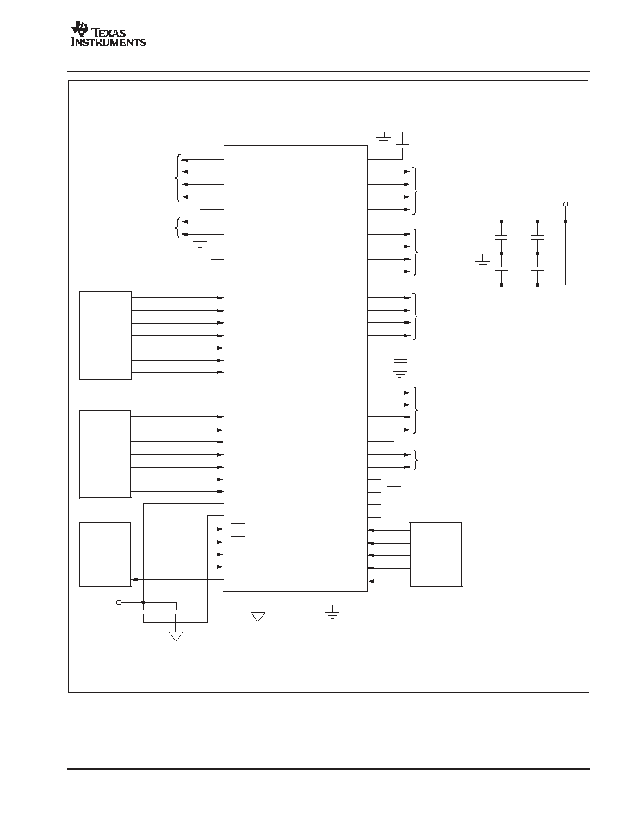
PCM4108
SBAS354 - JUNE 2005
www.ti.com
35
1
2
3
4
5
6
7
8
9
10
11
12
13
14
15
16
17
18
V
OUT
1+
V
OUT
1
-
V
OUT
5+
V
OUT
5
-
AGND1
V
REF
1
-
V
REF
1+
NC
NC
NC
NC
MODE
RST
MUTE
DEM1
DEM0
SUBA
SUBB
Control
Logic
To Output Filters
(see Figures 20 and 21)
To Decoupling Capacitors
(see Figure 3)
+3.3V
Digital
10
µ
F
0.1
µ
F
+
19
20
21
22
23
24
25
26
27
28
29
30
31
32
SCKI
BCK
LRCK
DATA0
DATA1
DATA2
DATA3
V
DD
DGND
CSA
CSB
CCLK
CDIN
CDOUT
Audio
Processor
(DSP)
SPI HOST
(MCU, FPGA)
64
63
62
61
60
59
58
57
56
55
54
53
52
51
50
49
V
COM
1
V
OUT
2+
V
OUT
2
-
V
OUT
6+
V
OUT
6
-
V
CC
1
V
REF
4+
V
REF
4
-
V
REF
3
-
V
REF
3+
V
CC
2
V
OUT
3
-
V
OUT
3+
V
OUT
7
-
V
OUT
7+
V
COM
2
Control
Logic
0.1
µ
F
10
µ
F
+
0.1
µ
F
10
µ
F
+
0.1
µ
F
0.1
µ
F
48
47
46
45
44
43
42
41
40
39
38
37
36
35
34
33
V
OUT
4+
V
OUT
4
-
V
OUT
8+
V
OUT
8
-
AGND2
V
REF
2
-
V
REF
2+
NC
NC
NC
NC
FS1
FS0
FMT2
FMT1
FMT0
To Output Filters
(see Figures 20 and 21)
To Decoupling Capacitors
(see Figure 3)
To Output Filters
(see Figures 20 and 21)
To Decoupling
Capacitors
(see Figure 3)
To Output Filters
(see Figures 20 and 21)
+5V
Analog
PCM4108
Figure 19. Typical Connection Diagram
PRODUCT PREVIEW
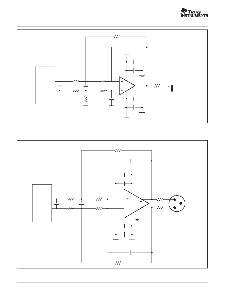
PCM4108
SBAS354 - JUNE 2005
www.ti.com
36
499
604
1k
100
Filtered
Output
RCA or 1/4-inch
Phone Jack
NE5534A
PCM4108
560pF
499
1k
560pF
604
2200pF
22pF
0.1
µ
F
10
µ
F
+12V
VOUTn
-
VOUTn+
n = 1, 2, 3, 4, 5, 6, 7, or 8
2
3
7
6
4
10
µ
F
0.1
µ
F
-
12V
+
+
Figure 20. Single-Ended Output Filter Circuit
499
604
100
100
1k
1k
Filtered
Output
Male XLR
Connector
OPA1632
PCM4108
560pF
560pF
499
604
2200pF
22pF
0.01
µ
F
10
µ
F
-
15V
VOUTn
-
VOUTn+
n = 1, 2, 3, 4, 5, 6, 7, or 8
2
1
8
EN
V
OCM
2
3
1
7
6
3
4
5
10
µ
F
0.01
µ
F
+15V
+
+
Figure 21. Differential Output Filter Circuit
PRODUCT PREVIEW

PACKAGING INFORMATION
Orderable Device
Status
(1)
Package
Type
Package
Drawing
Pins Package
Qty
Eco Plan
(2)
Lead/Ball Finish
MSL Peak Temp
(3)
PCM4108CPAPR
PREVIEW
HTQFP
PAP
64
1000
TBD
Call TI
Call TI
PCM4108CPAPT
PREVIEW
HTQFP
PAP
64
250
TBD
Call TI
Call TI
(1)
The marketing status values are defined as follows:
ACTIVE: Product device recommended for new designs.
LIFEBUY: TI has announced that the device will be discontinued, and a lifetime-buy period is in effect.
NRND: Not recommended for new designs. Device is in production to support existing customers, but TI does not recommend using this part in
a new design.
PREVIEW: Device has been announced but is not in production. Samples may or may not be available.
OBSOLETE: TI has discontinued the production of the device.
(2)
Eco
Plan
-
The
planned
eco-friendly
classification:
Pb-Free
(RoHS)
or
Green
(RoHS
&
no
Sb/Br)
-
please
check
http://www.ti.com/productcontent
for the latest availability information and additional product content details.
TBD: The Pb-Free/Green conversion plan has not been defined.
Pb-Free (RoHS): TI's terms "Lead-Free" or "Pb-Free" mean semiconductor products that are compatible with the current RoHS requirements
for all 6 substances, including the requirement that lead not exceed 0.1% by weight in homogeneous materials. Where designed to be soldered
at high temperatures, TI Pb-Free products are suitable for use in specified lead-free processes.
Green (RoHS & no Sb/Br): TI defines "Green" to mean Pb-Free (RoHS compatible), and free of Bromine (Br) and Antimony (Sb) based flame
retardants (Br or Sb do not exceed 0.1% by weight in homogeneous material)
(3)
MSL, Peak Temp. -- The Moisture Sensitivity Level rating according to the JEDEC industry standard classifications, and peak solder
temperature.
Important Information and Disclaimer:The information provided on this page represents TI's knowledge and belief as of the date that it is
provided. TI bases its knowledge and belief on information provided by third parties, and makes no representation or warranty as to the
accuracy of such information. Efforts are underway to better integrate information from third parties. TI has taken and continues to take
reasonable steps to provide representative and accurate information but may not have conducted destructive testing or chemical analysis on
incoming materials and chemicals. TI and TI suppliers consider certain information to be proprietary, and thus CAS numbers and other limited
information may not be available for release.
In no event shall TI's liability arising out of such information exceed the total purchase price of the TI part(s) at issue in this document sold by TI
to Customer on an annual basis.
PACKAGE OPTION ADDENDUM
www.ti.com
1-Jul-2005
Addendum-Page 1


IMPORTANT NOTICE
Texas Instruments Incorporated and its subsidiaries (TI) reserve the right to make corrections, modifications,
enhancements, improvements, and other changes to its products and services at any time and to discontinue
any product or service without notice. Customers should obtain the latest relevant information before placing
orders and should verify that such information is current and complete. All products are sold subject to TI's terms
and conditions of sale supplied at the time of order acknowledgment.
TI warrants performance of its hardware products to the specifications applicable at the time of sale in
accordance with TI's standard warranty. Testing and other quality control techniques are used to the extent TI
deems necessary to support this warranty. Except where mandated by government requirements, testing of all
parameters of each product is not necessarily performed.
TI assumes no liability for applications assistance or customer product design. Customers are responsible for
their products and applications using TI components. To minimize the risks associated with customer products
and applications, customers should provide adequate design and operating safeguards.
TI does not warrant or represent that any license, either express or implied, is granted under any TI patent right,
copyright, mask work right, or other TI intellectual property right relating to any combination, machine, or process
in which TI products or services are used. Information published by TI regarding third-party products or services
does not constitute a license from TI to use such products or services or a warranty or endorsement thereof.
Use of such information may require a license from a third party under the patents or other intellectual property
of the third party, or a license from TI under the patents or other intellectual property of TI.
Reproduction of information in TI data books or data sheets is permissible only if reproduction is without
alteration and is accompanied by all associated warranties, conditions, limitations, and notices. Reproduction
of this information with alteration is an unfair and deceptive business practice. TI is not responsible or liable for
such altered documentation.
Resale of TI products or services with statements different from or beyond the parameters stated by TI for that
product or service voids all express and any implied warranties for the associated TI product or service and
is an unfair and deceptive business practice. TI is not responsible or liable for any such statements.
Following are URLs where you can obtain information on other Texas Instruments products and application
solutions:
Products
Applications
Amplifiers
amplifier.ti.com
Audio
www.ti.com/audio
Data Converters
dataconverter.ti.com
Automotive
www.ti.com/automotive
DSP
dsp.ti.com
Broadband
www.ti.com/broadband
Interface
interface.ti.com
Digital Control
www.ti.com/digitalcontrol
Logic
logic.ti.com
Military
www.ti.com/military
Power Mgmt
power.ti.com
Optical Networking
www.ti.com/opticalnetwork
Microcontrollers
microcontroller.ti.com
Security
www.ti.com/security
Telephony
www.ti.com/telephony
Video & Imaging
www.ti.com/video
Wireless
www.ti.com/wireless
Mailing Address:
Texas Instruments
Post Office Box 655303 Dallas, Texas 75265
Copyright
2005, Texas Instruments Incorporated