PCM54
PCM55
FEATURES
q
PARALLEL INPUT FORMAT
q
16-BIT RESOLUTION
q
15-BIT MONOTONICITY (typ)
q
≠92dB TOTAL HARMONIC DISTORTION
(K Grade)
q
3
µ
s SETTLING TIME (Voltage Out)
q
96dB DYNAMIC RANGE
q
±
3V or
±
1mA AUDIO OUTPUT
q
OPERATES ON
±
5V (PCM55) TO
±
12V
(PCM54) SUPPLIES
q
28-PIN DIP (PCM54)
q
24-LEAD SOIC (PCM55)
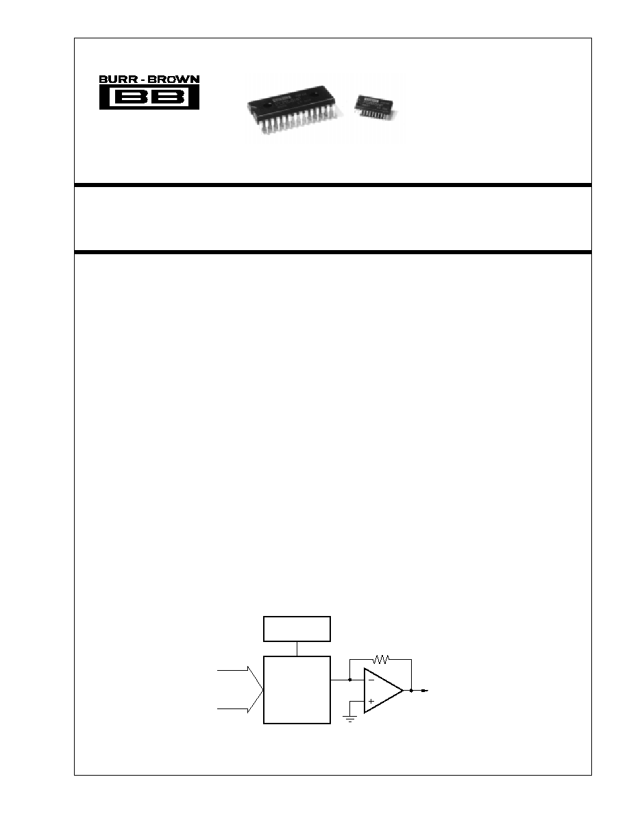
16-Bit Monolithic
DIGITAL-TO-ANALOG CONVERTERS
DESIGNED FOR AUDIO
DESCRIPTION
The PCM54 and PCM55 family of converters are
parallel input, fully monotonic, 16-bit digital-to-ana-
log converters that are designed and specified for
digital audio applications. These devices employ ul-
tra-stable nichrome (NiCr) thin-film resistors to pro-
vide monotonicity, low distortion, and low differential
linearity error (especially around bipolar zero) over
long periods of time and over the full operating
temperature.
These converters are completely self-contained with a
stable, low noise, internal, zener voltage reference;
high speed current switches; a resistor ladder
network; and a fast settling, low noise output opera-
tional amplifier all on a single monolithic chip. The
converters are operated using two power supplies that
can range from
±
5V (PCM55) to
±
12V (PCM54).
Power dissipation with
±
5V supplies is typically less
than 200mW. Also included is a provision for exter-
nal adjustment of the MSB error (differential linearity
error at bipolar zero, PCM54 only) to further improve
Total Harmonic Distortion (THD) specifications if
desired.
A current output (I
OUT
) wiring option is provided. This
output typically settles to within
±
0.006% of FSR
final value in 350ns (in response to a full-scale change
in the digital input code).
The PCM54 is packaged in 28-pin plastic DIP pack-
age. The PCM55 is available in a 24-lead plastic mini-
flatpak.
16-Bit Ladder
Resistor Network
and
Current Switches
Reference
Voltage
Parallel
Digital
Input
R
F
Output
Operational
Amplifier
Audio Output
(Voltage)
Æ
International Airport Industrial Park ∑ Mailing Address: PO Box 11400, Tucson, AZ 85734 ∑ Street Address: 6730 S. Tucson Blvd., Tucson, AZ 85706 ∑ Tel: (520) 746-1111 ∑ Twx: 910-952-1111
Internet: http://www.burr-brown.com/ ∑ FAXLine: (800) 548-6133 (US/Canada Only) ∑ Cable: BBRCORP ∑ Telex: 066-6491 ∑ FAX: (520) 889-1510 ∑ Immediate Product Info: (800) 548-6132
©
1985 Burr-Brown Corporation
PDS-619B
Printed in U.S.A. August, 1998
SBAS146

Æ
PCM54/55
2
SPECIFICATIONS
ELECTRICAL
At +25
∞
C and
±
V
CC
= 12V, unless otherwise noted.
V
Specifications same as for PCM54HP.
NOTES: (1) Externally adjustable. If external adjustment is not used, connect a 0.01
µ
F capacitor to Common to reduce noise pickup. (2) FSR means Full-Scale Range
and is 6V for
±
3V output. (3) The measurement of total harmonic distortion is highly dependent on the characteristics of the measurement circuit. Burr-Brown may
calculate THD from the measured linearity errors using Equation 2 in the section on "Total Harmonic Distortion," but specifies that the maximum THD measured with
the circuit shown in Figure 2 will be less than the limits indicated. (4) Measured with an active clamp to provide a low impedance for approximately 200ns. (5) Deglitcher
or sample/hold delay used in THD measurement test circuit. See Figures 2 and 3. (6) Output amplifier disconnected.
PCM54HP, PCM55HP
PCM54JP, PCM55JP
PCM54KP
PARAMETER
MIN
TYP
MAX
MIN
TYP
MAX
MIN
TYP
MAX
UNITS
DIGITAL INPUTS
Resolution
16
V
V
Bits
Dynamic Range
96
V
V
dB
Logic Levels (TTL/CMOS Compatible):
V
IH
+2.4
+5.25
V
V
V
V
V
V
IL
0
+0.8
V
V
V
V
V
I
IH
, V
IN
= +2.7V
+40
V
V
µ
A
I
IL
, V
IN
= +0.4V
≠0.5
V
V
mA
TRANSFER CHARACTERISTICS
ACCURACY
Gain Error
±
2
V
V
%
Bipolar Zero Error
±
30
V
V
mV
Differential Linearity Error at Biploar Zero
(1)
±
0.001
V
V
% FSR
(2)
Noise (rms) (20Hz to 20kHz) at Bipolar Zero
12
V
V
µ
V
TOTAL HARMONIC DISTORTION
(3)
(16-Bit Resolution)
V
O
=
±
FS at f = 991Hz
≠94
≠82
V
≠88
V
V
≠92
dB
V
O
= ≠20dB at f = 991Hz
≠74
≠68
V
V
V
≠80
≠74
dB
V
O
= ≠60dB at f = 991Hz
≠34
≠28
V
V
V
≠40
≠34
dB
MONOTONICITY
15
V
V
Bits
SETTLING TIME (to
±
0.006% of FSR)
Voltage Output: 6V Step
3
V
V
µ
s
1LSB Step
1
V
V
µ
s
Current Output (1mA Step): 10
to 100
Load
350
V
V
ns
1k
Load
(4)
350
V
V
ns
Deglitcher Delay (THD Test)
(5)
2.5
4
V
V
V
V
µ
s
Slew Rate
10
V
V
V/
µ
s
WARM-UP TIME
1
V
V
Min
ANALOG OUTPUT
Voltage Output: Bipolar Range
±
3
V
V
V
Output Current
±
2
V
V
mA
Output Impedance
0.1
V
V
Short-Circuit Duration
Indefinite to Common
V
V
Current Output:
(6)
Bipolar Range (
±
30%)
±
1
V
V
mA
Bipolar Output Impedance (
±
30%)
1.2
V
V
k
POWER SUPPLY REQUIREMENTS
Voltage: +V
CC
(PCM54)
+4.75
+12
+15.75
V
V
V
V
V
V
V
≠V
CC
(PCM54)
≠4.75
≠12
≠15.75
V
V
V
V
V
V
V
+V
CC
(PCM55)
+4.75
+5
+7.5
V
V
V
V
V
V
V
≠V
CC
(PCM55)
≠4.75
≠5
≠7.5
V
V
V
V
V
V
V
Supply Drain: +V
CC
+13
+20
V
V
V
V
mA
≠V
CC
≠16
≠25
V
V
V
V
mA
TEMPERATURE RANGE
Operating
0
+70
V
V
V
V
∞
C
Storage
≠55
+100
V
V
V
V
∞
C
The information provided herein is believed to be reliable; however, BURR-BROWN assumes no responsibility for inaccuracies or omissions. BURR-BROWN
assumes no responsibility for the use of this information, and all use of such information shall be entirely at the user's own risk. Prices and specifications are subject
to change without notice. No patent rights or licenses to any of the circuits described herein are implied or granted to any third party. BURR-BROWN does not
authorize or warrant any BURR-BROWN product for use in life support devices and/or systems.
Æ
PCM54/55
3
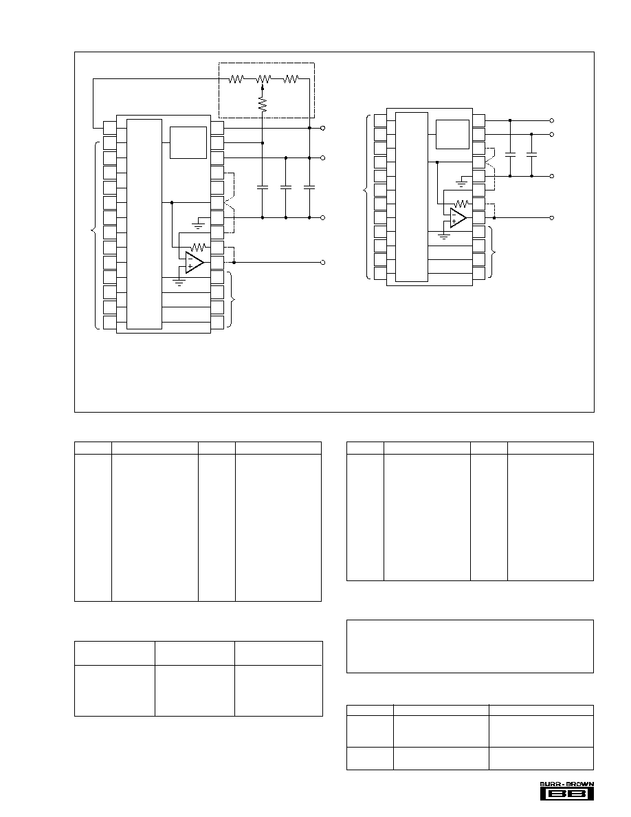
CONNECTION DIAGRAMS
PIN
PCM54-DIP
PIN
PCM54-DIP
1
Trim
15
Bit 13
2
Bit 1 (MSB)
16
Bit 14
3
Bit 2
17
Bit 15
4
NC
18
Bit 16 (LSB)
5
Bit 3
19
V
OUT
6
Bit 4
20
R
FB
7
Bit 5
21
SJ
8
Bit 6
22
Common
9
Bit 7
23
I
OUT
10
Bit 8
24
NC
11
Bit 9
25
I
BPO
12
Bit 10
26
+V
CC
13
Bit 11
27
MSB Adjust
14
Bit 12
28
≠V
CC
PIN ASSIGNMENTS
PIN
PCM55-SOIC
PIN
PCM55-SOIC
1
Bit 1 (MSB)
13
Bit 13
2
Bit 2
14
Bit 14
3
Bit 3
15
Bit 15
4
Bit 4
16
Bit 16
5
Bit 5
17
V
OUT
6
Bit 6
18
Feedback Resistor
7
Bit 7
19
Summing Junction
8
Bit 8
20
Common
9
Bit 9
21
Current Output
10
Bit 10
22
Bipolar Offset
11
Bit 11
23
+V
CC
12
Bit 12
24
≠V
CC
PIN ASSIGNMENTS
DC Supply Voltage ......................................................................
±
18VDC
Input Logic Voltage ............................................................... ≠1V to +5.5V
Power Dissipation .................................. PCM54 800mW, PCM55 400mW
Storage Temperature ...................................................... ≠55
∞
C to +100
∞
C
Lead Temperature, (soldering, 10s) .............................................. +300
∞
C
ABSOLUTE MAXIMUM RATINGS
ORDERING INFORMATION
PACKAGE INFORMATION
PACKAGE DRAWING
PRODUCT
PACKAGE
NUMBER
(1)
PCM54HP
28-Pin DIP
215
PCM54JP
28-Pin DIP
215
PCM54KP
28-Pin DIP
215
PCM55HP
24-Lead SOIC
178
PCM55JP
24-Lead SOIC
178
NOTE: (1) For detailed drawing and dimension table, please see end of data
sheet, or Appendix C of Burr-Brown IC Data Book.
PRODUCT
THD at FS
PACKAGE
PCM54HP
0.008
28-Pin DIP
PCM54JP
0.004
28-Pin DIP
PCM54KP
0.0025
28-Pin DIP
PCM55HP
0.008
24-Lead SOIC
PCM55JP
0.004
24-Lead SOIC
1
2
3
4
5
6
7
8
9
10
11
12
13
14
28
27
26
25
24
23
22
21
20
19
18
17
16
15
0.1
µ
F
PCM54
16-Bit
Ladder
Resistor
Network
and
Switches
Zener
Voltage
Reference
Data
Inputs
1
µ
F
1
µ
F
(2)
(3)
+
+
Common
+V
CC
Audio
V
OUT
100k
560k
330k
1M
(1)
≠V
CC
(Optional)
Data Inputs
24
23
22
21
20
19
18
17
16
15
14
13
1µF
PCM55
16-Bit
Ladder
Resistor
Network
and
Switches
Zener
Voltage
Reference
Data
Inputs
1µF
(2)
+
Common
+V
CC
Audio
V
OUT
(1)
≠V
CC
Data Inputs
1
2
3
4
5
6
7
8
9
10
11
12
+
(2)
NOTES: (1) MSB error (BPZ differential linearity error) can be adjusted to zero
using this external circuit. (2) Connect to bipolar operation (+V
CC
8.5V for
unipolar operation). (3) Connect for V
OUT
operation. When V
OUT
amp is not being
used (I
OUT
mode), terminate with an external 3k
feedback resistor between pin
19 and pin 21, and a 1k
resistor between pin 21 and pin 22 to reduce possible
noise effects.
NOTES: (1) Connect for bipolar operation. (+V
CC
8.5V for unipolar operation.)
(2) Connect for V
OUT
operation. When V
OUT
amp is not being used (I
OUT
mode),
terminate with an external 3k
feedback resistor between pin 17 and pin 19, and
a 1k
resistor between pin 19 and pin 20 to reduce possible noise effects.

Æ
PCM54/55
4
DISCUSSION OF
SPECIFICATIONS
The PCM54 and PCM55 are specified to provide critical
performance criteria for a wide variety of applications. The
most critical specifications for a D/A converter in audio
applications are total harmonic distortion, differential linear-
ity error, bipolar zero error, parameter shifts with time and
temperature, and settling time effects on accuracy.
The PCM54 and PCM55 are factory-trimmed and tested for
all critical key specifications.
The accuracy of a D/A converter is described by the transfer
function shown in Figure 1. Digital input to analog output
relationship is shown in Table I. The errors in the D/A
converter are combinations of analog errors due to the linear
circuitry, matching and tracking properties of the ladder and
scaling networks, power supply rejection, and reference
errors. In summary, these errors consist of initial errors
including gain, offset, linearity, differential linearity, and
power supply sensitivity. Gain drift over temperature rotates
the line (Figure 1) about the bipolar zero point and offset
drift shifts the line left or right over the operating tempera-
ture range. Most of the offset and gain drift with temperature
or time is due to the drift of the internal reference zener
diode. The converter is designed so that these drifts are in
opposite directions. This way, the bipolar zero voltage is
virtually unaffected by variations in the reference voltage.
DIGITAL INPUT CODES
The PCM54 and PCM55 accept complementary digital
input codes in any of three binary formats (CSB, unipolar; or
COB, bipolar; or CTC, Complementary Two's Comple-
ment, bipolar). See Table II.
Gain
Drift
Offset
Drift
Bipolar
Zero
≠FSR/2
(+FSR/2) ≠1LSB
Digital Input
Analog Output
0000...0000
0000...0001
0111...1101
0111...1110
0111...1111
1000...0000
1000...0001
1111...1110
1111...1111
All Bits
On
* See Table I for digital code definitions.
FIGURE 1. Input vs Output for an Ideal Bipolar D/A
Converter.
ANALOG OUTPUT
Digital
Complementary
Complementary
Complementary
Input
Straight Binary
Offset Binary
Two's Complement
Codes
(CSB)
(COB)
(CTS)
(1)
0000
H
+Full Scale
+Full Scale
≠1LSB
7FFF
H
+1/2 Full Scale
Bipolar Zero
≠Full Scale
8000
H
+1/2 Full Scale
≠1LSB
+Full Scale
≠1LSB
FFFF
H
Zero
≠Full Scale
Bipolar Zero
NOTE: (1) Invert the MSB of the COB code with an external inverter to obtain
CTC code.
TABLE II. Digital Input Codes.
BIPOLAR ZERO ERROR
Initial Bipolar Zero (BPZ) error (Bit 1 "ON" and all other
bits "OFF") is the deviation from 0V out and is factory-
trimmed to typically
±
10mV at +25
∞
C.
DIFFERENTIAL LINEARITY ERROR
Differential Linearity Error (DLE) is the deviation from an
ideal 1LSB change from one adjacent output state to the
next. DLE is important in audio applications because exces-
sive DLE at bipolar zero (at the "major carry") can result in
audible crossover distortion for low level output signals.
Initial DLE on the PCM54 and PCM55 is factory-trimmed
to typically
±
0.001% of FSR. This error is adjustable to zero
using the circuit shown in the connection diagram (PCM54
only).
VOLTAGE OUTPUT MODE
Analog Output
Unipolar
(1)
Bipolar
Digital Input Code
16-Bit
15-Bit
14-Bit
16-Bit
15-Bit
14-Bit
One LSB
(
µ
V)
91.6
183
366
91.6
183
366
0000
H
(V)
+5.99991
+5.99982
+5.99963
+2.99991
+2.99982
+2.99963
FFFF
H
(V)
0
0
0
≠3.0000
≠3.0000
≠3.0000
CURRENT OUTPUT MODE
Analog Output
Unipolar
Bipolar
Digital Input Code
16-Bit
15-Bit
14-Bit
16-Bit
15-Bit
14-Bit
One LSB
(
µ
A)
0.031
0.061
0.122
0.031
0.061
0.122
0000
H
(mA)
≠1.99997
≠1.99994
≠1.99988
≠0.99997
≠0.99994
≠0.99988
FFFF
H
(mA)
0
0
0
+1.00000
+1.00000
+1.00000
NOTE: (1) +V
CC
must be at least +8.5VDC to allow output to swing to +6.0VDC.
TABLE I. Digital Input to Analog Output Relationship.
Æ
PCM54/55
5
POWER SUPPLY SENSITIVITY
Changes in the DC power supplies will affect accuracy.
The PCM54 and PCM55 power supply sensitivity is shown
by Figure 2. Normally, regulated power supplies with 1% or
less ripple are recommended for use with the DAC. See also
Power Supply Connections paragraph in the Installation and
Operating Instructions section.
SETTLING TIME
Settling time is the total time (including slew time) required
for the output to settle within an error band around its final
value after a change in input (see Figure 3).
Settling times are specified to
±
0.006% of FSR; one for a
large output voltage change of 3V and one for a 1LSB
change. The 1LSB change is measured at the major carry
(0111...11 to 10000.00), the point at which the worst-case
settling time occurs.
STABILITY WITH TIME AND TEMPERATURE
The parameters of a D/A converter designed for audio
applications should be stable over a relatively wide tempera-
ture range and over long periods of time to avoid undesirable
periodic readjustment. The most important parameters are
bipolar zero, differential linearity error, and total harmonic
distortion. Most of the offset and gain drift with temperature
or time is due to the drift of the internal reference zener
diode. The PCM54 and PCM55 are designed so that these
drifts are in opposite directions so that the bipolar zero
voltage is virtually unaffected by variations in the reference
voltage. Both DLE and THD are dependent upon the match-
ing and tracking of resistor ratios and upon V
BE
and h
FE
of
the current-source transistors. The PCM54 and PCM55 were
designed so that any absolute shift in these components has
virtually no effect on DLE or THD. The resistors are made
of identical links of ultra-stable nichrome thin-film. The
current density in these resistors is very low to further
enhance their stability.
DYNAMIC RANGE
The dynamic range is a measure of the ratio of the smallest
signals the converter can produce to the full-scale range and
is usually expressed in decibels (dB). The theoretical dy-
namic range of a converter is approximately 6 x n, or about
96dB for a 16-bit converter. The actual, or useful, dynamic
range is limited by noise and linearity errors and is therefore
somewhat less than the theoretical limit. However, this does
point out that a resolution of at least 16 bits is required to
obtain a 90dB minimum dynamic range, regardless of the
accuracy of the converter. Another specification that is
useful for audio applications is total harmonic distortion.
TOTAL HARMONIC DISTORTION
THD is useful in audio applications and is a measure of the
magnitude and distribution of the linearity error, differential
linearity error, and noise as well as quantization error. To be
useful, THD should be specified for both high level and low
level input signals. This error is unadjustable and is the most
meaningful indicator of D/A converter accuracy for audio
applications.
The THD is defined as the ratio of the square root of the sum
of the squares of the values of the harmonics to the value of
the fundamental input frequency and is expressed in percent
or dB. The rms value of the PCM54/55 error referred to the
input can be shown to be:
(1)
where n is the number of samples in one cycle of any given
sine wave, E
L
(i) is the linearity error of the PCM54 or
PCM55 at each sampling point, and E
Q
(i) is the quantization
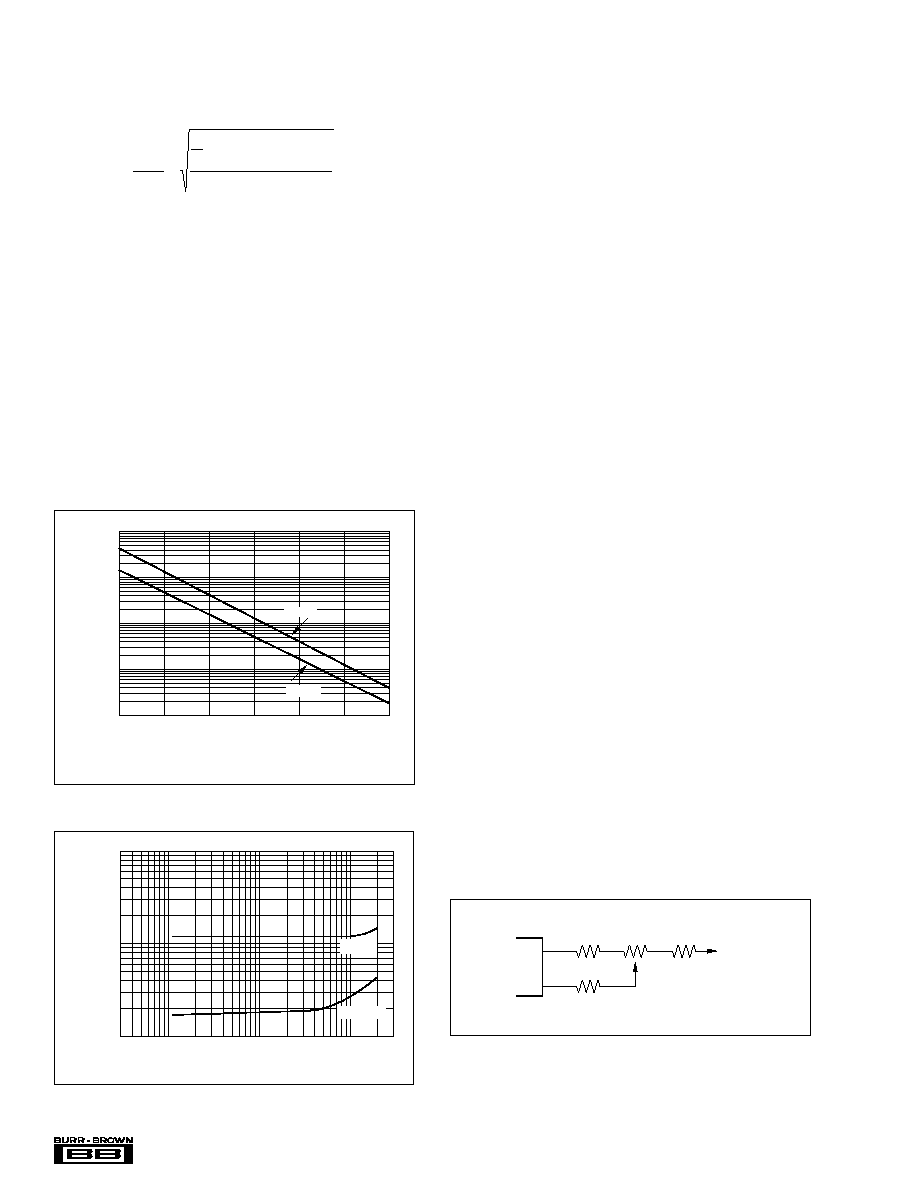
10.0
3.0
1.0
0.30
0.10
0.03
0.01
0.003
0.001
5
10
15
±
V
CC
Supplies (V)
THD (%)
0dB
≠60dB
≠20dB
FIGURE 2. Effects of
±
V
CC
on Total Harmonic Distortion
(PCM54JP; V
CC
s with approximately 2% ripple).
rms
i
n
L
Q
n
i
i
=
+
=
1
1
2
[
( )
( )]
FIGURE 3. Full-Scale Range Settling Time vs Accuracy.
1.0
0.3
0.1
0.03
0.01
0.003
0.001
0.01
0.1
1.0
10.0
Settling Time (
µ
s)
Accuracy Percent Full-Scale Range (%)
R
L
= 200
Current
Output
Mode
Voltage
Output
Mode
Æ
PCM54/55
6
error at each sampling point. The THD can then be ex-
pressed as:
(2)
where E
rms
is the rms signal voltage level.
This expression indicates that, in general, there is a correla-
tion between the THD and the square root of the sum of the
squares of the linearity errors at each digital word of interest.
However, this expression does not mean that the worst-case
linearity error of the D/A is directly correlated to the THD.
For PCM54/55 the test period was chosen to be 22.7
µ
s
(44.1kHz) which is compatible with the EIAJ STC-007
specification for PCM audio. The test frequency is 420Hz
and the amplitude of the input signal is 0dB, ≠20dB, and
≠60dB down from full scale.
Figure 4 shows the typical THD as a function of output
voltage.
Figure 5 shows typical THD as a function of frequency.
THD
n
i
i
rms
rms
i
n
L
Q
rms
=
=
+
=
1
100
1
2
[
( )
( )]
∑
%
INSTALLATION AND OPERATING
INSTRUCTIONS
POWER SUPPLY CONNECTIONS
For optimum performance and noise rejection, power supply
decoupling capacitors should be added as shown in the
connections diagram. These capacitors (1
µ
F tantalum or
electrolytic recommended) should be located close to the
converter.
MSB ERROR ADJUSTMENT PROCEDURE
(OPTIONAL)
The MSB error of the PCM54 and PCM55 can be adjusted
to make the differential linearity error (DLE) at BPZ essen-
tially zero. This is important when the signal output levels
are very low because zero crossing noise (DLE at BPZ)
becomes very significant when compared to the small code
changes occurring in the LSB portion of the converter.
Differential linearity error at bipolar zero is guaranteed to
meet data sheet specifications without any external adjust-
ment. However, a provision has been made for an optional
adjustment of the MSB linearity point which makes it
possible to eliminate DLE error at BPZ (PCM54 only). Two
procedures are given to allow either static or dynamic
adjustment. The dynamic procedure is preferred because of
the difficulty associated with the static method (accurately
measuring 16-bit LSB steps).
To statically adjust DLE at BPZ, refer to the circuit shown
in Figure 6 or the PCM54 connection diagram. After allow-
ing ample warm-up time (20-30 minutes) to assure stable
operation of the PCM54, select input code 8000 hexadeci-
mal (all bits off except the MSB). Measure and record it.
Change the digital input code to 7FFF hexadecimal (all bits
off except the MSB). Adjust the 100k
potentiometer to
make the audio output read 92
µ
V more than the voltage
reading of the previous code (a ILSB step = 92
µ
V).
A much simpler method is to dynamically adjust the DLE at
BPZ. Again, refer to Figure 6 or the PCM54 connection
diagram for circuitry and component values. Assuming the
device has been installed in a digital audio application
circuit, send the appropriate digital input to produce a ≠60dB
level sinusoidal output. While measuring the THD of the
audio circuit output, adjust the 100k
potentiometer until a
minimum level of distortion is observed.
0.1
0.05
0.02
0.01
0.005
0.002
0.001
100
1k
10k 20k
Frequency (Hz)
Total Harmonic Distortion (%)
≠20dB
Full Scale
FIGURE 5. Total Harmonic Distortion (THD) vs
Frequency.
10.0
4.0
2.0
1.0
0.4
0.2
0.1
0.04
0.02
0.01
0.004
0.002
0.001
≠60
≠50
≠40
≠30
≠20
≠10
0
V
OUT
(dB)
T
otal Har
monic Distor
tion (THD) in %
0dB = Full-Scale Range (FSR)
16 Bits
14 Bits
FIGURE 4. Total Harmonic Distortion (THD) vs V
OUT
.
FIGURE 6. MSB Differential Linearity at Bipolar Zero Ad-
justment Circuit (optional).
1M
560k
100k
330k
≠V
CC
1
27
Æ
PCM54/55
7
Due to the fast settling time of the PCM54-V, it is possible
to minimize the delay between the left channel and right
channel outputs when using a single D/A converter for both
channels. This is important because the left and right chan-
nel data is recorded in phase and use of a slower D/A
converter would result in significant phase error at the
higher audio frequencies.
A low-pass filter is required at the S/H output to remove all
unwanted frequency components caused by the sampling
frequency as well as the discrete nature of the D/A converter
output. The filter must have a flat amplitude response over
the entire audio band (0 to 20kHz) and a very high attenu-
ation above 20kHz. Most previous digital audio circuits used
a high-order (9-13 pole) analog filter. However, the phase
response of an analog filter with these amplitude character-
istics is nonlinear and can disturb the pulse-shaped charac-
teristics of the transients contained in music.
INSTALLATION
CONSIDERATIONS
If the optional external MSB error circuitry is used (PCM54),
a potentiometer with adequate resolution and a TCR of
100ppm/
∞
C or less is required. Also, extra care must be
taken to insure that no leakage path (either AC or DC) exists
to pin 27 (PCM54). If circuit is not used, pin 1 (PCM54)
should be terminated to common with a 0.01
µ
F capacitor.
The PCM converter and the wiring to its connectors should
be located to provide the optimum isolation from sources of
RFI and EMI. The important consideration in the elimina-
tion of RF radiation or pickup is loop area; therefore, signal
leads and their return conductors should be kept close
together. This reduces the external magnetic field along with
any radiation. Also, if a signal lead and its return conductor
are wired close together, they represent a small flux-capture
cross section for any external field. This reduces radiation
pickup in the circuit.
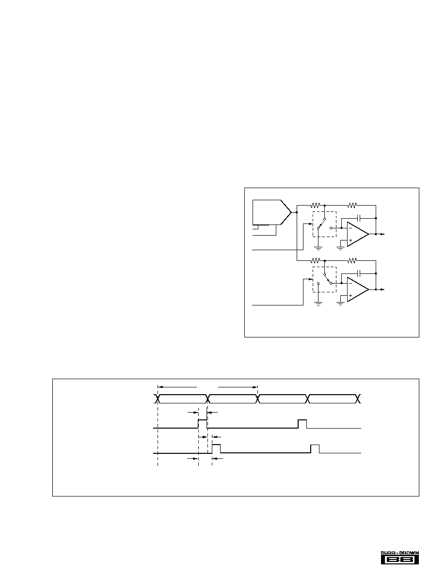
APPLICATIONS
A sample/hold amplifier, or "deglitcher", is required at the
output of the D/A converter for both the left and right
channel, as shown in Figure 7. The S/H amplifier for the left
channel is composed of A
2
, SW
1
, and associated circuitry. A
2
is used as an integrator to hold the analog voltage in C
1
.
Since the source and drain of the FET switch operates at a
virtual ground when "C" and "B" are closed in the simple
mode, there is no increase in distortion caused by the
modulation effect of R
ON
by the audio signal.
Figure 8 shows the deglitcher control signals for both the left
and right channels which are produced by the timing control
logic. A delay of 2.5
µ
s (t
) is provided to eliminate the
glitch and allow the output of the PCM54-V to settle within
a small error band around its final value before connecting
it to the channel output.
PCM54/55
A
1
C
1
C
A
B
SW
1
Left Channel Output to LPF
and Other Circuits
Left Channel
Deglitcher Control
R
R
R
R
A
2
C
2
C
A
B
SW
2
Right Channel Output to LPF
and Other Circuits
A
1
, A
2
ATE
OPA101 or OPA404
Right Channel
Deglitcher Control
Data to
DAC
A LOW signal on the
deglitcher control closes switch "A",
while a HIGH signal closes switch "B".
FIGURE 7. A Sample/Hold Amplifier (deglitcher) is Re-
quired at the Digital-to-Analog Output for Both
Left and Right Channels.
Right Channel Data N
Left Channel Data N
Right Channel Data N+1
Left Channel Data N+1
44.1kHz
Delay Between Left and Right Channel
Data for DAC
Right Channel
Deglitcher Control
Left Channel
Deglitcher Control
The deglitcher control signals are generated by the timing control logic. The fast settling time of the
PCM54/55 makes it possible to minimize the delay between left and right channels to approximately 4.5
µ
s
which reduces phase error at the higher audio frequencies.
t
S
t
W
FIGURE 8. Timing Diagram for the Deglitcher Control Signals.

PACKAGING INFORMATION
ORDERABLE DEVICE
STATUS(1)
PACKAGE TYPE
PACKAGE DRAWING
PINS
PACKAGE QTY
PCM54HP
ACTIVE
PDIP
NTD
28
12
PCM54JP
ACTIVE
PDIP
NTD
28
12
PCM54KP
ACTIVE
PDIP
NTD
28
12
PCM55HP
ACTIVE
SOP
DVK
24
30
PCM55HP/1K
ACTIVE
SOP
DVK
24
1000
PCM55JP
ACTIVE
SOP
DVK
24
30
(1) The marketing status values are defined as follows:
ACTIVE: Product device recommended for new designs.
LIFEBUY: TI has announced that the device will be discontinued, and a lifetime-buy period is in effect.
NRND: Not recommended for new designs. Device is in production to support existing customers, but TI does not recommend using this part in
a new design.
PREVIEW: Device has been announced but is not in production. Samples may or may not be available.
OBSOLETE: TI has discontinued the production of the device.
PACKAGE OPTION ADDENDUM
www.ti.com
3-Oct-2003

IMPORTANT NOTICE
Texas Instruments Incorporated and its subsidiaries (TI) reserve the right to make corrections, modifications,
enhancements, improvements, and other changes to its products and services at any time and to discontinue
any product or service without notice. Customers should obtain the latest relevant information before placing
orders and should verify that such information is current and complete. All products are sold subject to TI's terms
and conditions of sale supplied at the time of order acknowledgment.
TI warrants performance of its hardware products to the specifications applicable at the time of sale in
accordance with TI's standard warranty. Testing and other quality control techniques are used to the extent TI
deems necessary to support this warranty. Except where mandated by government requirements, testing of all
parameters of each product is not necessarily performed.
TI assumes no liability for applications assistance or customer product design. Customers are responsible for
their products and applications using TI components. To minimize the risks associated with customer products
and applications, customers should provide adequate design and operating safeguards.
TI does not warrant or represent that any license, either express or implied, is granted under any TI patent right,
copyright, mask work right, or other TI intellectual property right relating to any combination, machine, or process
in which TI products or services are used. Information published by TI regarding third-party products or services
does not constitute a license from TI to use such products or services or a warranty or endorsement thereof.
Use of such information may require a license from a third party under the patents or other intellectual property
of the third party, or a license from TI under the patents or other intellectual property of TI.
Reproduction of information in TI data books or data sheets is permissible only if reproduction is without
alteration and is accompanied by all associated warranties, conditions, limitations, and notices. Reproduction
of this information with alteration is an unfair and deceptive business practice. TI is not responsible or liable for
such altered documentation.
Resale of TI products or services with statements different from or beyond the parameters stated by TI for that
product or service voids all express and any implied warranties for the associated TI product or service and
is an unfair and deceptive business practice. TI is not responsible or liable for any such statements.
Following are URLs where you can obtain information on other Texas Instruments products and application
solutions:
Products
Applications
Amplifiers
amplifier.ti.com
Audio
www.ti.com/audio
Data Converters
dataconverter.ti.com
Automotive
www.ti.com/automotive
DSP
dsp.ti.com
Broadband
www.ti.com/broadband
Interface
interface.ti.com
Digital Control
www.ti.com/digitalcontrol
Logic
logic.ti.com
Military
www.ti.com/military
Power Mgmt
power.ti.com
Optical Networking
www.ti.com/opticalnetwork
Microcontrollers
microcontroller.ti.com
Security
www.ti.com/security
Telephony
www.ti.com/telephony
Video & Imaging
www.ti.com/video
Wireless
www.ti.com/wireless
Mailing Address:
Texas Instruments
Post Office Box 655303 Dallas, Texas 75265
Copyright
2003, Texas Instruments Incorporated