 | ÐлекÑÑоннÑй компоненÑ: PGA2311PA | СкаÑаÑÑ:  PDF PDF  ZIP ZIP |
Äîêóìåíòàöèÿ è îïèñàíèÿ www.docs.chipfind.ru
SBOS218A DECEMBER 2001 REVISED JUNE 2002
Stereo Audio Volume Control
PGA2311
FEATURES
D
DIGITALLY-CONTROLLED ANALOG VOLUME
CONTROL
Two Independent Audio Channels
Serial Control Interface
Zero Crossing Detection
Mute Function
D
WIDE GAIN AND ATTENUATION RANGE
+31.5dB to 95.5dB with 0.5dB Steps
D
LOW NOISE AND DISTORTION
120dB Dynamic Range
0.0004% THD+N at 1kHz (U-Grade)
0.0002% THD+N at 1kHz (A-Grade)
D
NOISE-FREE LEVEL TRANSITIONS
D
LOW INTERCHANNEL CROSSTALK
130dBFS
D
POWER SUPPLIES:
±
5V Analog, +5V Digital
D
AVAILABLE IN DIP-16 AND SOL-16
PACKAGES
D
PIN AND SOFTWARE COMPATIBLE WITH THE
CRYSTAL CS3310
APPLICATIONS
D
AUDIO AMPLIFIERS
D
MIXING CONSOLES
D
MULTI-TRACK RECORDERS
D
BROADCAST STUDIO EQUIPMENT
D
MUSICAL INSTRUMENTS
D
EFFECTS PROCESSORS
D
A/V RECEIVERS
D
CAR AUDIO SYSTEMS
DESCRIPTION
The PGA2311 is a highperformance, stereo audio
volume control designed for professional and high-end
consumer audio systems. Using high performance
operational amplifier stages internal to the PGA2311
yields low noise and distortion, while providing the
capability to drive 600
loads directly without buffering.
The 3-wire serial control interface allows for connection
to a wide variety of host controllers, in addition to
support for daisy-chaining of multiple PGA2311
devices.
www.ti.com
Please be aware that an important notice concerning availability, standard warranty, and use in critical applications of Texas Instruments
semiconductor products and disclaimers thereto appears at the end of this data sheet.
Copyright
2001, Texas Instruments Incorporated
PRODUCTION DATA information is current as of publication date. Products
conform to specifications per the terms of Texas Instruments standard warranty.
Production processing does not necessarily include testing of all parameters.
Please be aware that an important notice concerning availability, standard warranty, and use in critical applications of Texas Instruments
semiconductor products and disclaimers thereto appears at the end of this data sheet.
PGA2311
SBOS218A DECEMBER 2001 REVISED JUNE 2002
www.ti.com
2
ABSOLUTE MAXIMUM RATINGS
(1)
Supply Voltage, VA+
+5.5V
. . . . . . . . . . . . . . . . . . . . . . . . . . . .
VA
5.5V
. . . . . . . . . . . . . . . . . . . . . . . . . . . . . . . . . . . . . .
VD+
+5.5V
. . . . . . . . . . . . . . . . . . . . . . . . . . . . . . . . . . . . . .
VA+ to VD+
<
±
0.3V
. . . . . . . . . . . . . . . . . . . . . . . . . . . . . . . . .
Analog Input Voltage
0V to VA+, VA
. . . . . . . . . . . . . . . . . . . . . .
Digital Input Voltage
0.3V to VD+
. . . . . . . . . . . . . . . . . . . . . . . . .
Operating Temperature Range
40
°
C to +85
°
C
. . . . . . . . . . . . . . . .
Storage Temperature Range
65
°
C to +150
°
C
. . . . . . . . . . . . . . . .
Junction Temperature
+150
°
C
. . . . . . . . . . . . . . . . . . . . . . . . . . .
Lead Temperature (soldering, 10s)
+300
°
C
. . . . . . . . . . . . . . . . . . .
Package Temperature (IR reflow, 10s)
+235
°
C
. . . . . . . . . . . . . . . . .
(1) Stresses above these ratings may cause permanent damage.
Exposure to absolute maximum conditions for extended periods
may degrade device reliability.
ELECTROSTATIC
DISCHARGE SENSITIVITY
This integrated circuit can be damaged by ESD. Texas
Instruments recommends that all integrated circuits be
handled with appropriate precautions. Failure to ob-
serve proper handling and installation procedures can
cause damage.
ESD damage can range from subtle performance
degradation to complete device failure. Precision
integrated circuits may be more susceptible to damage
because very small parametric changes could cause
the device not to meet its published specifications.
PACKAGE/ORDERING INFORMATION
PRODUCT
PACKAGELEAD
PACKAGE
DESIGNATOR(1)
OPERATING
TEMPERATURE
RANGE
PACKAGE
MARKING
ORDERING
NUMBER
TRANSPORT
MEDIA, QUANTITY
DIP16
N
PGA2311P
PGA2311P
Rails
PGA2311 (UGrade)
SOL 16
DW
40
°
C to +85
°
C
PGA2311U
PGA2311U
Rails
PGA2311 (U Grade)
SOL16
DW
40 C to +85 C
PGA2311U
PGA2311U/1K
Tape and Reel, 1000
DIP16
N
PGA2311PA
PGA2311PA
Rails
PGA2311 (AGrade)
SOL 16
DW
40
°
C to +85
°
C
PGA2311UA
PGA2311UA
Rails
PGA2311 (A Grade)
SOL16
DW
40 C to +85 C
PGA2311UA
PGA2311UA/1K
Tape and Reel, 1000
(1) For the most current specifications and package information, refer to our web site at www. ti.com.
ELECTRICAL CHARACTERISTICS
At TA = +25
°
C, VA+ = +5V, VA = 5V, VD+ = +5V, RL = 100k
, CL = 20pF, BW measure = 10Hz to 20kHz, unless otherwise noted.
PARAMETER
CONDITIONS
PGA2311P, U (UGrade).
PGA2311PA, UA (AGrade)
UNITS
PARAMETER
CONDITIONS
MIN
TYP
MAX
MIN
TYP
MAX
UNITS
DC CHARACTERISTICS
Step Size
0.5
0.5
dB
Gain Error
Gain Setting = 31.5dB
±
0.05
±
0.05
dB
Gain Matching
±
0.05
±
0.05
dB
Input Resistance
10
10
k
Input Capacitance
3
3
pF
AC CHARACTERISTICS
THD+N
VIN = 2Vrms, f = 1kHz
0.0004
0.001
0.0002
0.0004
%
Dynamic Range
VIN = AGND, Gain = 0dB
116
120
116
120
dB
Voltage Range, Output
(VA) +
1.25
(VA+)
1.25
(VA) +
1.25
(VA+)
1.25
V
Voltage Range, Input (without clipping)
2.5
2.5
Vrms
Output Noise
VIN = AGND, Gain = 0dB
2.5
4
2.5
4
µ
Vrms
Interchannel Crosstalk
f = 1kHz
130
130
dBFS
OUTPUT BUFFER
Offset Voltage
VIN = AGND, Gain = 0dB
0.25
0.5
0.25
0.5
mV
Load Capacitance Stability
100
100
pF
ShortCircuit Current
50
50
mA
UnityGain Bandwidth, Small Signal
10
10
MHz
PGA2311
SBOS218A DECEMBER 2001 REVISED JUNE 2002
www.ti.com
3
ELECTRICAL CHARACTERISTICS
(Cont.)
At TA = +25
°
C, VA+ = +5V, VA = 5V, VD+ = +5V, RL = 100k
, CL = 20pF, BW measure = 10Hz to 20kHz, unless otherwise noted.
PARAMETER
CONDITIONS
PGA2311P, U (UGrade)
PGA2311PA, UA (AGrade)
UNITS
PARAMETER
CONDITIONS
MIN
TYP
MAX
MIN
TYP
MAX
UNITS
DIGITAL CHARACTERISTICS
HighLevel Input Voltage, VIH
+2.0
VD+
+2.0
VD+
V
LowLevel Input Voltage, VIL
0.3
0.8
0.3
0.8
V
HighLevel Output Voltage, VOH
IO = 200
µ
A
(VA+)
1.0
(VD+)
1.0
V
LowLevel Output Voltage, VOL
IO = 3.2mA
0.4
0.4
V
Input Leakage Current
1
10
1
10
µ
A
SWITCHING CHARACTERISTICS
Serial Clock (SCLK) Frequency
fSCLK
0
6.25
0
6.25
MHz
Serial Clock (SCLK) Pulse Width LOW
tPH
80
80
ns
Serial Clock (SCLK) Pulse Width HIGH
tPL
80
80
ns
MUTE Pulse Width LOW
tMI
2.0
2.0
ms
Input Timing
SDI Setup Time
tSDS
20
20
ns
SDI Hold Time
tSDH
20
20
ns
CS Falling to SCLK Rising
tCSCR
90
90
ns
SCLK Falling to CS Rising
tCFCS
35
35
ns
Output Timing
CS LOW to SDO Active
tCSO
35
35
ns
SCLK Falling to SDO Data Valid
tCFDO
60
60
ns
CS HIGH to SDO High Impedance
tCSZ
100
100
ns
POWER SUPPLY
Operating Voltage
VA+
+4.75
+5
+5.25
+4.75
+5
+5.25
V
VA
4.75
5
5.25
4.75
5
5.25
V
VD+
+4.75
+5
+5.25
+4.75
+5
+5.25
V
Quiescent Current
IA+
VA+ = +5V
8
10
8
10
mA
IA
VA = 5V
10
12
10
12
mA
ID+
VD+ = +5V
0.5
1.0
0.5
1.0
mA
PowerSupply Rejection Ratio PSRR (250Hz)
100
100
dB
TEMPERATURE RANGE
Operating Range
40
+85
40
+85
°
C
Storage Range
65
+150
65
+150
°
C
Thermal Resistance, JC
DIP16
60
60
°
C/W
SOL16
50
50
°
C/W
PGA2311
SBOS218A DECEMBER 2001 REVISED JUNE 2002
www.ti.com
4
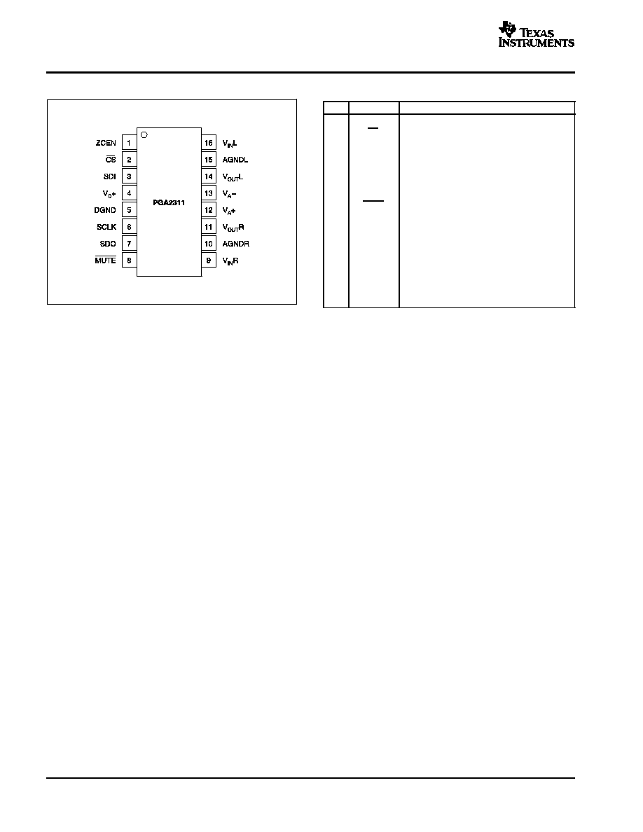
PIN CONFIGURATION
Top View
DIP, SOL
PIN ASSIGNMENTS
PIN
NAME
FUNCTION
1
ZCEN
Zero Crossing Enable Input (Active HIGH)
2
CS
Chip Select Input (Active LOW)
3
SDI
Serial Data input
4
VD+
Digital Power Supply, +5V
5
DGND
Digital Ground
6
SCLK
Serial Clock Input
7
SDO
Serial Data Output
8
MUTE
Mute Control Input (Active LOW)
9
VINR
Analog Input, Right Channel
10
AGNDR
Analog Ground, Right Channel
11
VOUTR
Analog Output, Right Channel
12
VA+
Analog Power Supply, +5V
13
VA
Analog Power Supply, 5V
14
VOUTL
Analog Output, Left Channel
15
AGNDL
Analog Ground, Left Channel
16
VINL
Analog Input, Left Channel
PGA2311
SBOS218A DECEMBER 2001 REVISED JUNE 2002
www.ti.com
5
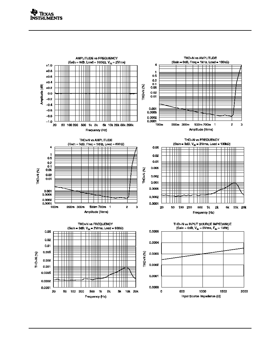
TYPICAL CHARACTERISTICS
At TA = +25
°
C, VA+ = +5V, VA = 5V, VD+ = +5V, RL = 100k
, CL = 20pF, BW measure = 10Hz to 20kHz, unless otherwise noted.
(NOTE: All plots taken with PGA2311 AGrade.)
PGA2311
SBOS218A DECEMBER 2001 REVISED JUNE 2002
www.ti.com
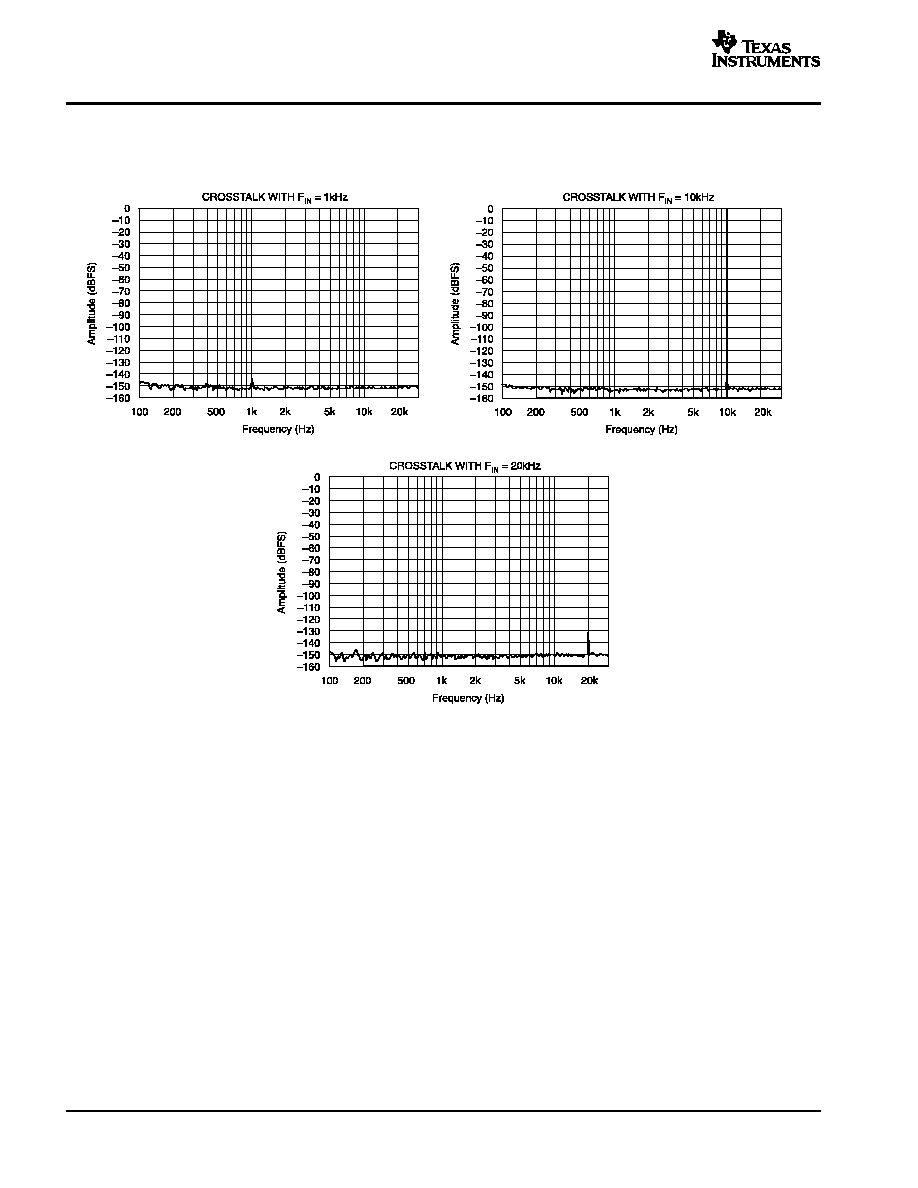
6
TYPICAL CHARACTERISTICS (CONT.)
At TA = +25
°
C, VA+ = +5V, VA = 5V, VD+ = +5V, RL = 100k
, CL = 20pF, BW measure = 10Hz to 20kHz, unless otherwise noted.
(NOTE: All plots taken with PGA2311 AGrade.)
PGA2311
SBOS218A DECEMBER 2001 REVISED JUNE 2002
www.ti.com
7
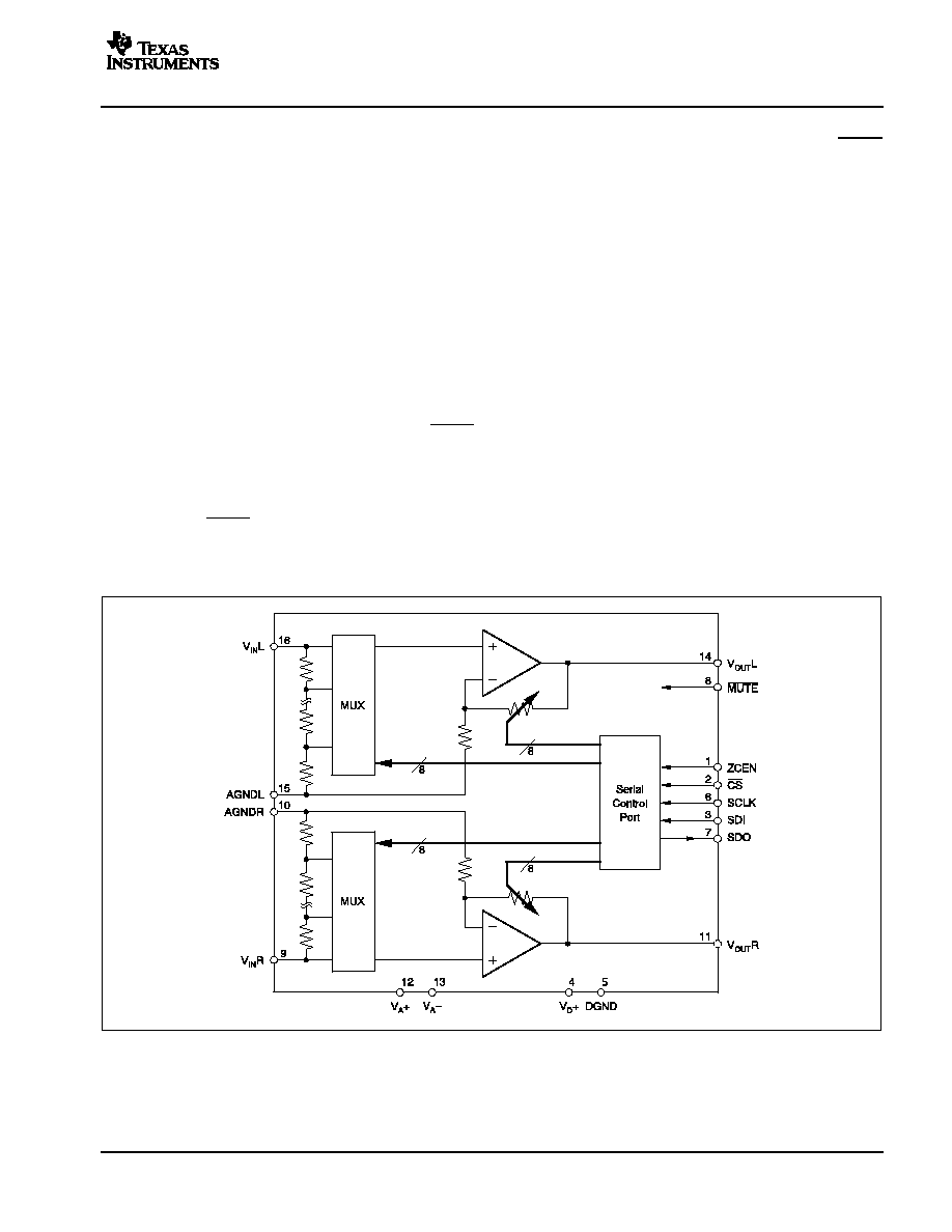
GENERAL DESCRIPTION
The PGA2311 is a stereo audio volume control. It may
be used in a wide array of professional and consumer
audio equipment. The PGA2311 is fabricated in a sub
micron CMOS process.
The heart of the PGA2311 is a resistor network, an ana-
log switch array, and a highperformance op amp
stage. The switches are used to select taps in the resis-
tor network that, in turn, determine the gain of the am-
plifier stage. Switch selections are programmed using
a serial control port. The serial port allows connection
to a wide variety of host controllers. Figure 1 shows a
functional block diagram of the PGA2311.
POWERUP STATE
On power up, "powerup reset" is activated for about
100ms during which the circuit is in hardware MUTE
state and all internal flip-flops are reset. At the end of this
period, the offset calibration is initiated without any exter-
nal signals. Once this has been completed, the gain byte
value for both the left and right channels are set to 00
HEX
,
or the software MUTE condition. The gain will remain at
this setting until the host controller programs new set-
tings for for each channel via the serial control port.
If during normal operation the power supply voltage
drops below
±
3.2V, the circuit enters a hardware MUTE
state. A power-up sequence will be initiated if the power
supply voltage returns to greater than
±
3.2V.
ANALOG INPUTS AND OUTPUTS
The PGA2311 includes two independent channels, re-
ferred to as the left and right channels. Each channel has
a corresponding input and output pin. The input and out-
put pins are unbalanced, or referenced to analog ground
(either AGNDR or AGNDL). The inputs are named V
IN
R
(pin 9) and V
IN
L (pin 16), while the outputs are named
V
OUT
R (pin 11) and V
OUT
L (pin 14).
The input and output pins may swing within 1.25V of the
analog power supplies, V
A
+ (pin 12) and V
A
(pin 13).
Given V
A
+ = +5V and V
A
= 5V, the maximum input or
output voltage range is 7.5Vp-p.
For optimal performance, it is best to drive the PGA2311
with a low source impedance. A source impedance of
600
or less is recommended. Source impedances up
to 2k
will cause minimal degradation of THD+N. Please
refer to the "THD+N vs Source Impedance" plot in the
Typical Characteristics section of the datasheet.
Figure 1. PGA2311 Block Diagram.
PGA2311
SBOS218A DECEMBER 2001 REVISED JUNE 2002
www.ti.com
8
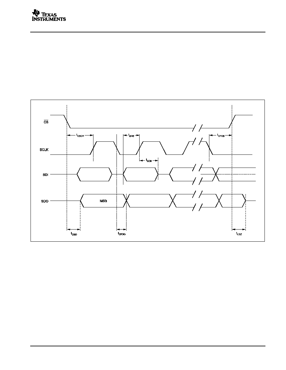
SERIAL CONTROL PORT
The serial control port is utilized to program the gain set-
tings for the PGA2311. The serial control port includes
three input pins and one output pin. The inputs include
CS (pin 2), SDI (pin 3), and SCLK (pin 6). The sole output
pin is SDO (pin 7).
The CS pin functions as the chip select input. Data may
be written to the PGA2311 only when CS is LOW. SDI
is the serial data input pin. Control data is provided as
a 16-bit word at the SDI pin, 8 bits each for the left and
right channel gain settings.
Data is formatted as MSB first, straight binary code.
SCLK is the serial clock input. Data is clocked into SDI
on the rising edge of SCLK.
SDO is the serial data output pin, and is used when
daisy-chaining multiple PGA2311 devices. Daisy-chain
operation is described in detail later in this section. SDO
is a tri-state output, and assumes a high impedance state
when CS is HIGH.
The protocol for the serial control port is shown in
Figure 2. See Figure 3 for detailed timing specifications
for the serial control port.
Gain Byte Format is MSB First, Straight Binary
R0 is the Least Significant Bit of the Right Channel Gain Byte
R7 is the Most Significant Bit of the Right Channel Gain Byte
L0 is the Least Significant Bit of the Left Channel Gain Byte
L7 is the Most Significant Bit of the Left Channel Gain Byte
SDI is latched on the rising edge of SCLK.
SDO transitions on the falling edge of SCLK.
Figure 2. Serial Interface Protocol.
PGA2311
SBOS218A DECEMBER 2001 REVISED JUNE 2002
www.ti.com
9
GAIN SETTINGS
The gain for each channel is set by its corresponding
8bit code, either R[7:0] or L[7:0] (see Figure 2). The
gain code data is straight binary format. If we let N
equal the decimal equivalent of R[7:0] or L[7:0], then
the following relationships exist for the gain settings:
For N = 0:
Mute Condition. The input multiplexer is connected to
analog ground (AGNDR or AGNDL).
For N = 1 to 255:
Gain (dB) = 31.5 [0.5 w (255 N)]
This results in a gain range of +31.5dB (with N = 255)
to 95.5dB (with N = 1).
Changes in gain setting may be made with or without
zero crossing detection. The operation of the zero
crossing detector and timeout circuitry is discussed lat-
er in this data sheet.
Figure 3. Serial Interface Timing Requirements.
PGA2311
SBOS218A DECEMBER 2001 REVISED JUNE 2002
www.ti.com
10
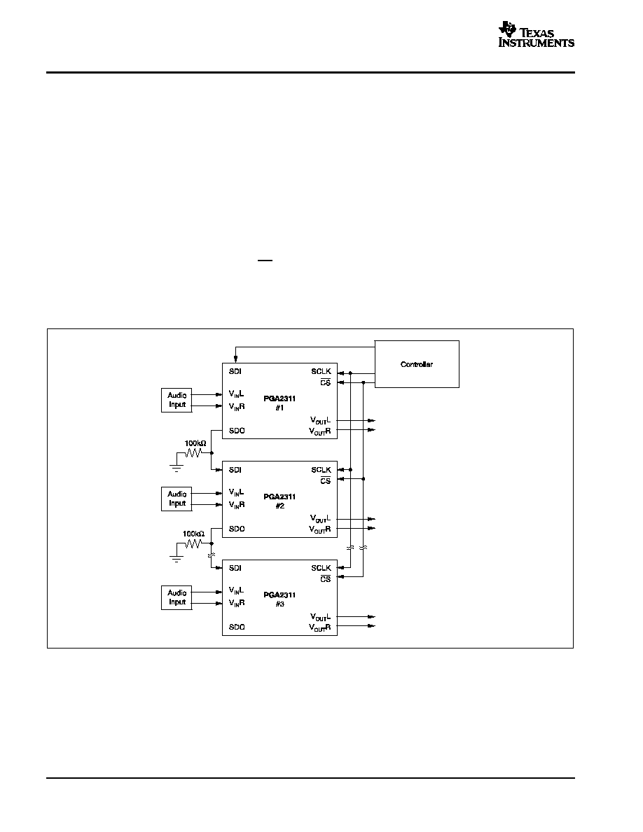
DAISY-CHAINING MULTIPLE PGA2311 DEVICES
In order to reduce the number of control signals re-
quired to support multiple PGA2311 devices on a
printed circuit board, the serial control port supports
daisy-chaining of multiple PGA2311 devices. Figure 4
shows the connection requirements for daisy-chain
operation. This arrangement allows a 3-wire serial in-
terface to control many PGA2311 devices.
As shown in Figure 4, the SDO pin from device #1 is con-
nected to the SDI input of device #2, and is repeated for
additional devices. This in turn forms a large shift regis-
ter, in which gain data may be written for all PGA2311s
connected to the serial bus. The length of the shift regis-
ter is 16
·
N bits, where N is equal to the number of
PGA2311 devices included in the chain. The CS input
must remain LOW for 16
·
N SCLK periods, where N is
the number of devices connected in the chain, in order
to allow enough SCLK cycles to load all devices.
ZERO CROSSING DETECTION
The PGA2311 includes a zero crossing detection func-
tion that can provide for noise-free level transitions.
The concept is to change gain settings on a zero cross-
ing of the input signal, thus minimizing audible glitches.
This function is enabled or disabled using the ZCEN in-
put (pin 1). When ZCEN is LOW, zero crossing detec-
tion is disabled. When ZCEN is HIGH, zero crossing
detection will be enabled.
The zero crossing detection takes effect with a change
in gain setting for a corresponding channel. The new
gain setting will not be implemented until either positive
slope zero crossing is detected or a time-out period of
16ms has elapsed. In the case of a time-out, the new
gain setting takes effect with no attempt to minimize
audible artifacts.
Figure 4. Daisy-Chaining Multiple PGA2311 Devices.
PGA2311
SBOS218A DECEMBER 2001 REVISED JUNE 2002
www.ti.com
11
MUTE FUNCTION
Muting can be achieved by either hardware or software
control. Hardware muting is accomplished via the
MUTE input, and software muting by loading all zeroes
into the volume control register.
MUTE disconnects the internal buffer amplifiers from
the output pins and terminates A
OUT
L and A
OUT
R with
10k
resistors to ground. The mute is activated with a
zero crossing detection (independent of the zero cross
enable status) or an 16ms time-out to eliminate any au-
dible "clicks" or "pops". MUTE also initiates an internal
offset calibration.
A software mute is implemented by loading all zeroes
into the volume control register. The internal amplifier
is set to unity gain with the amplifier input connected to
AGND.
APPLICATIONS INFORMATION
This section includes additional information that is per-
tinent to designing the PGA2311 into an end applica-
tion.
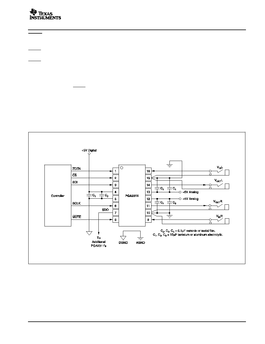
RECOMMENDED CONNECTION DIAGRAM
Figure 5 depicts the recommended connections for the
PGA2311. Power-supply bypass capacitors should be
placed as close to the PGA2311 package as physically
possible.
Figure 5. Recommended Connection Diagram.
PGA2311
SBOS218A DECEMBER 2001 REVISED JUNE 2002
www.ti.com
12
PRINTED CIRCUIT BOARD (PCB) LAYOUT
GUIDELINES
It is recommended that the ground planes for the digital
and analog sections of the PCB be separate from one
another. The planes should be connected at a single
point. Figure 6 shows the recommended PCB floor
plan for the PGA2311.
The PGA2311 is mounted so that it straddles the split
between the digital and analog ground planes. Pins 1
through 8 are oriented to the digital side of the board,
while pins 9 through 16 are on the analog side of the
board.
Figure 6. Typical PCB Layout Floor Plan.
PGA2311
SBOS218A DECEMBER 2001 REVISED JUNE 2002
www.ti.com
13
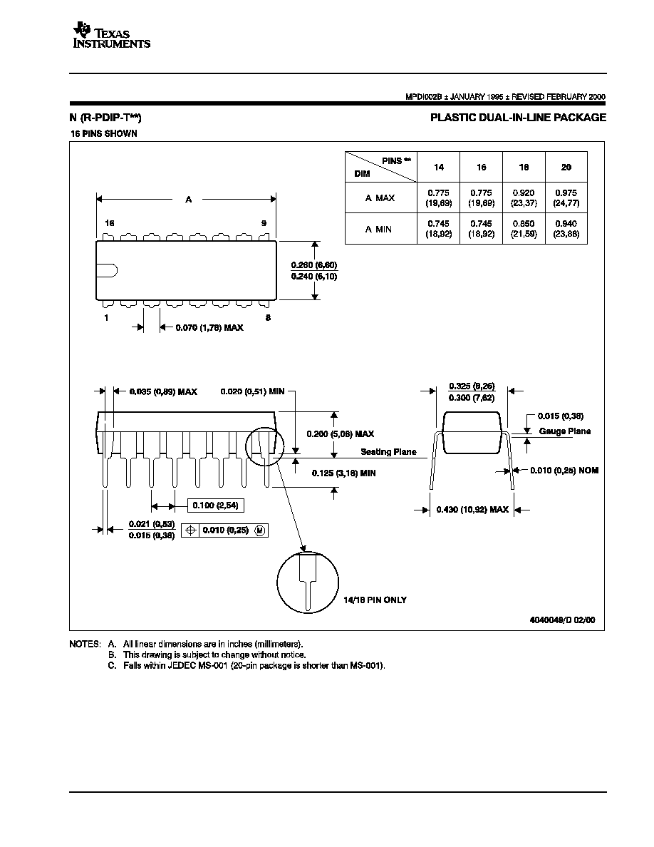
PACKAGE DRAWINGS
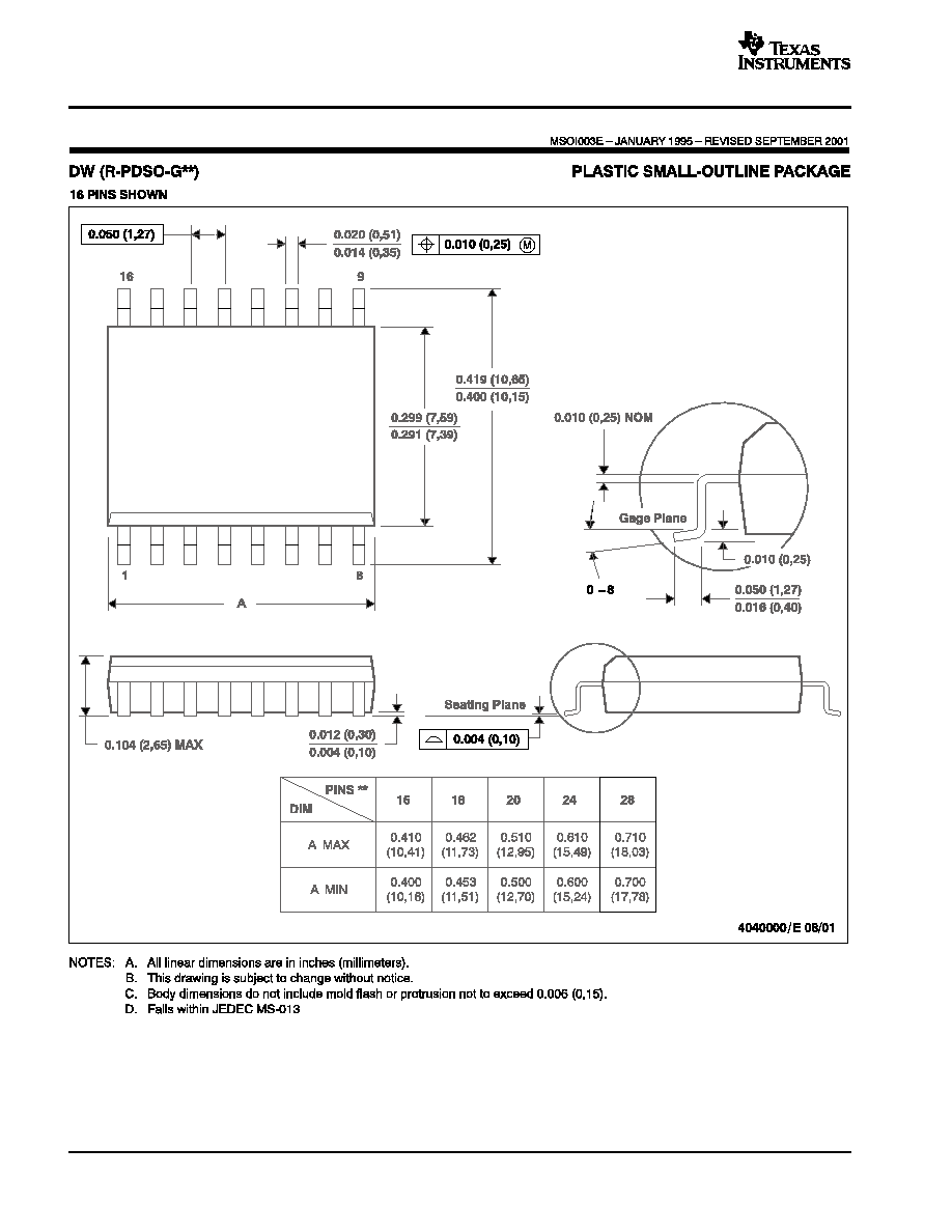
PGA2311
SBOS218A DECEMBER 2001 REVISED JUNE 2002
www.ti.com
14
PACKAGE DRAWINGS (Cont.)
PACKAGING INFORMATION
ORDERABLE DEVICE
STATUS(1)
PACKAGE TYPE
PACKAGE DRAWING
PINS
PACKAGE QTY
PGA2311P
ACTIVE
PDIP
N
16
25
PGA2311PA
ACTIVE
PDIP
N
16
25
PGA2311U
ACTIVE
SOIC
DW
16
48
PGA2311U/1K
ACTIVE
SOIC
DW
16
1000
PGA2311UA
ACTIVE
SOIC
DW
16
48
PGA2311UA/1K
ACTIVE
SOIC
DW
16
1000
(1) The marketing status values are defined as follows:
ACTIVE: Product device recommended for new designs.
LIFEBUY: TI has announced that the device will be discontinued, and a lifetime-buy period is in effect.
NRND: Not recommended for new designs. Device is in production to support existing customers, but TI does not recommend using this part in
a new design.
PREVIEW: Device has been announced but is not in production. Samples may or may not be available.
OBSOLETE: TI has discontinued the production of the device.
PACKAGE OPTION ADDENDUM
www.ti.com
3-Oct-2003

IMPORTANT NOTICE
Texas Instruments Incorporated and its subsidiaries (TI) reserve the right to make corrections, modifications,
enhancements, improvements, and other changes to its products and services at any time and to discontinue
any product or service without notice. Customers should obtain the latest relevant information before placing
orders and should verify that such information is current and complete. All products are sold subject to TI's terms
and conditions of sale supplied at the time of order acknowledgment.
TI warrants performance of its hardware products to the specifications applicable at the time of sale in
accordance with TI's standard warranty. Testing and other quality control techniques are used to the extent TI
deems necessary to support this warranty. Except where mandated by government requirements, testing of all
parameters of each product is not necessarily performed.
TI assumes no liability for applications assistance or customer product design. Customers are responsible for
their products and applications using TI components. To minimize the risks associated with customer products
and applications, customers should provide adequate design and operating safeguards.
TI does not warrant or represent that any license, either express or implied, is granted under any TI patent right,
copyright, mask work right, or other TI intellectual property right relating to any combination, machine, or process
in which TI products or services are used. Information published by TI regarding third-party products or services
does not constitute a license from TI to use such products or services or a warranty or endorsement thereof.
Use of such information may require a license from a third party under the patents or other intellectual property
of the third party, or a license from TI under the patents or other intellectual property of TI.
Reproduction of information in TI data books or data sheets is permissible only if reproduction is without
alteration and is accompanied by all associated warranties, conditions, limitations, and notices. Reproduction
of this information with alteration is an unfair and deceptive business practice. TI is not responsible or liable for
such altered documentation.
Resale of TI products or services with statements different from or beyond the parameters stated by TI for that
product or service voids all express and any implied warranties for the associated TI product or service and
is an unfair and deceptive business practice. TI is not responsible or liable for any such statements.
Following are URLs where you can obtain information on other Texas Instruments products and application
solutions:
Products
Applications
Amplifiers
amplifier.ti.com
Audio
www.ti.com/audio
Data Converters
dataconverter.ti.com
Automotive
www.ti.com/automotive
DSP
dsp.ti.com
Broadband
www.ti.com/broadband
Interface
interface.ti.com
Digital Control
www.ti.com/digitalcontrol
Logic
logic.ti.com
Military
www.ti.com/military
Power Mgmt
power.ti.com
Optical Networking
www.ti.com/opticalnetwork
Microcontrollers
microcontroller.ti.com
Security
www.ti.com/security
Telephony
www.ti.com/telephony
Video & Imaging
www.ti.com/video
Wireless
www.ti.com/wireless
Mailing Address:
Texas Instruments
Post Office Box 655303 Dallas, Texas 75265
Copyright
2003, Texas Instruments Incorporated
Document Outline
- FEATURES
- APPLICATIONS
- DESCRIPTION
- ABSOLUTE MAXIMUM RATINGS(1)
- PACKAGE/ORDERING INFORMATION
- ELECTRICAL CHARACTERISTICS
- DEVICE INFORMATION
- PIN CONFIGURATION
- PIN ASSIGNMENTS
- TYPICAL CHARACTERISTICS
- GENERAL DESCRIPTION
- POWER
UP STATE
- ANALOG INPUTS AND OUTPUTS
- SERIAL CONTROL PORT
- GAIN SETTINGS
- DAISY- CHAINING MULTIPLE PGA2311 DEVICES
- ZERO CROSSING DETECTION
- MUTE\ FUNCTION
- APPLICATIONS INFORMATION
- RECOMMENDED CONNECTION DIAGRAM
- PRINTED CIRCUIT BOARD (PCB) LAYOUT GUIDELINES
- PACKAGE DRAWINGS
- N(R-PDIP-T**) PLASTIC DUAL-IN-LINE PACKAGE
- DW (R-PDSO-G**) PLASTIC SMALL-OUTLINE PACKAGE