 | –≠–ª–µ–∫—Ç—Ä–æ–Ω–Ω—ã–π –∫–æ–º–ø–æ–Ω–µ–Ω—Ç: PGA4311U2 | –°–∫–∞—á–∞—Ç—å:  PDF PDF  ZIP ZIP |
Document Outline
- FEATURES
- APPLICATIONS
- DESCRIPTION
- ABSOLUTE MAXIMUM RATINGS(1)
- PACKAGE/ORDERING INFORMATION
- ELECTRICAL CHARACTERISTICS
- DEVICE INFORMATION
- PIN CONFIGURATION
- PIN ASSIGNMENTS
- TYPICAL CHARACTERISTICS
- GENERAL DESCRIPTION
- POWERÖUP STATE
- ANALOG INPUTS AND OUTPUTS
- SERIAL CONTROL PORT
- GAIN SETTINGS
- DAISY- CHAINING MULTIPLE PGA4311 DEVICES ZERO CROSSING DETECTION
- MUTE\ FUNCTION
- APPLICATIONS INFORMATION
- RECOMMENDED CONNECTION DIAGRAM
- PRINTED CIRCUIT BOARD (PCB) LAYOUT GUIDE-LINES
- PACKAGE DRAWING
- DW (R-PDSO-G**) PLASTIC SMALL-OUTLINE PACKAGE
SBOS230A ≠ MARCH 2002 ≠ REVISED JUNE 2002
4 Channel Audio Volume Control
PGA4311
1
FEATURES
D
DIGITALLY-CONTROLLED ANALOG VOLUME
CONTROL:
Four Independent Audio Channels
Serial Control Interface
Zero Crossing Detection
Mute Function
D
WIDE GAIN AND ATTENUATION RANGE:
+31.5dB to ≠95.5dB with 0.5dB Steps
D
LOW NOISE AND DISTORTION:
120dB Dynamic Range
0.0004% THD+N at 1kHz (U≠Grade)
0.0002% THD+N at 1kHz (A≠Grade)
D
NOISE-FREE LEVEL TRANSITIONS
D
LOW INTERCHANNEL CROSSTALK:
≠130dBFS
D
POWER SUPPLIES:
±
5V Analog, +5V Digital
D
AVAILABLE IN AN SOP-28 PACKAGE
APPLICATIONS
D
AUDIO AMPLIFIERS
D
MIXING CONSOLES
D
MULTI≠TRACK RECORDERS
D
BROADCAST STUDIO EQUIPMENT
D
MUSICAL INSTRUMENTS
D
EFFECTS PROCESSORS
D
A/V RECEIVERS
D
CAR AUDIO SYSTEMS
DESCRIPTION
The PGA4311 is a high≠performance, 4-channel audio
volume control designed for professional and high-end
consumer audio systems. Using high performance
operational amplifier stages internal to the PGA4311
yields low noise and distortion, while providing the
capability to drive 600
loads directly without buffering.
The 3-wire serial control interface allows for connection
to a wide variety of host controllers, in addition to
support for daisy-chaining of multiple PGA4311
devices.
www.ti.com
Please be aware that an important notice concerning availability, standard warranty, and use in critical applications of Texas Instruments
semiconductor products and disclaimers thereto appears at the end of this data sheet.
Copyright
2002, Texas Instruments Incorporated
PRODUCTION DATA information is current as of publication date. Products
conform to specifications per the terms of Texas Instruments standard warranty.
Production processing does not necessarily include testing of all parameters.
Please be aware that an important notice concerning availability, standard warranty, and use in critical applications of Texas Instruments
semiconductor products and disclaimers thereto appears at the end of this data sheet.
PGA4311
SBOS230A ≠ MARCH 2002 ≠ REVISED JUNE 2002
www.ti.com
2
ABSOLUTE MAXIMUM RATINGS
(1)
Supply Voltage, VA+
+5.5V
. . . . . . . . . . . . . . . . . . . . . . . . . . . .
VA≠
≠5.5V
. . . . . . . . . . . . . . . . . . . . . . . . . . . . . . . . . . . . . .
VD+
+5.5V
. . . . . . . . . . . . . . . . . . . . . . . . . . . . . . . . . . . . . .
VA+ to VD+
<
±
0.3V
. . . . . . . . . . . . . . . . . . . . . . . . . . . . . . . . .
Analog Input Voltage
0V to VA+, VA≠
. . . . . . . . . . . . . . . . . . . . . .
Digital Input Voltage
≠0.3V to VD+
. . . . . . . . . . . . . . . . . . . . . . . . .
Operating Temperature Range
≠40
∞
C to +85
∞
C
. . . . . . . . . . . . . . . .
Storage Temperature Range
≠65
∞
C to +150
∞
C
. . . . . . . . . . . . . . . .
Junction Temperature
+150
∞
C
. . . . . . . . . . . . . . . . . . . . . . . . . . .
Lead Temperature (soldering, 10s)
+300
∞
C
. . . . . . . . . . . . . . . . . . .
Package Temperature (IR reflow, 10s)
+235
∞
C
. . . . . . . . . . . . . . . . .
(1) Stresses above these ratings may cause permanent damage.
Exposure to absolute maximum conditions for extended periods
may degrade device reliability.
ELECTROSTATIC
DISCHARGE SENSITIVITY
This integrated circuit can be damaged by ESD. Texas
Instruments recommends that all integrated circuits be
handled with appropriate precautions. Failure to ob-
serve proper handling and installation procedures can
cause damage.
ESD damage can range from subtle performance
degradation to complete device failure. Precision
integrated circuits may be more susceptible to damage
because very small parametric changes could cause
the device not to meet its published specifications.
PACKAGE/ORDERING INFORMATION
PRODUCT
PACKAGE≠LEAD
PACKAGE
DESIGNATOR(1)
OPERATING
TEMPERATURE
RANGE
PACKAGE
MARKING
ORDERING
NUMBER
TRANSPORT
MEDIA, QUANTITY
PGA4311 (U Grade)
SOP 28
DW
40
∞
C to +85
∞
C
PGA4311U
PGA4311U
Rails
PGA4311 (U≠Grade)
SOP≠28
DW
≠40
∞
C to +85
∞
C
PGA4311U
PGA4311U/1K
Tape and Reel, 1000
PGA4311 (A Grade)
SOP 28
DW
40
∞
C to +85
∞
C
PGA4311UA
PGA4311UA
Rails
PGA4311 (A≠Grade)
SOP≠28
DW
≠40
∞
C to +85
∞
C
PGA4311UA
PGA4311UA/1K
Tape and Reel, 1000
(1) For the most current specifications and package information, refer to our web site at www. ti.com.
ELECTRICAL CHARACTERISTICS
At TA = +25
∞
C, VA+ = +5V, VA≠ = ≠5V, VD+ = +5V, RL = 100k
, CL = 20pF, BW measure = 10Hz to 20kHz, unless otherwise noted.
PARAMETER
CONDITIONS
PGA4311U (U≠Grade)
PGA4311UA (A≠Grade)
UNITS
PARAMETER
CONDITIONS
MIN
TYP
MAX
MIN
TYP
MAX
UNITS
DC CHARACTERISTICS
Step Size
0.5
0.5
dB
Gain Error
Gain Setting = 31.5dB
±
0.05
±
0.05
dB
Gain Matching
±
0.05
±
0.05
dB
Input Resistance
10
10
k
Input Capacitance
3
3
pF
AC CHARACTERISTICS
THD+N
VIN = 2Vrms, f = 1kHz
0.0004
0.001
0.0002
0.0004
%
Dynamic Range
VIN = AGND, Gain = 0dB
116
120
116
120
dB
Voltage Range, Output
(VA≠) +
1.25
(VA+) ≠
1.25
(VA≠) +
1.25
(VA+) ≠
1.25
V
Voltage Range, Input (without clipping)
2.5
2.5
Vrms
Output Noise
VIN = AGND, Gain = 0dB
2.5
4
2.5
4
µ
Vrms
Interchannel Crosstalk
f = 1kHz
≠130
≠130
dBFS
OUTPUT BUFFER
Offset Voltage
VIN = AGND, Gain = 0dB
0.25
0.5
0.25
0.5
mV
Load Capacitance Stability
100
100
pF
Short≠Circuit Current
50
50
mA
Unity≠Gain Bandwidth, Small Signal
10
10
MHz
PGA4311
SBOS230A ≠ MARCH 2002 ≠ REVISED JUNE 2002
www.ti.com
3
ELECTRICAL CHARACTERISTICS
(Cont.)
At TA = +25
∞
C, VA+ = +5V, VA≠ = ≠5V, VD+ = +5V, RL = 100k
, CL = 20pF, BW measure = 10Hz to 20kHz, unless otherwise noted.
PARAMETER
CONDITIONS
PGA4311U (U≠Grade)
PGA4311UA (A≠Grade)
UNITS
PARAMETER
CONDITIONS
MIN
TYP
MAX
MIN
TYP
MAX
UNITS
DIGITAL CHARACTERISTICS
High≠Level Input Voltage, VIH
+2.0
VD+
+2.0
VD+
V
Low≠Level Input Voltage, VIL
≠0.3
0.8
≠0.3
0.8
V
High≠Level Output Voltage, VOH
IO = 200
µ
A
(VA+) ≠
1.0
(VD+) ≠
1.0
V
Low≠Level Output Voltage, VOL
IO = ≠3.2mA
0.4
0.4
V
Input Leakage Current
1
10
1
10
µ
A
SWITCHING CHARACTERISTICS
Serial Clock (SCLK) Frequency
fSCLK
0
6.25
0
6.25
MHz
Serial Clock (SCLK) Pulse Width LOW
tPH
80
80
ns
Serial Clock (SCLK) Pulse Width HIGH
tPL
80
80
ns
MUTE Pulse Width LOW
tMI
2.0
2.0
ms
Input Timing
SDI Setup Time
tSDS
20
20
ns
SDI Hold Time
tSDH
20
20
ns
CS Falling to SCLK Rising
tCSCR
90
90
ns
SCLK Falling to CS Rising
tCFCS
35
35
ns
Output Timing
CS LOW to SDO Active
tCSO
35
35
ns
SCLK Falling to SDO Data Valid
tCFDO
60
60
ns
CS HIGH to SDO High Impedance
tCSZ
100
100
ns
POWER SUPPLY
Operating Voltage
VA+
+4.75
+5
+5.25
+4.75
+5
+5.25
V
VA≠
≠4.75
≠5
≠5.25
≠4.75
≠5
≠5.25
V
VD+
+4.75
+5
+5.25
+4.75
+5
+5.25
V
Quiescent Current
IA+
VA+ = +5V
17
22
17
22
mA
IA≠
VA≠ = ≠5V
19
24
19
24
mA
ID+
VD+ = +5V
0.5
1.0
0.5
1.0
mA
Power≠Supply Rejection Ratio PSRR (250Hz)
100
100
dB
TEMPERATURE RANGE
Operating Range
≠40
+85
≠40
+85
∞
C
Storage Range
≠65
+150
≠65
+150
∞
C

PGA4311
SBOS230A ≠ MARCH 2002 ≠ REVISED JUNE 2002
www.ti.com
4
PIN CONFIGURATION
Top View
SO
PIN ASSIGNMENTS
PIN
NAME
FUNCTION
1
MUTE
Mute Control Input (Active LOW)
2
AGND_1
Analog Ground, Channel 1
3
AIN_1
Analog Input, Channel 1
4
AGND_1
Analog Ground, Channel 1
5
AOUT_1
Analog Output, Channel 1
6
VA≠
Analog Power Supply, ≠5V
7
VA+
Analog Power Supply, +5V
8
AOUT_3
Analog Output, Channel 3
9
AGND_3
Analog Ground, Channel 3
10
AIN_3
Analog Input, Channel 3
11
AGND_3
Analog Ground, Channel 3
12
VD+
Digital Power Supply, +5V
13
SDI
Serial Data Input
14
CS
Chip Select Input
15
SCLK
Serial Clock Input
16
SDO
Serial Data Output
17
DGND
Digital Ground
18
AGND_4
Analog Ground, Channel 4
19
AIN_4
Analog Input, Channel 4
20
AGND_4
Analog Ground, Channel 4
21
AOUT_4
Analog Output, Channel 4
22
VA+
Analog Power Supply, +5V
23
VA≠
Analog Power Supply, ≠5V
24
AOUT_2
Analog Output, Channel 2
25
AGND_2
Analog Ground, Channel 2
26
AIN_2
Analog Input, Channel 2
27
AGND_2
Analog Ground, Channel 2
28
ZCEN
Zero Crossing Enable (Active HIGH)
PGA4311
SBOS230A ≠ MARCH 2002 ≠ REVISED JUNE 2002
www.ti.com
5
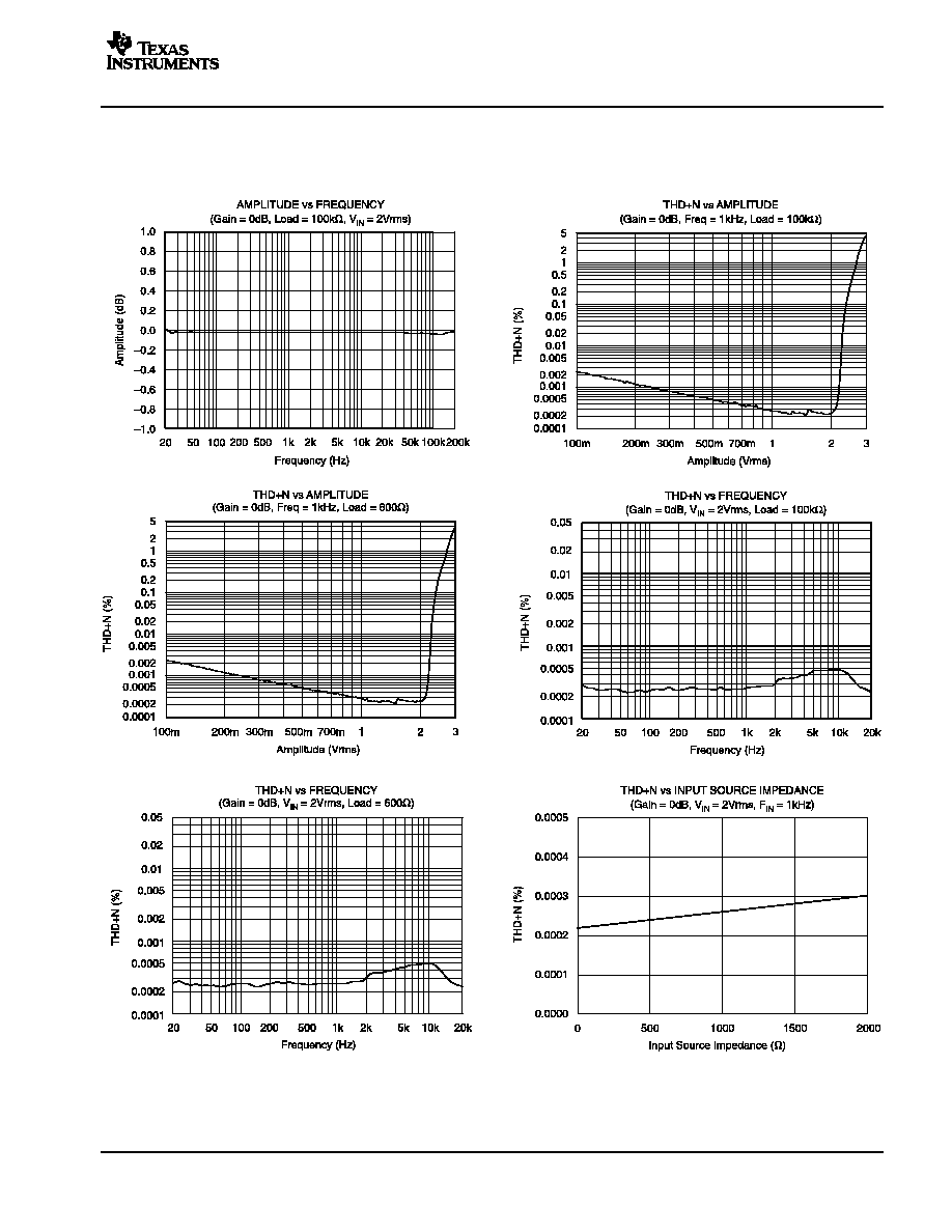
TYPICAL CHARACTERISTICS
At TA = +25
∞
C, VA+ = +5V, VA≠ = ≠5V, VD+ = +5V, RL = 100k
, CL = 20pF, BW measure = 10Hz to 20kHz, unless otherwise noted.
(NOTE: All plots taken with PGA4311 A≠Grade.)