Document Outline
- FEATURES
- APPLICATIONS
- DESCRIPTION
- FUNCTIONAL BLOCK DIAGRAM
- PACKAGE/ORDERING INFORMATION
- ABSOLUTE MAXIMUM RATINGS
- ELECTRICAL CHARACTERISTICS
- DEVICE INFORMATION
- PIN ASSIGNMENTS
- Terminal Functions
- TYPICAL PERFORMANCE CURVES
- THEORY OF OPERATION
- MASTER CLOCK AND SYSTEM CLOCK OUTPUT
- POWER-ON RESET
- FUNCTION CONTROL
- PLL1705 (Parallel Mode)
- Sampling Frequency Group Select
- Sampling Rate Select
- PLL1706 (Serial Mode)
- Program-Register Bit Mapping
- Mode Register
- CONNECTION DIAGRAM
- MPEG-2 APPLICATIONS
- BLOCK DIAGRAM OF MPEG-2 BASED SYSTEM APPLICATION
- MECHANICAL DATA
- DBQ (R-PDSO-G**) PLASTIC SMALL-OUTLINE PACKAGE
- IMPORTANT NOTICE
PLL1705
PLL1706
SLES046A ≠ AUGUST 2002 ≠ REVISED SEPTEMBER 2002
3.3-V DUAL PLL MULTICLOCK GENERATOR
FEATURES
D
27-MHz Master Clock Input
D
Generated Audio System Clock:
≠ SCKO0: 768 f
S
(f
S
= 44.1 kHz)
≠ SCKO1: 384 f
S
, 768 f
S
(f
S
= 44.1 kHz)
≠ SCKO2: 256 f
S
(f
S
= 32, 44.1, 48, 64, 88.2,
96 kHz)
≠ SCKO3: 384 f
S
(f
S
= 32, 44.1, 48, 64, 88.2,
96 kHz)
D
Zero PPM Error Output Clocks
D
Low Clock Jitter: 50 ps (Typical)
D
Multiple Sampling Frequencies:
≠ f
S
= 32, 44.1, 48, 64, 88.2, 96 kHz
D
3.3-V Single Power Supply
D
PLL1705: Parallel Control
PLL1706: Serial Control
D
Package: 20-Pin SSOP (150 mil), Lead-Free
Product
APPLICATIONS
D
DVD Players
D
DVD Add-On Cards for Multimedia PCs
D
Digital HDTV Systems
D
Set-Top Boxes
DESCRIPTION
The PLL1705
and PLL1706
are low cost, phase-locked
loop (PLL) multiclock generators. The PLL1705 and
PLL1706 can generate four system clocks from a 27-MHz
reference input frequency. The clock outputs of the
PLL1705 can be controlled by sampling frequency-control
pins and those of the PLL1706 can be controlled through
serial-mode control pins. The device gives customers both
cost and space savings by eliminating external
components and enables customers to achieve the very
low-jitter performance needed for high performance audio
DACs and/or ADCs. The PLL1705 and PLL1706 are ideal
for MPEG-2 applications which use a 27-MHz master
clock such as DVD players, DVD add-on cards for
multimedia PCs, digital HDTV systems, and set-top
boxes.
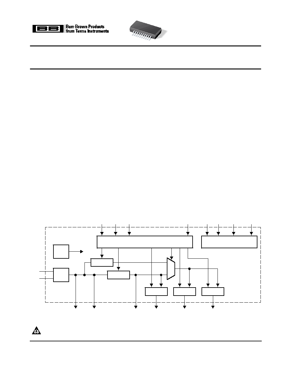
FUNCTIONAL BLOCK DIAGRAM
Mode Control Interface
( ): PLL1706
XT1
(ML)
SR
(MC)
FS2
(MD)
FS1
CSEL
PLL2
PLL1
OSC
XT2
MCKO1
MCKO2
SCKO0
Divider
Divider
Divider
SCKO1
SCKO2
SCKO3
Reset
Power Supply
VCC AGND VDD1≠3 DGND1≠3
Please be aware that an important notice concerning availability, standard warranty, and use in critical applications of Texas Instruments
semiconductor products and disclaimers thereto appears at the end of this data sheet.
Copyright
2002, Texas Instruments Incorporated
PRODUCTION DATA information is current as of publication date. Products
conform to specifications per the terms of Texas Instruments standard warranty.
Production processing does not necessarily include testing of all parameters.
The PLL1705 and PLL1706 use the same die and they are electrically identical except for mode control.
PLL1705
PLL1706
SLES046A ≠ AUGUST 2002 ≠ REVISED SEPTEMBER 2002
www.ti.com
2
This integrated circuit can be damaged by ESD. Texas Instruments recommends that all integrated circuits be handled with appropriate
precautions. Failure to observe proper handling and installation procedures can cause damage.
ESD damage can range from subtle performance degradation to complete device failure. Precision integrated circuits may be more susceptible to
damage because very small parametric changes could cause the device not to meet its published specifications.
PACKAGE/ORDERING INFORMATION
PRODUCT
PACKAGE
PACKAGE CODE
OPERATION
TEMPERATURE
RANGE
PACKAGE
MARKING
ORDERING
NUMBER
TRANSPORT
MEDIA
PLL1705DBQ
SSOP 20
20DBQ
25
∞
C to 85
∞
C
PLL1705
PLL1705DBQ
Tube
PLL1705DBQ
SSOP 20
20DBQ
≠25
∞
C to 85
∞
C
PLL1705
PLL1705DBQR
Tape and reel
PLL1706DBQ
SSOP 20
20DBQ
25
∞
C to 85
∞
C
PLL1706
PLL1706DBQ
Tube
PLL1706DBQ
SSOP 20
20DBQ
≠25
∞
C to 85
∞
C
PLL1706
PLL1706DBQR
Tape and reel
ABSOLUTE MAXIMUM RATINGS
over operating free-air temperature range unless otherwise noted(1)
PLL1705 AND PLL1706
Supply voltage: VCC, VDD1≠3
4 V
Supply voltage differences: VCC, VDD1≠3
±
0.1 V
Ground voltage differences: AGND, DGND1
≠
3
±
0.1 V
Digital input voltage: FS1 (MD), FS2 (MC), SR (ML), CSEL
≠
0.3 V to (VDD + 0.3) V
Analog input voltage, XT1, XT2
≠
0.3 V to (VCC + 0.3) V
Input current (any pins except supplies)
±
10 mA
Ambient temperature under bias
≠
40
∞
C to 125
∞
C
Storage temperature
≠55
∞
C to 150
∞
C
Junction temperature
150
∞
C
Lead temperature (soldering)
260
∞
C, 5 s
Package temperature (IR reflow, peak)
260
∞
C
(1) Stresses beyond those listed under "absolute maximum ratings" may cause permanent damage to the device. These are stress ratings only, and
functional operation of the device at these or any other conditions beyond those indicated under "recommended operating conditions" is not
implied. Exposure to absolute-maximum-rated conditions for extended periods may affect device reliability.
PLL1705
PLL1706
SLES046A ≠ AUGUST 2002 ≠ REVISED SEPTEMBER 2002
www.ti.com
3
ELECTRICAL CHARACTERISTICS
all specifications at TA = 25
∞
C, VDD1
≠
VDD3 (= VDD) = VCC = 3.3 V, fM = 27 MHz, crystal oscillation, fS = 48 kHz (unless otherwise noted)
PARAMETER
TEST CONDITIONS
MIN
TYP
MAX
UNIT
DIGITAL INPUT/OUTPUT
Logic input
CMOS compatible
VIH (1)
Input logic level
0.7VDD
3.6
Vdc
VIL (1)
Input logic level
0.3 VDD
Vdc
IIH (1)
Input logic current
VIN = VDD
65
100
µ
A
IIL (1)
Input logic current
VIN = 0 V
±
10
µ
A
Logic output
CMOS
VOH (2)
Output logic level
IOH = ≠4 mA
VDD ≠ 0.4 V
Vdc
VOL (2)
Output logic level
IOL = 4 mA
0.4
Vdc
Samplingfrequency
Standard fS
32
44.1
48
kHz
Sampling frequency
Double fS
64
88.2
96
kHz
MASTER CLOCK (MCKO1, 2) CHARACTERISTICS (fM = 27 MHz, C1 = C2 = 15 pF, CL = 20 pF on measurement pin)
Master clock frequency
26.73
27
27.27
MHz
VIH
Input level(3)
0.7 VCC
V
VIL
Input level(3)
0.3 VCC
V
IIH
Input current(3)
VIN = VCC
±
10
µ
A
IIL
Input current(3)
VIN = 0 V
±
10
µ
A
Output voltage (4)
3.5
Vp-p
Output rise time
20% to 80% of VDD
2.0
ns
Output fall time
80% to 20% of VDD
2.0
ns
Duty cycle
For crystal oscillation
45%
48%
55%
Duty cycle
For external clock
50%
Clock jitter (5)
50
ps
Power-up time (6)
0.5
1.5
ms
PLL AC CHARACTERISTICS (SCKO0
≠
3) (fM = 27 MHz, CL = 20 pF on measurement pin)
SCKO0
Fixed
33.8688
SCKO1
Output system clock frequency
Selectable for 44.1 kHz
16.9344
33.8688
MHz
SCKO2
Output system clock frequency
256 fS
8.192
12.288
24.576
MHz
SCKO3
384 fS
12.288
18.432
36.864
Output rise time
20% to 80% of VDD
2.0
ns
Output fall time
80% to 20% of VDD
2.0
ns
Output duty cycle
45
50
55
%
Output clock jitter (5)
50
100
ps
Frequency Settling Time(7)
PLL1705, to stated output frequency
50
150
ns
Frequency Settling Time(7)
PLL1706, to stated output frequency
80
200
ns
Power-up time (8)
To stated output frequency
3
6
ms
(1) Pins 5, 6, 7, 12: FS1/MD, FS2/MC, SR/ML, CSEL (Schmitt-trigger input with internal pulldown, 3.3-V tolerant)
(2) Pins 2, 3, 14, 15, 18, 19: SCKO2, SCKO3, MCKO1, MCKO2, SCKO1, SCKO0
(3) Pin 10: XT1
(4) Pin 11: XT2
(5) Jitter performance is specified as standard deviation of jitter for 27-MHz crystal oscillation and default SCKO frequency setting. Jitter
performance varies with master clock mode, SCKO frequency setting and load capacitance on each clock output.
(6) The delay time from power on to oscillation
(7) The settling time when the sampling frequency is changed
(8) The delay time from power on to lockup
(9) fM = 27-MHz crystal oscillation, no load on MCKO1, MCKO2, SCKO0, SCKO1, SCKO2, SCKO3. Power supply current varies with sampling
frequency selection and load condition.
(10) While all bits of CE[6:1] are 0, the PLL1706 goes into power-down mode.

PLL1705
PLL1706
SLES046A ≠ AUGUST 2002 ≠ REVISED SEPTEMBER 2002
www.ti.com
4
ELECTRICAL CHARACTERISTICS(continued)
all specifications at TA = 25
∞
C, VDD1
≠
VDD3 (= VDD) = VCC = 3.3 V, fM = 27 MHz, crystal oscillation, fS = 48 kHz (unless otherwise noted)
PARAMETER
UNIT
MAX
TYP
MIN
TEST CONDITIONS
POWER SUPPLY REQUIREMENTS
VCC, VDD
Supply voltage range
2.7
3.3
3.6
Vdc
IDD + ICC
Supply current (9)
VDD = VCC = 3.3 V, fS = 48 kHz
19
25
mA
IDD + ICC
Supply current (9)
Power down(10)
320
500
µ
A
Power dissipation
VDD = VCC = 3.3 V, fS = 48 kHz
63
90
mW
TEMPERATURE RANGE
Operating temperature
≠25
85
∞
C
JA
Thermal resistance
PLL1705/6DBQ: 20-pin SSOP (150 mil)
150
∞
C/W
(1) Pins 5, 6, 7, 12: FS1/MD, FS2/MC, SR/ML, CSEL (Schmitt-trigger input with internal pulldown, 3.3-V tolerant)
(2) Pins 2, 3, 14, 15, 18, 19: SCKO2, SCKO3, MCKO1, MCKO2, SCKO1, SCKO0
(3) Pin 10: XT1
(4) Pin 11: XT2
(5) Jitter performance is specified as standard deviation of jitter for 27-MHz crystal oscillation and default SCKO frequency setting. Jitter
performance varies with master clock mode, SCKO frequency setting and load capacitance on each clock output.
(6) The delay time from power on to oscillation
(7) The settling time when the sampling frequency is changed
(8) The delay time from power on to lockup
(9) fM = 27-MHz crystal oscillation, no load on MCKO1, MCKO2, SCKO0, SCKO1, SCKO2, SCKO3. Power supply current varies with sampling
frequency selection and load condition.
(10) While all bits of CE[6:1] are 0, the PLL1706 goes into power-down mode.
PIN ASSIGNMENTS
1
2
3
4
5
6
7
8
9
10
20
19
18
17
16
15
14
13
12
11
V
DD
1
SCKO2
SCKO3
DGND1
FS1
FS2
SR
V
CC
AGND
XT1
V
DD
3
SCKO0
SCKO1
DGND3
DGND2
MCKO2
MCKO1
V
DD
2
CSEL
XT2
PLL1705
(TOP VIEW)
1
2
3
4
5
6
7
8
9
10
20
19
18
17
16
15
14
13
12
11
V
DD
1
SCKO2
SCKO3
DGND1
MD
MC
ML
V
CC
AGND
XT1
V
DD
3
SCKO0
SCKO1
DGND3
DGND2
MCKO2
MCKO1
V
DD
2
CSEL
XT2
PLL1706
(TOP VIEW)

PLL1705
PLL1706
SLES046A ≠ AUGUST 2002 ≠ REVISED SEPTEMBER 2002
www.ti.com
5
Terminal Functions
TERMINAL
I/O
DESCRIPTION
NAME
NO.
I/O
DESCRIPTION
AGND
9
≠
Analog ground
CSEL
12
IN
SCKO1 frequency selection control(1)
DGND1
4
≠
Digital ground 1
DGND2
16
≠
Digital ground 2
DGND3
17
≠
Digital ground 3
FS1(MD)
5
IN
Sampling frequency group control in PLL1705, data input for serial control in PLL1706(1)
FS2(MC)
6
IN
Sampling frequency group control in PLL1705, bit clock input for serial control in PLL1706(1)
MCKO1
14
OUT
27-MHz master clock output 1
MCKO2
15
OUT
27-MHz master clock output 2
SCKO0
19
OUT
System clock output 0 (33.8688 MHz fixed)
SCKO1
18
OUT
System clock output 1 (selectable for 44.1 kHz)
SCKO2
2
OUT
System clock output 2 (256 fS)
SCKO3
3
OUT
System clock output 3 (384 fS)
SR(ML)
7
IN
Sampling rate control in PLL1705, load strobe input for serial control in PLL1706(1)
VCC
8
≠
Analog power supply, 3.3 V
VDD1
1
≠
Digital power supply 1, 3.3 V
VDD2
13
≠
Digital power supply 2, 3.3 V
VDD3
20
≠
Digital power supply 3, 3.3 V
XT1
10
IN
27-MHz crystal oscillator, or external clock input
XT2
11
OUT
27-MHz crystal oscillator, must be OPEN for external clock input mode
(1) Schmitt-trigger input with internal pulldown.