Standard Application
Ordering Information
Through-Hole
PT3101A = 5 Volts
PT3102A = 12 Volts
PT3103A = 15 Volts
Surface Mount
PT3101C = 5 Volts
PT3102C = 12 Volts
PT3103C = 15 Volts
(For dimensions and PC
board layout, see Package
Style 700.)
Pin-Out Information
Pin Function
1
Remote
ON/OFF
2
-V
in
3
+V
in
4
-V
out
5
+V
out
6
Do not connect
∑
Power Density 15 Watts/in
3
∑
Wide Input Voltage Range
36V to 75V
∑
80% Efficiency
∑
500 VDC Isolation
∑
Industry's Smallest Footprint
∑
Fast Transient Response
∑
No External Components Required
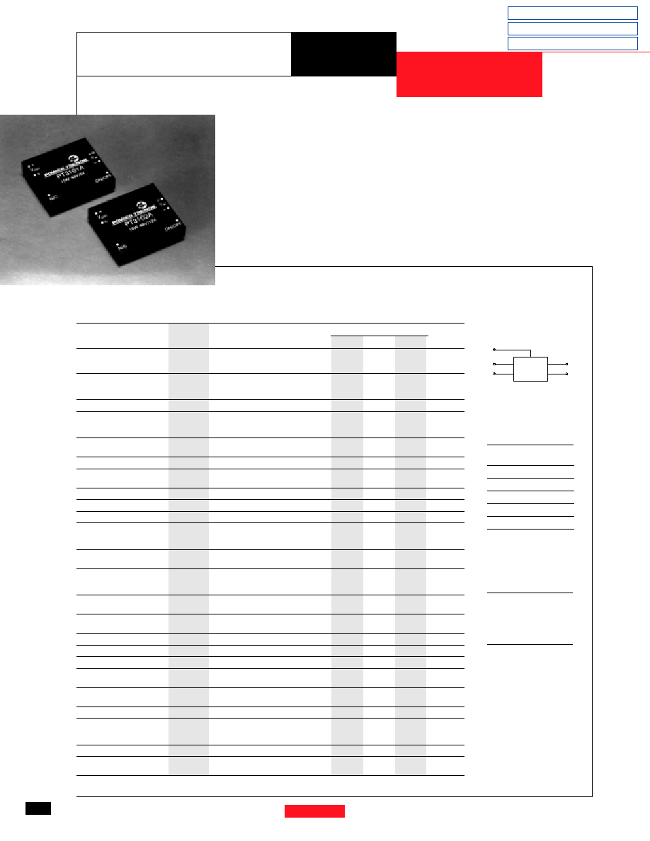
Power Trends' PT3101A (5V),
PT3102A (12V) and PT3103A (15V)
Isolated DC-DC Converters advance the
state-of-the-art for board-mounted con-
verters by employing high switching
frequencies greater than 650 KHz and
planar magnetics and surface-mount
construction. They feature the industry's
smallest footprint, a power density of
15 Watts/in
3
, and operate at 80% effi-
ciency. They are designed for Telecom,
Industrial, Computer, Medical, and other
distributed power applications requiring
input-to-output isolation.
P T 3 1 0 0 S e r i e s
For assistance or to order, call
(800) 531-5782
4 8 V
15 WATT 48V TO 5V/12V/15V
ISOLATED DC-DC CONVERTER
68
Power Trends, Inc.
27715 Diehl Road, Warrenville, IL 60555
(800) 531-5782
Fax: (630) 393-6902 http://www.powertrends.com
*
See Thermal Derating Curves
Specifications
Characteristics
PT3100 SERIES
(T
a
=25
∞C unless noted)
Symbols
Conditions
Min
Typ
Max
Units
Output Current
I
o
Over V
in
range
V
o
= 5V
0
--
3.0
A
V
o
= 12V
0
--
1.25
A
V
o
= 15V
0
--
1.0
A
Current Limit
I
cl
V
in
= 36V
V
o
= 5V
--
4.00
--
A
V
o
= 12V
--
1.75
--
A
V
o
= 15V
--
1.4
--
A
On/Off Standby Current
I
in standby
V
in
= 48V, Pin 1 = -V
in
--
7
10
mA
Short Circuit Current
I
sc
V
in
= 48V
V
o
= 5V
--
5.5
--
A
V
o
= 12V
--
3.5
--
A
V
o
= 15V
--
2.0
--
A
Inrush Current
I
ir
V
in
= 48V @ max I
o
--
0.6
1.0
A
t
ir
On start-up
--
1.0
5.0
mSec
Input Voltage Range
V
in
I
o
= 0.1 to max I
o
36.0
48.0
75.0
V
Output Voltage Tolerance
V
o
Over V
in
Range
T
A
= -20∞C to 70∞C
--
±1.0
±2.0
%V
o
Ripple Rejection
RR
Over V
in
range @ 120 Hz
--
60
--
dB
Line Regulation
Reg
line
Over V
in
range @ max I
o
--
±0.2
±1.0
%V
o
Load Regulation
Reg
load
10% to 100% of I
o
max
--
±0.4
±1.0
%V
o
V
o
Ripple/Noise
V
n
V
in
=48V, I
o
=3.0A,
V
o
=5V
--
75
100
mV
pp
V
in
=48V, I
o
=1.25A, V
o
=12V
--
120
150
mV
pp
V
in
=48V, I
o
=1.0A,
V
o
=15V
--
100
200
mV
pp
Transient Response
t
tr
50% load change
--
100
200
µSec
V
o
over/undershoot
--
3.0
5.0
%V
o
Efficiency
V
in
=48V, I
o
=3.0A, V
o
=5V
--
79
--
%
V
in
=48V, I
o
=1.25A, V
o
=12V
--
80
--
%
V
in
=48V, I
o
=1A, V
o
=15V
--
80
--
%
Switching Frequency
o
Over V
in
and I
o
,
V
o
=5V
800
850
900
kHz
V
o
=12V/15V
600
650
700
kHz
Recommended Operating
T
a
V
in
= 48V @ max I
o
-20
--
+70*
∞C
Temperature Range
Free air convection, (40-60LFM)
Thermal Resistance
ja
Free Air Convection, (40-60LFM)
--
16
--
∞C/W
Case Temperature
T
c
@ Thermal shutdown
--
--
100
∞C
Storage Temperature
T
s
--
-40
--
110
∞C
Mechanical Shock
--
Per Mil-STD-202F, Method 213B,
--
50
--
G's
6mS, Half-sine, mounted to a PCB
Mechanical Vibration
--
Per Mil-STD-202F, Method 204D,
--
10
--
G's
10-500Hz, Soldered in a PCB
Weight
--
--
--
28
--
grams
Isolation
--
--
500
--
--
V
Capacitance
--
--
--
1100
--
pF
Resistance
--
--
10
--
--
M
Flammability
--
Materials meet UL 94V-0
Remote On/Off
On
Open or 2.5 to 7.0 VDC above -V
in
Off
Short or 0 to 0.8 VDC above -V
in
+Vout
-Vout
-Vin
+Vin
3
2
4
5
On/Off
1
PT3100
Application Notes
Mechanical Outline
Product Selector Guide
Revised 8/13/98
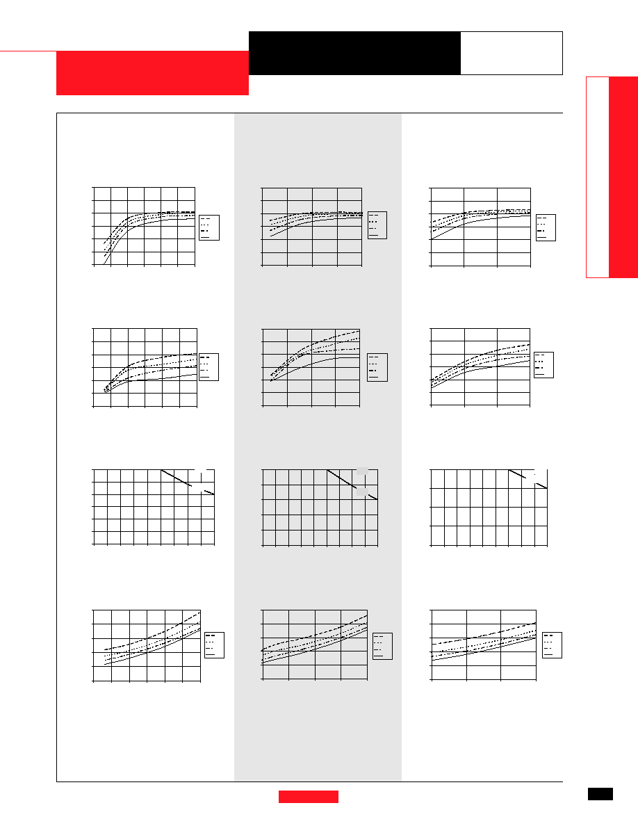
PT3102, 12.0 VDC
(See Note 1)
PT3103, 15.0 VDC
(See Note 1)
Efficiency vs Output Current
Efficiency vs Output Current
Efficiency vs Output Current
Ripple vs Output Current
Ripple vs Output Current
Ripple vs Output Current
Thermal Derating (T
a
)
(See Note 2)
Thermal Derating (T
a
)
(See Note 2)
Thermal Derating (T
a
)
(See Note 2)
Power Dissipation vs Output Current
Power Dissipation vs Output Current
Power Dissipation vs Output Current
Note 1:
All data listed in the above graphs, except for derating data, has been developed from actual products tested at 25∞C. This data is considered typical data for the DC-DC Converter.
Note 2:
Thermal derating graphs are developed in free air convection cooling of 40-60 LFM.
PT3101, 5.0 VDC
(See Note 1)
Efficiency - %
Ripple-(mV)
Iout-(Amps)
PD-(W
atts)
Efficiency - %
Efficiency - %
Ripple-(mV)
Ripple-(mV)
Iout-(Amps)
Iout-(Amps)
PD-(W
atts)
PD-(W
atts)
Iout-(Amps)
Iout-(Amps)
Iout-(Amps)
Iout-(Amps)
Iout-(Amps)
Vin-(Volts)
Vin-(Volts)
Vin-(Volts)
Iout-(Amps)
Iout-(Amps)
For assistance or to order, call
(800) 531-5782
C H A R A C T E R I S T I C D A T A
P T 3 1 0 0 S e r i e s
4 8 V
69
48V Bus Products
DA
T
A
SHEETS
Power Trends, Inc.
27715 Diehl Road, Warrenville, IL 60555
(800) 531-5782
Fax: (630) 393-6902 http://
www.powertrends.com
40
50
60
70
80
90
100
0
0.5
1
1.5
2
2.5
3
36V
48V
60V
72V
Vin
Iout-(Amps)
40
50
60
70
80
90
100
0.25
0.5
0.75
1
1.25
36V
48V
60V
72V
Vin
40
50
60
70
80
90
100
0.25
0.5
0.75
1
36V
48V
60V
72V
Vin
0
20
40
60
80
100
120
0.25
0.5
0.75
1
72V
60V
48V
36V
Vin
0
20
40
60
80
100
120
0.25
0.5
0.75
1
1.25
72V
60V
48V
36V
Vin
0
20
40
60
80
100
120
0
0.5
1
1.5
2
2.5
3
72V
60V
48V
36V
Vin
0
0.5
1
1.5
2
2.5
3
36
40
44
48
52
56
60
64
68
72
60∞
70∞
0
0.25
0.5
0.75
1
1.25
36
40
44
48
52
56
60
64
68
72
60∞
70∞
0
0.25
0.5
0.75
1
36
40
44
48
52
56
60
64
68
72
60∞
70∞
0
1
2
3
4
5
0.25
0.5
0.75
1
72V
60V
48V
36V
Vin
0
1
2
3
4
5
0.25
0.5
0.75
1
1.25
72V
60V
48V
36V
Vin
0
1
2
3
4
5
0
0.5
1
1.5
2
2.5
3
72V
60V
48V
36V
Vin
Iout-(Amps)

IMPORTANT NOTICE
Texas Instruments and its subsidiaries (TI) reserve the right to make changes to their products or to discontinue
any product or service without notice, and advise customers to obtain the latest version of relevant information
to verify, before placing orders, that information being relied on is current and complete. All products are sold
subject to the terms and conditions of sale supplied at the time of order acknowledgement, including those
pertaining to warranty, patent infringement, and limitation of liability.
TI warrants performance of its semiconductor products to the specifications applicable at the time of sale in
accordance with TI's standard warranty. Testing and other quality control techniques are utilized to the extent
TI deems necessary to support this warranty. Specific testing of all parameters of each device is not necessarily
performed, except those mandated by government requirements.
CERTAIN APPLICATIONS USING SEMICONDUCTOR PRODUCTS MAY INVOLVE POTENTIAL RISKS OF
DEATH, PERSONAL INJURY, OR SEVERE PROPERTY OR ENVIRONMENTAL DAMAGE ("CRITICAL
APPLICATIONS"). TI SEMICONDUCTOR PRODUCTS ARE NOT DESIGNED, AUTHORIZED, OR
WARRANTED TO BE SUITABLE FOR USE IN LIFE-SUPPORT DEVICES OR SYSTEMS OR OTHER
CRITICAL APPLICATIONS. INCLUSION OF TI PRODUCTS IN SUCH APPLICATIONS IS UNDERSTOOD TO
BE FULLY AT THE CUSTOMER'S RISK.
In order to minimize risks associated with the customer's applications, adequate design and operating
safeguards must be provided by the customer to minimize inherent or procedural hazards.
TI assumes no liability for applications assistance or customer product design. TI does not warrant or represent
that any license, either express or implied, is granted under any patent right, copyright, mask work right, or other
intellectual property right of TI covering or relating to any combination, machine, or process in which such
semiconductor products or services might be or are used. TI's publication of information regarding any third
party's products or services does not constitute TI's approval, warranty or endorsement thereof.
Copyright
©
1999, Texas Instruments Incorporated