 | –≠–ª–µ–∫—Ç—Ä–æ–Ω–Ω—ã–π –∫–æ–º–ø–æ–Ω–µ–Ω—Ç: PT4567N | –°–∫–∞—á–∞—Ç—å:  PDF PDF  ZIP ZIP |
For technical support and more information, see inside back cover or visit www.ti.com
PT4560 Series
30-W 48-V Input
Isolated DC/DC Converter
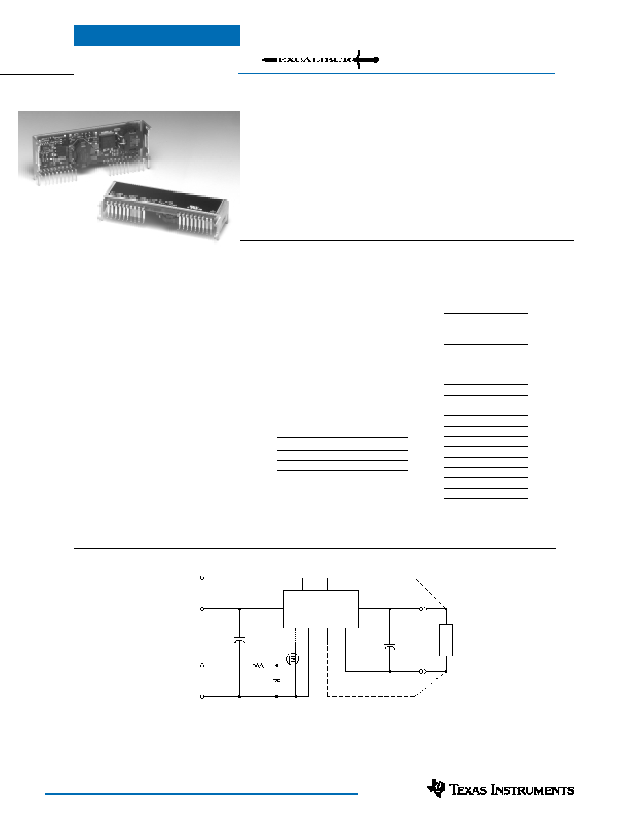
Standard Application
Cin
= Optional 100µF/100V electrolytic
Cout = Required 330µF electrolytic (See Notes)
Q
1
= N-Channel MOSFET
R
1
/C
1
= Optional (see application notes)
P T 4 5 6 0
2
1 9
7, 8, 9
1 4 - 1 7
4 - 6
1 0 - 1 2
1 3
L
O
A
D
C
I N
+
V
O
Adjust
+ V
I N
Inhibit
+ R E M O T E S E N S E
≠ R E M O T E S E N S E
+ V
O
≠ V
O
≠ V
I N
Q
1
C
O U T
+
1 8
R
1
C
1
Features
∑
Input Voltage Range:
36V to 75V
∑
1500 VDC Isolation
∑
On/Off Control
∑
V
o
Adjust
∑
Differential Remote Sense
∑
Current Limit
∑
Short-Circuit Protection
∑
Over-Temperature Shutdown
Description
The PT4560 series is a single-output
isolated DC/DC converter, housed in a
19-pin space-saving package. These mod-
ules are UL, CSA, and VDE approved
for telecom applications, and rated at
30 watts or 8 A. Standard output voltages
range from 1.8 V to 15 V, each adjustable
by up to ±10% of nominal.
Operating features include a remote
on/off control, an under-voltage-lockout
(UVLO), and a differential remote sense.
The PT4560 series also incorporates
many protection features. These include
output current limit, short-circuit pro-
tection, and over-temperature shutdown.
PT4560 requires a 330µF of output
capacitance for proper operation.
Ordering Information
PT4561
H = 3.3V/8A (26.4W)
PT4562
H = 5.0V/6A
PT4563
H = 12.0V/2.5A
PT4564
H = 15.0V/2A
PT4565
H = 2.0V/8A (16W)
PT4566
H = 2.5V/8A (20W)
PT4567
H = 1.8V/8A (14.4W)
PT4568
H = 5.2V/6A
PT4571
H = 9.0V/3.3A
Pin-Out Information
Pin Function
1
Do Not Use
2
Remote On/Off
3
Do Not Use
4
-Vin
5
-Vin
6
-Vin
7
+Vin
8
+Vin
9
+Vin
10
-Vo
11
-Vo
12
-Vo
13
-Remote Sense
14
+Vo
15
+Vo
16
+Vo
17
+Vo
18
Vo Adjust
19
+Remote Sense
For more information,
see application notes.
SLTS097C
(Revised 3/14/2002)
∑
Undervoltage Lockout
∑
Space-Saving Package
∑
Solderable Copper Case
∑
UL1950 Recognized
∑
CSA 22.2 950 Certified
∑
EN60950 Approved
∑
VDE Licensed
∑
4.9 x10
6
Hrs MTBF
∑
Meets FCC Class A
Radiated Limits
PT Series Suffix
(PT1234
x
)
Case/Pin
Order
Package
Configuration
Suffix
Code *
Vertical
N
(END)
Horizontal
A
(ENA)
SMD
C
(ENC)
* Previously known as package styles 1400 &
1410.
(Reference the applicable package code draw-
ing for the dimensions and PC board layout)

For technical support and more information, see inside back cover or visit www.ti.com
PT4560 Series
30-W 48-V Input
Isolated DC/DC Converter
Specifications
(Unless otherwise stated, T
a
=25∞C, V
in
=48V, C
out
=330µF, and I
o
=I
o
max)
PT4560 SERIES
Characteristic
Symbol
Conditions
Min
Typ
Max
Units
Output Current
I
o
Over V
in
range
V
o
= 15V
0.1
(1)
--
2.0
V
o
= 12V
0.1
(1)
--
2.5
A
V
o
= 9.0V
0.1
(1)
--
3.3
V
o
=5.0V
0.25
(1)
--
6.0
V
o
3.3V
0.25
(1)
--
8.0
Input Voltage Range
V
in
Over I
o
Range
36.0
48.0
75.0
V
Set Point Voltage Tolerance
V
o
tol
V
o
5.0V
--
±1
±1.5
%V
o
V
o
3.3V
--
±33
±50
mV
Temperature Variation
Reg
temp
≠40∞
T
a
+85∞C
--
±0.5
--
%V
o
Line Regulation
Reg
line
Over V
in
range
V
o
5.0V
--
±0.2
±1.0
%V
o
V
o
3.3V
--
±7
±33
mV
Load Regulation
Reg
load
Over I
o
range
Vo
5.0V
--
±0.4
±1.0
%V
o
V
o
3.3V
--
±13
±33
mV
Total Output Voltage Variation
V
o
tot
Includes set-point, line, load,
V
o
5.0V
--
±2
--
%V
o
≠40∞
T
a
+85∞C
V
o
3.3V
--
±67
--
mV
Efficiency
V
o
= 15V
--
85
--
V
o
= 12V
--
87
--
V
o
=9.0V
--
84
--
%
V
o
=5.0V
--
84
--
V
o
=3.3V
--
80
--
V
o
=1.8V
--
69
--
V
o
Ripple (pk-pk)
V
r
20MHz bandwidth
V
o
5.0V
--
1.0
2.0
%V
o
V
o
3.3V
--
50
75
mV
pp
Transient Response
t
tr
0.1A/µs load step, 50% to 100% I
o
max
--
100
200
µs
V
tr
V
o
over/undershoot
V
o
5.0V
--
±3.0
±5.0
%V
o
V
o
3.3V
--
±100
±150
mV
Short Circuit Current
I
sc
--
2xI
o
max
--
A
Switching Frequency
s
Over V
in
range
V
o
10V
400
500
600
kHz
V
o
<
10V
600
750
900
Under-Voltage Lockout
UVLO
V
in
increasing
--
34
--
V
V
in
decreasing
--
33
--
Remote On/Off Input (pin 2)
Referenced to ≠V
in
(pins 4≠6)
Input High Voltage
V
IH
2.5
--
15
(2)
V
Input Low Voltage
V
IL
≠0.2
--
+0.8
Input Low Current
I
IL
≠3
≠6
≠10
µA
Standby Input Current
I
in
standby
pins 2 & 4 connected
--
8
16
mA
Internal Input Capacitance
C
in
--
0.66
--
µF
External Output Capacitance
C
out
Between +V
o
and ≠V
o
V
o
9.0V
260
330
600
(3)
µF
V
o
5.0V
260
330
1,000
(3)
Isolation Voltage
Input-output/input-case
1500
--
--
Vdc
Capacitance
Input-output
--
1200
--
pF
Resistance
Input-output
10
--
--
M
Operating Temperature Range
T
a
Over V
in
range
-40
(4)
--
+85
(5)
∞C
Maximum Case Temperature
T
c
--
--
100
∞C
Storage Temperature Range
T
s
-40
--
+125
∞C
Reliability
MTBF
Per Bellcore TR-332
4.9
--
--
10
6
Hrs
50% stress, T
a
=40∞C, ground benign
Mechanical Shock
--
Per Mil-Std-883D, method 2002.3,
--
500
--
G's
1mS, half-sine, mounted to a fixture
Mechanical Vibration
--
Per Mil-Std-883D, method 2007.2,
--
20
--
G's
20-2000Hz, soldered in board
Weight
--
--
--
40
--
grams
Flammability
--
Materials meet UL 94V-0
Notes:
(1) The DC/DC converter will operate at no load with reduced specifications.
(2) The Remote On/Off input has an internal pull-up. If it is left open circuit the PT4560 will operate when input power is applied. A low-leakage
(<100nA) MOSFET is recommended to control this input. The open-circuit voltage is less than 10V. See application notes for interface considerations.
(3) Output capacitor values are absolute. Allowances must be made for any additional de-coupling capacitors and the total external capacitor tolerance.
The value of external capacitance is limited due to regulator startup current requirements. Consult the factory for further details.
(4) For operation below 0∞C, the required external output capacitor must have temperature stable characteristics. E.g. Tantalum or OsconÆ types.
(5) See Safe Operating Area curves or contact the factory for the appropriate thermal derating.

For technical support and more information, see inside back cover or visit www.ti.com
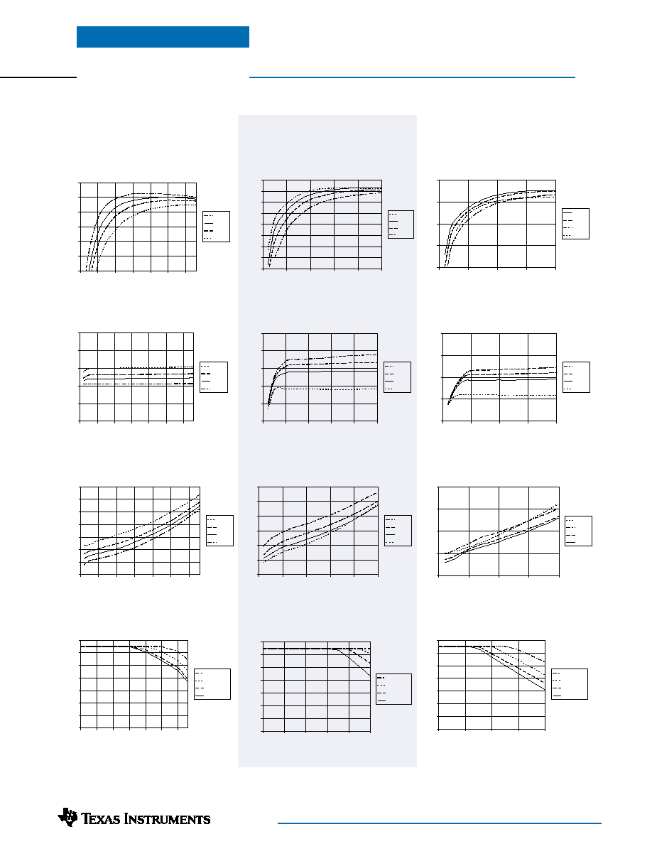
Note A:
All data listed in the above graphs has been developed from actual products tested at 25∞C. This data is considered typical data for the DC-DC Converter.
Note B:
SOA curves represent operating conditions at which internal components are at or below manufacturer's maximum rated operating temperature.
PT4562, 5.0 VDC
(See Note A)
Efficiency vs Output Current
Efficiency vs Output Current
Ripple vs Output Current
Ripple vs Output Current
Power Dissipation vs Output Current
Power Dissipation vs Output Current
PT4561, 3.3 VDC
(See Note A)
Safe Operating Area, V
in
=48V
(See Note B)
Safe Operating Area, V
in
=48V
(See Note B)
PT4560 Series
30-W 48-V Input
Isolated DC/DC Converter
PT4567, 1.8 VDC
(See Note A)
Typical Characteristics
Efficiency vs Output Current
Ripple vs Output Current
Power Dissipation vs Output Current
Safe Operating Area, V
in
=48V
(See Note B)
50
55
60
65
70
75
80
0
2
4
6
8
Iout (A)
Efficiency - %
36.0V
48.0V
60.0V
75.0V
V
IN
0
2
4
6
8
0
2
4
6
8
Iout (A)
Pd - Watts
75.0V
60.0V
48.0V
36.0V
V
IN
0
4
8
12
16
20
0
2
4
6
8
Iout (A)
Ripple - mV
75.0V
60.0V
48.0V
36.0V
V
IN
0
10
20
30
40
50
0
2
4
6
8
Iout (A)
Ripple - mV
75.0V
60.0V
48.0V
36.0V
V
IN
0
2
4
6
8
0
2
4
6
8
Iout (A)
Pd - Watts
75.0V
60.0V
36.0V
48.0V
V
IN
50
60
70
80
90
0
2
4
6
8
Iout (A)
Efficiency - %
48.0V
36.0V
60.0V
75.0V
V
IN
40
50
60
70
80
90
0
1
2
3
4
5
6
Iout (A)
Efficiency - %
48.0V
60.0V
36.0V
75.0V
V
IN
0
1
2
3
4
5
6
7
0
1
2
3
4
5
6
Iout (A)
Pd - Watts
75.0V
36.0V
60.0V
48.0V
V
IN
0
10
20
30
40
50
60
0
1
2
3
4
5
6
Iout (A)
Ripple - mV
75.0V
60.0V
48.0V
36.0V
V
IN
20
30
40
50
60
70
80
90
0.0
2.0
4.0
6.0
8.0
Iout (A)
Ambient Temperature (∞C)
200LFM
120LFM
60LFM
Nat Conv
Airflow
20
30
40
50
60
70
80
90
0
2
4
6
8
Iout (A)
Ambient Temperature (
∞
C)
200LFM
120LFM
60LFM
Nat conv
Airflow
20
30
40
50
60
70
80
90
0
1
2
3
4
5
6
Iout (A)
Ambient Temperature (
∞
C)
200LFM
120LFM
60LFM
Nat conv
Airflow
For technical support and more information, see inside back cover or visit www.ti.com
PT4560 Series
30-W 48-V Input
Isolated DC/DC Converter
PT4563, 12.0 VDC
(See Note A)
Efficiency vs Output Current
Ripple vs Output Current
Power Dissipation vs Output Current
Safe Operating Area, V
in
=48V
(See Note B)
PT4571, 9.0 VDC
(See Note A)
Note A:
All data listed in the above graphs has been developed from actual products tested at 25∞C. This data is considered typical data for the DC-DC Converter.
Note B:
SOA curves represent operating conditions at which internal components are at or below manufacturer's maximum rated operating temperature.
PT4564, 15 VDC
(See Note A)
Typical Characteristics
20
30
40
50
60
70
80
90
0.0
0.5
1.0
1.5
2.0
Iout (A)
Ambient Temperature (
∞
C)
200LFM
120LFM
60LFM
Nat Conv
Airflow
Efficiency vs Output Current
Ripple vs Output Current
Power Dissipation vs Output Current
Safe Operating Area, V
in
=48V
(See Note B)
Efficiency vs Output Current
Ripple vs Output Current
Power Dissipation vs Output Current
Safe Operating Area, V
in
=48V
(See Note B)
60
65
70
75
80
85
90
0
0.5
1
1.5
2
2.5
3
Iout (A)
Efficiency - %
36.0V
48.0V
60.0V
75.0V
V
IN
0
1
2
3
4
5
6
7
0
0.5
1
1.5
2
2.5
3
Iout (A)
Pd - Watts
75.0V
60.0V
48.0V
36.0V
V
IN
50
60
70
80
90
0
0.5
1
1.5
2
Iout (A)
Efficiency - %
48.0V
60.0V
75.0V
36.0V
V
IN
0
2
4
6
8
0
0.5
1
1.5
2
Iout (A)
Pd - Watts
36.0V
75.0V
60.0V
48.0V
V
IN
0
100
200
300
400
0
0.5
1
1.5
2
Iout (A)
Ripple - mV
75.0V
60.0V
48.0V
36.0V
V
IN
0
30
60
90
120
150
0
0.5
1
1.5
2
2.5
3
Iout (A)
Ripple - mV
75.0V
60.0V
48.0V
36.0V
V
IN
50
55
60
65
70
75
80
85
90
0
0.5
1
1.5
2
2.5
Iout (A)
Efficiency - %
36.0V
48.0V
60.0V
75.0V
V
IN
0
1
2
3
4
5
6
0
0.5
1
1.5
2
2.5
Iout (A)
Pd - Watts
75.0V
60.0V
48.0V
36.0V
V
IN
0
40
80
120
160
200
0
0.5
1
1.5
2
2.5
Iout (A)
Ripple - mV
75.0V
60.0V
48.0V
36.0V
V
IN
20
30
40
50
60
70
80
90
0
0.5
1
1.5
2
2.5
Iout (A)
Ambient Temperature (
∞
C)
200LFM
120LFM
60LFM
Nat conv
Airflow
20
30
40
50
60
70
80
90
0.0
0.5
1.0
1.5
2.0
2.5
3.0
Iout (A)
Ambient Temperature (
∞
C)
200LFM
120LFM
60LFM
Nat Conv
Airflow
Application Notes
For technical support and more information, see inside back cover or visit www.ti.com
Adjusting the Output Voltage of Power Trends'
30W Isolated DC/DC Converter Series
The factory pre-set output voltage of Power Trends' 30W
series of isolated DC/DC converters may be adjusted
within a nominal ±10% range. This is accomplished with
the addition of a single external resistor. For the input
voltage range specified in the data sheet, Table 1 gives the
allowable adjustment range for each model as V
o
(min)
and V
o
(max).
Adjust Up:
An increase in the output voltage is obtained
by adding a resistor, R
2
between V
o
adjust (pin 18), and
-Remote Sense (pin 13). See note 4.
Adjust Down:
Add a resistor
(R
1
)
, between V
o
adjust (pin
18), and +Remote Sense (pin 19).
Refer to Figure 1 and Tables 2 & 3 for both the placement and
value of the required resistor,
(R
1
)
or R
2
.
Notes:
1. Use only a single 1% resistor in either the
(R
1
)
or R
2
location. Place the resistor as close to the ISR as possible.
2. Never connect capacitors to V
o
adjust. Any capacitance
added to the V
o
adjust control pin will affect the stability of
the ISR.
Table 1
DC/DC CONVERTER ADJUSTMENT RANGE AND FORMULA PARAMETERS
Series Pt #
AL Case:
24V Bus
PT3341
PT3342
PT3343
PT3344
48V Bus
PT3327
PT3325
PT3326
PT3321
PT3322
PT3323
PT3324
CU Case:
24V Bus
PT4585
PT4581
PT4582
PT4583
PT4584
48V Bus
PT4567
PT4565
PT4566
PT4561
PT4562
PT4571
PT4563
PT4564
V
o
(nom)
1.8V
1.8V
2.0V
2.5V
3.3V
5.0V
9.0V
12.0V
15.0V
Vo(min)
1.62V
1.62V
1.8V
2.25V
2.95V
4.5V
7.0V
10.8V
13.5V
Vo(max)
2.5V
1.98V
2.2V
2.75V
3.65V
5.5V
10.0V
13.2V
16.5V
V
r
1.225V
1.225V
1.225V
1.225V
1.225V
1.225V
2.5V
2.5V
2.5V
K
o
(V∑k
)
69.58
69.58
62.47
42.33
68.89
68.71
133.25
135.9
137.5
R
s
(k
)
80.6
80.6
150.0
121.0
150.0
121.0
110
90.9
80.6
Figure 1
( R 1 )
A d j D o w n
R 2
Adj
U p
C i n
1 0 0
µ
F
1 0 0 V
(Optional)
+
C o u t
3 3 0
µ
F
+
L
O
A
D
+ V
out
-V
out
+ V
in
-V
in
3 0 W I s o l a t e d
1 8
4, 5, 6
7, 8, 9
+Vin
+Vout
-Vin
Vo(adj)
R e m o t e
On/Off
2
Sns(+)
1 9
10 - 12
-Vout
14 - 17
Sns(-)
1 3
3. If the remote sense pins are not being used, the resistors
(R1)
and R2 can be connected to +V
out
or -V
out
respectively.
4. The adjusted output voltage, V
a
effectively sets the voltage
across pins 13 and 19 (±Remote Sense). When using the
remote sense pins, V
out
(measured directly across pins 10≠
12, and 14≠17) can be significantly higher than V
a
, and may
exceed V
o
(max). If V
a
is adjusted upward of V
o
(max), the
the minimum input voltage is increased by the same
percentage as V
out
exceeds V
o
(max).
The values of
(R
1
)
[adjust down], and R
2
[adjust up], can
also be calculated using the following formulas.
(R
1
)
=
K
o
(V
a
≠ V
r
)
≠ R
s
k
V
r
(V
o
≠ V
a
)
R
2
=
K
o
≠ R
s
k
(V
a
≠ V
o
)
Where
V
o
= Original output voltage
V
a
= Adjusted output voltage
V
r
= Reference voltage (Table 1)
K
o
= Multiplier constant (Table 1)
R
s
= Series resistance (Table 1)
PT3320/3340/4560/4580 Series