 | ÐлекÑÑоннÑй компоненÑ: PT4685 | СкаÑаÑÑ:  PDF PDF  ZIP ZIP |
Äîêóìåíòàöèÿ è îïèñàíèÿ www.docs.chipfind.ru
For technical support and more information, see inside back cover or visit www.ti.com
Description
The PT4680 ExcaliburTM Series
is a dual-output isolated DC/DC
converter that combine state-of-the-
art power conversion technology with
unparalleled flexibility. Operating
from a (24V) industry standard input
bus, the PT4680 series provides up to
20 ADC of output current from two
independently regulated voltages
(each output 15 ADC max).
The PT4680 series is characterized
with high efficiencies and ultra-fast
transient response, and incorporates
many features to facilitate system
integration. These include a flexible
"On/Off" enable control, output
Features
·
Dual Outputs
(Independently Regulated)
·
Power-up/Down Sequencing
·
Input Voltage Range:
18V to 36V
·
1500 VDC Isolation
·
Temp Range: 40° to 100°C
·
High Efficiency: 88%
·
Fixed Frequency Operation
·
Over-Current Protection
(Both Outputs)
Ordering Information
Pt. No.
Vo
1
/Vo
2
PT4681
o
= 5.0/3.3 Volts
PT4682
o
= 3.3/2.5 Volts
PT4683
o
= 3.3/1.8 Volts
PT4685
o
= 3.3/1.5 Volts
PT4686
o
= 2.5/1.8 Volts
PT4687
o
= 5.0/1.8 Volts
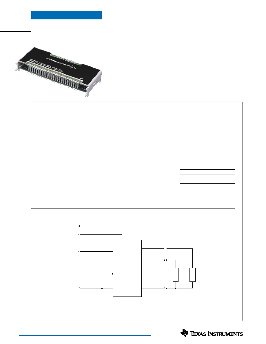
Typical Application
PT4680
+Vin
EN 1*
EN 2
Vin
Vo
1
adj
Vo
2
adj
Vo
1
Vo
2
C O M
912
2124
1419
L
O
A
D
L
O
A
D
V o
1
V o
2
V
1
Adjust
V
2
Adjust
+ V
IN
V
IN
20
13
1
4
3
2
C O M
* Inverted logic
·
Dual Logic On/Off Control
·
Over-Temperature Shutdown
·
Over-Voltage Protection
(Coordinated Shutdown)
·
Under-Voltage Lockout
·
Input Differential EMI Filter
·
Solderable Copper Case
·
Safety Approvals (Pending):
UL 60950
CSA 22.2 60950
current limit, over-temperature pro-
tection, and an input under-voltage
lock-out. In addition, both output
voltages are designed to meet the
power-up/power -down sequencing
requirements of popular DSP ICs.
The PT4680 series is housed in
space-saving solderable copper case.
The package does not require a
heatsink and is available in both
vertical and horizontal configura-
tions, including surface mount. The
`N' configuration occupies less than 2
in² of PCB area.
PT Series Suffix
(PT1234
x
)
Case/Pin
Order
Package
Configuration
Suffix
Code
Vertical
N
(EKD)
Horizontal
A
(EKA)
SMD
C
(EKC)
(Reference the applicable package code draw-
ing for the dimensions and PC board layout)
PT4680 Series
20-A 24-V Input Dual Output
Isolated DC/DC Converter
SLTS141A
(Revised 1/28/2002)

For technical support and more information, see inside back cover or visit www.ti.com
Pin Descriptions
+Vin:
The positive input supply for the module with
respect to V
in
. If powering the module from a -24V
telecom central office supply, this input is connected
to the primary system ground.
Vin:
The negative input supply for the module, and
the 0VDC reference for the EN 1, EN 2, TEMP, and
AUX signals. When the module is powered from a
+24V supply, this input is connected to the 24V Return.
EN 1:
The negative logic input that enables the
module output. This pin is TTL compatible and
referenced to V
in
. A logic `0' at this pin enables the
module's outputs. A logic `1' or high impedance
disables the module's outputs. If not used, the pin
must be connected to V
in
.
EN 2:
The positive logic input that enables the
module output. This pin is TTL compatible and
referenced to V
in
. A logic `1' or high impedance
enables the module's outputs. If not used, the pin
should be left open circuit.
TEMP:
This pin produces an output signal that tracks
the module's metal case temperature. The output
voltage is referenced to V
in
and rises approximately
10mV/°C from an intital value of 0.1VDC at -40°C
(V
Temp
=0.5 + 0.01·T
Case
). The signal is available
whenever the module is supplied with a valid input
voltage, and is independant of the enable logic status.
(
Note:
A load impedance of less than 1M
will adversly
affect the module's over-temperature shutdown threshold.
Use a high-impedance input when monitoring this
signal.)
AUX:
Produces a regulated output voltage of 11.6V
±5%, which is referenced to V
in
. The current drawn
from the pin must be limited to 10mA. The voltage
may be used to indicate the output status of the
module to a primary referenced circuit, or power a
low-current amplifer.
Vo
1
:
The higher regulated output voltage, which is
referenced to the COM node.
Vo
2
:
The lower regulated output voltage, which is
referenced to the COM node.
COM:
The secondary return reference for the module's
two regulated output voltages. It is DC isolated from
the input supply pins.
Vo
1
Adjust:
Using a single resistor, this pin allows Vo
1
to be adjusted higher or lower than the preset value.
If not used, this pin should be left open circuit.
Vo
2
Adjust:
Using a single resistor, this pin allows Vo
2
to be adjusted higher or lower than the preset value.
If not used, this pin should be left open circuit.
On/Off Logic
Pin 3
Pin 4
Output Status
1
×
Off
0
1
On
×
0
Off
Pin-Out Information
Pin
Function
1
+Vin
2
-Vin
3
EN 1
4
EN 2
5
TEMP
6
AUX
7
Do Not Connect
8
Do Not Connect
9
+Vo
1
Pin
Function
10
+Vo
1
11
+Vo
1
12
+Vo
1
13
Vo
1
Adjust
14
COM
15
COM
16
COM
17
COM
18
COM
Notes:
Logic 1 =Open collector
Logic 0 = Vin (pin 2) potential
For positive Enable function, connect pin 3
to pin 2 and use pin 4.
For negative Enable function, leave pin 4
open and use pin 3.
Note: Shaded functions indicate signals that are
referenced to the input (-Vin) potential.
Pin
Function
19
COM
20
Vo
2
Adjust
21
+Vo
2
22
+Vo
2
23
+Vo
2
24
+Vo
2
25
Do Not Connect
26
Do Not Connect
PT4680 Series
20-A 24-V Input Dual Output
Isolated DC/DC Converter

For technical support and more information, see inside back cover or visit www.ti.com
Specifications
(Unless otherwise stated, T
a
=25°C, V
in
=24V, & Io
1
=Io
2
=10A)
PT4680 SERIES
Characteristics
Symbols
Conditions
Min
Typ
Max
Units
Output Current
Io
1
Vo
1
0
--
15
A
Io
2
Vo
2
0
--
15
Io
1
+Io
2
Total (both outputs)
0
--
20
(1)
A
Input Voltage Range
V
in
18
24
36
V
Set Point Voltage Tolerance
V
o
tol
--
±1
±2
%V
o
Temperature Variation
Reg
temp
40 to +100°C Case, Io
1
=Io
2
=0A
--
±0.5
--
%V
o
Line Regulation
Reg
line
Over V
in
range with Io
1
=Io
2
=5A
--
±5
±10
mV
Load Regulation
Reg
load
1A
Io
1
15A, Io
2
=1A
Vo
1
--
±2
±10
mV
1A
Io
2
15A, Io
1
=1A
Vo
2
--
±2
±10
Cross Regulation
Reg
cross
1A
Io
2
15A, Io
1
=1A
Vo
1
--
±2
±10
mV
1A
Io
1
15A, Io
2
=1A
Vo
2
--
±2
±5
Total Output Variation
V
o
tol
Includes set-point, line load,
Vo
1
--
±2
±3
%V
o
40°C to +100°C case
Vo
2
--
±2
±3
Efficiency
Io
1
=1o
2
=10A
PT4681
--
88
--
PT4682
--
87
--
PT4683
--
87
--
PT4685
--
86
--
%
PT4686
--
85
--
PT4687
--
86
--
V
o
Ripple (pk-pk)
V
r
Io
1
=Io
2
=5A, 20MHz bandwidth
V
o
=5V
--
--
75
mV
pp
V
o
<5V
--
--
50
Transient Response
t
tr
1A/µs load step from 50% to 100% I
o
max
--
25
100
µSec
(either output)
--
6.0
--
%V
o
Current Limit
I
lim
Each output with other unloaded
15.5
18
--
A
Output Rise Time
V
on
At turn-on to within 90% of V
o
--
5
10
mSec
Output Over-Voltage Protection
OVP
Either output; shutdown and latch off
--
125
(2)
--
%V
o
Switching Frequency
f
s
280
--
320
kHz
Under-Voltage-Lockout
UVLO
Rising
--
17
18
V
Falling
15
16
--
Internal Input Capacitance
C
in
--
2
--
µF
On/Off Control
Referenced to V
in
Input High Voltage
V
IH
3.5
--
--
V
Input Low Voltage
V
IL
0
--
0.8
(3)
Input Low Current
I
IL
--
0.5
--
mA
Quiescent Current
I
in
standby
Pins 2, 3, & 4 connected
--
3
5
mA
External Output Capacitance
C
out
Per each output
0
--
5,000
µF
Primary/Secondary Isolation
V
iso
1500
--
--
V
C
iso
--
1500
--
pF
R
iso
10
--
--
M
Temperature Sense
V
temp
Output voltage at temperatures:-
40°C
--
0.1
(4)
--
V
100°C
--
1.5
(4)
--
Over-Temperature Shutdown
OTP
Case temperature (auto restart)
--
110
--
°C
Operating Temperature Range
T
a
Over V
in
range
40
--
+85
(5)
°C
Storage Temperature
T
s
--
40
--
+125
°C
Mechanical Shock
--
Per Mil-STD-883D, Method 2002.3
--
500
--
G's
Mechanical Vibration
--
Vertical
--
10
(6)
--
G's
Per Mil-STD-883D, 202,000Hz
Horizontal
--
20
(6)
--
Weight
--
--
--
90
--
grams
Flammability
--
Materials meet UL 94V-0
Notes: (1) The sum-total current from Vo
1
& Vo
2
must not exceed 20ADC.
(2) This is a fixed parameter. Adjusting Vo
1
or Vo
2
higher will increase the module's sensitivity to over-voltage detection. For more information, see the
application note on output voltage adjustment.
(3) The EN
1
and EN
2
control inputs (pins 3 & 4) have internal pull-ups and may be controlled with an open-collector (or open-drain) transistor. Both
inputs are diode protected and can be connected to +V
in
. The maximum open-circuit voltage is 5.4V.
(4) Voltage output at "TEMP" pin is defined by the equation:- V
TEMP
= 0.5 + 0.01·T, where T is in °C. See pin descriptions for more information.
(5) See SOA curves or consult the factory for the appropriate derating.
(6) The case pins on the through-holed package types (suffixes N & A) must be soldered. For more information see the applicable package outline drawing.
PT4680 Series
20-A 24-V Input Dual Output
Isolated DC/DC Converter
For technical support and more information, see inside back cover or visit www.ti.com
Note A:
All Characteristic data in the above graphs has been developed from actual products tested at 25°C. This data is considered typical data for the converter.
Note B:
SOA curves represent operating conditions at which internal components are at or below manufacturer's maximum rated operating temperatures.
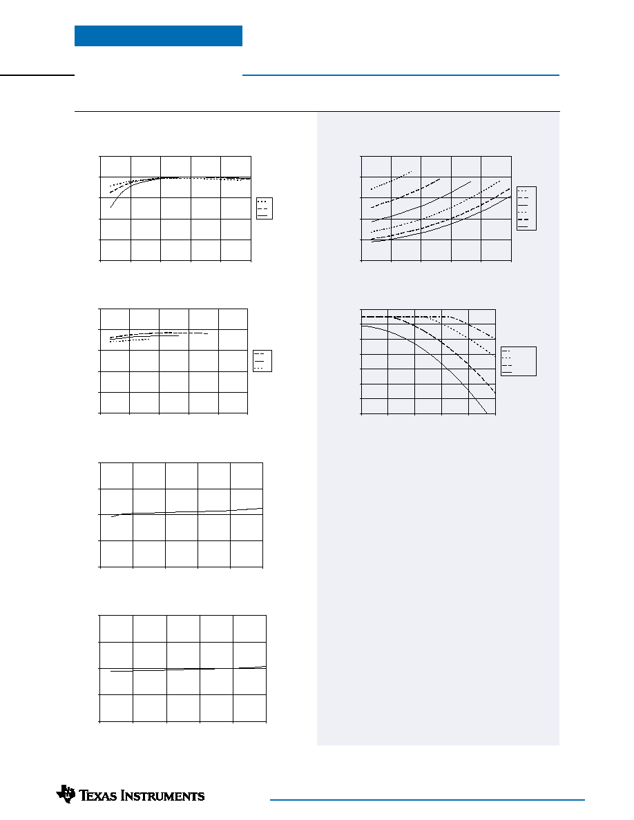
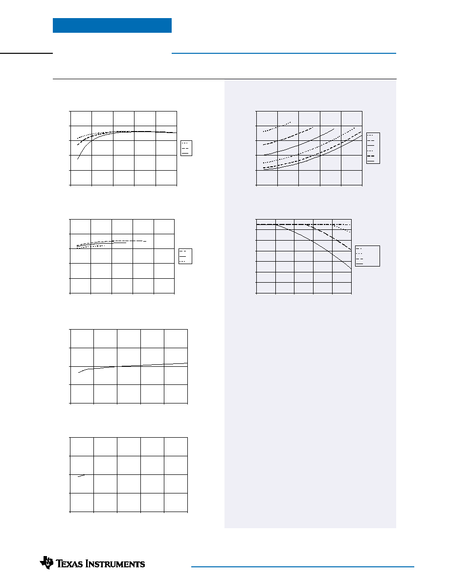
Typical Characteristics
PT4681 (Vo
1
/Vo
2
=5.0V/3.3V); V
in
=24V
(See Notes A & B)
Efficiency vs Io
1
; Io
2
@1A, 3A, and 6A
Power Dissipation vs Io
1
and Io
2
Cross Regulation: Vo
1
vs Io
2
@Io
1
=1A
Cross Regulation: Vo
2
vs Io
1
@Io
2
=1A
Efficiency vs Io
1
; Io
2
@9A, 12A, and 15A
Safe Operating Area: (Io
1
+ Io
2
)
PT4681--24V
20-A 24-V Input Dual Output
Isolated DC/DC Converter
4.95
4.975
5
5.025
5.05
0
3
6
9
12
15
I
2
out (A)
V
1
out (V)
3.28
3.29
3.3
3.31
3.32
0
3
6
9
12
15
I
1
out (A)
V
2
out (V)
0
3
6
9
12
15
0
3
6
9
12
15
I
1
out (A)
Pd - Watts
15
12
9
6
3
1
I
2
out
50
60
70
80
90
100
0
3
6
9
12
15
I
1
out (A)
Efficiency - %
6
3
1
I
2
out
50
60
70
80
90
100
0
3
6
9
12
15
I
1
out (A)
Efficiency - %
9
12
15
I
2
out
20
30
40
50
60
70
80
90
5
8
11
14
17
20
Io
1
+ Io
2
(A)
Ambient Temperature (°C)
300LFM
200LFM
100LFM
Nat conv
Airflow
For technical support and more information, see inside back cover or visit www.ti.com
Note A:
All Characteristic data in the above graphs has been developed from actual products tested at 25°C. This data is considered typical data for the converter.
Note B:
SOA curves represent operating conditions at which internal components are at or below manufacturer's maximum rated operating temperatures.
PT4682 (Vo
1
/Vo
2
=3.3V/2.5V); V
in
=24V
(See Notes A & B)
Efficiency vs Io
1
; Io
2
@1A, 3A, and 6A
Power Dissipation vs Io
1
and Io
2
Cross Regulation: Vo
1
vs Io
2
@I
1
out =1A
Cross Regulation: Vo
2
vs Io
1
@Io
2
=1A
Efficiency vs Io
1
; Io
2
@9A, 12A, and 15A
Safe Operating Area: (Io
1
+ Io
2
)
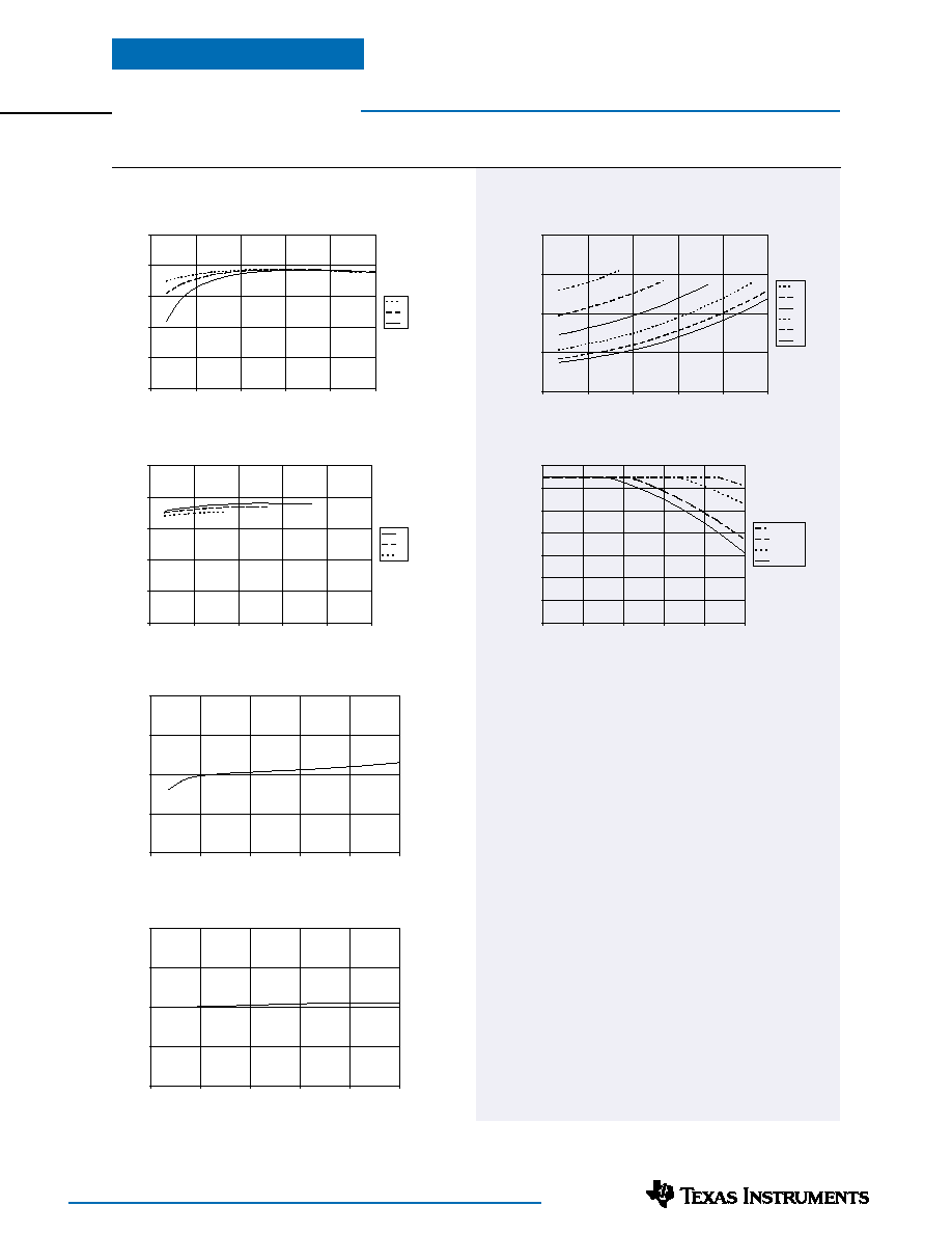
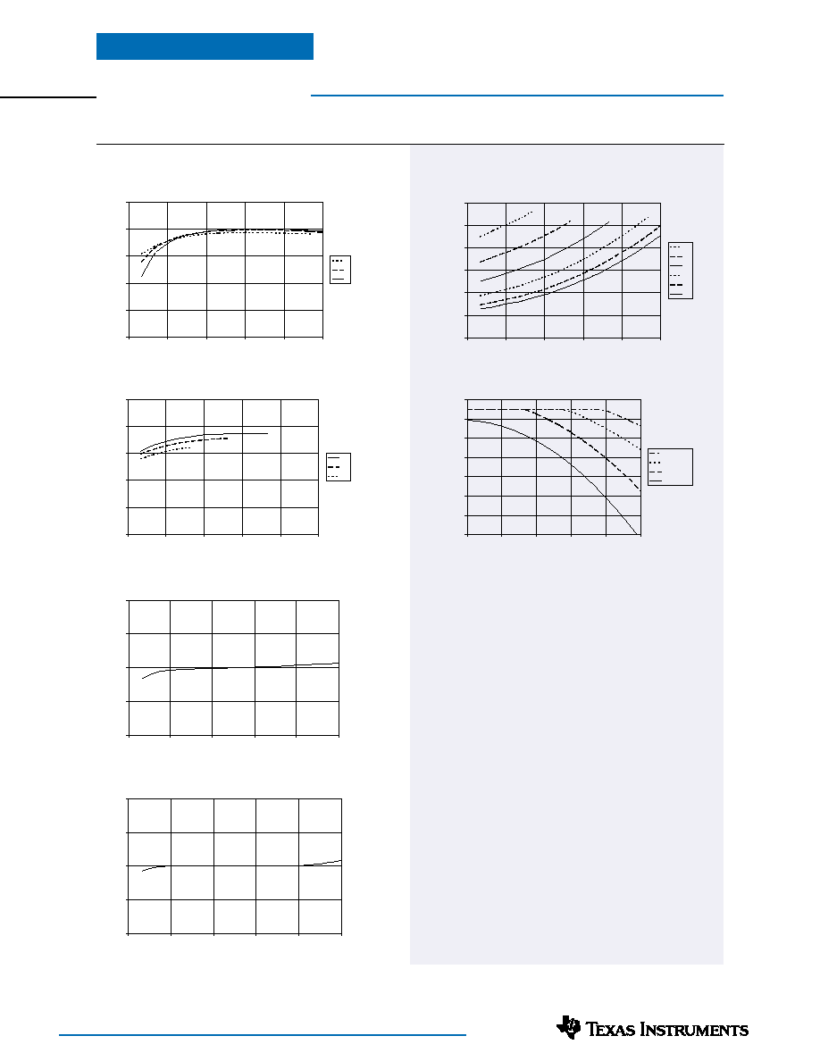
Typical Characteristics
PT4682--24V
20-A 24-V Input Dual Output
Isolated DC/DC Converter
50
60
70
80
90
100
0
3
6
9
12
15
I
1
out (A)
Efficiency - %
6
3
1
I
2
out
50
60
70
80
90
100
0
3
6
9
12
15
I
1
out (A)
Efficiency - %
9
12
15
I
2
out
3.28
3.29
3.3
3.31
3.32
0
3
6
9
12
15
I
2
out (A)
V
1
out (V)
2.48
2.49
2.5
2.51
2.52
0
3
6
9
12
15
I
1
out (A)
V
2
out (V)
0
3
6
9
12
0
3
6
9
12
15
I
1
out (A)
Pd - Watts
15
12
9
6
3
1
I
2
out
20
30
40
50
60
70
80
90
5
8
11
14
17
20
Io
1
+ Io
2
(A)
Ambient Temperature (
°
C)
300LFM
100LFM
200LFM
Nat conv
Airflow
For technical support and more information, see inside back cover or visit www.ti.com
Note A:
All Characteristic data in the above graphs has been developed from actual products tested at 25°C. This data is considered typical data for the converter.
Note B:
SOA curves represent operating conditions at which internal components are at or below manufacturer's maximum rated operating temperatures.
Typical Characteristics
PT4683 (Vo
1
/Vo
2
=3.3V/1.8V); V
in
=24V
(See Notes A & B)
Efficiency vs Io
1
; Io
2
@1A, 3A, and 6A
Power Dissipation vs Io
1
and Io
2
Cross Regulation: Vo
1
vs Io
2
@Io
1
=1A
Cross Regulation: Vo
2
vs Io
1
@Io
2
=1A
Efficiency vs Io
1
; Io
2
@9A, 12A, and 15A
Safe Operating Area: (Io
1
+ Io
2
)
PT4683--24V
20-A 24-V Input Dual Output
Isolated DC/DC Converter
50
60
70
80
90
100
0
3
6
9
12
15
I
1
out (A)
Efficiency - %
6
3
1
I
2
out
50
60
70
80
90
100
0
3
6
9
12
15
I
1
out (A)
Efficiency - %
9
12
15
I
2
out
3.28
3.29
3.3
3.31
3.32
0
3
6
9
12
15
I
2
out (A)
V
1
out (V)
0
2
4
6
8
10
0
3
6
9
12
15
I
1
out (A)
Pd - Watts
15
12
9
6
3
1
I
2
out
1.78
1.79
1.8
1.81
1.82
0
3
6
9
12
15
I
1
out (A)
V
2
out (V)
20
30
40
50
60
70
80
90
5
8
11
14
17
20
Io
1
+ Io
2
(A)
Ambient Temperature (
°
C)
200LFM
100LFM
Nat conv
Airflow

For technical support and more information, see inside back cover or visit www.ti.com
Efficiency vs Io
1
; Io
2
@1A, 3A, and 6A
Power Dissipation vs Io
1
and Io
2
Cross Regulation: Vo
1
vs Io
2
@Io
1
=1A
Cross Regulation: Vo
2
vs Io
1
@Io
2
=1A
Efficiency vs Io
1
; Io
2
@9A, 12A, and 15A
Safe Operating Area: (Io
1
+ Io
2
)
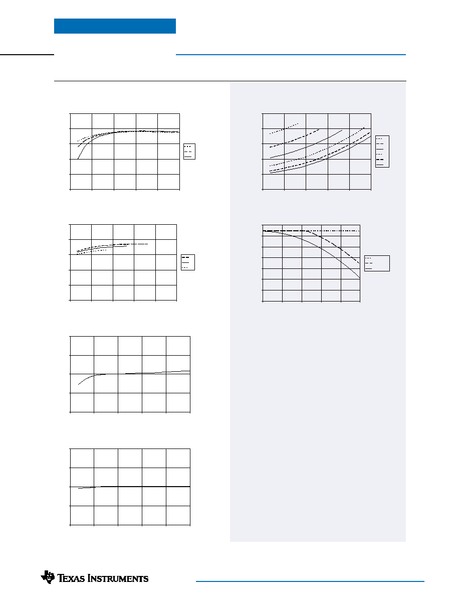
Typical Characteristics
PT4685 (Vo
1
/Vo
2
=3.3V/1.5V); V
in
=24V
Note A:
All Characteristic data in the above graphs has been developed from actual products tested at 25°C. This data is considered typical data for the converter.
Note B:
SOA curves represent operating conditions at which internal components are at or below manufacturer's maximum rated operating temperatures.
PT4685--24V
20-A 24-V Input Dual Output
Isolated DC/DC Converter
50
60
70
80
90
100
0
3
6
9
12
15
I
1
out (A)
Efficiency - %
6
3
1
I
2
out
50
60
70
80
90
100
0
3
6
9
12
15
I
1
out (A)
Efficiency - %
9
12
15
I
2
out
3.28
3.29
3.3
3.31
3.32
0
3
6
9
12
15
I
2
out (A)
V
1
out (V)
0
2
4
6
8
10
0
3
6
9
12
15
I
1
out (A)
Pd - Watts
15
12
9
6
3
1
I
2
out
1.48
1.49
1.5
1.51
1.52
0
3
6
9
12
15
I
1
out (A)
V
2
out (V)
20
30
40
50
60
70
80
90
5
8
11
14
17
20
Io
1
+ Io
2
(A)
Ambient Temperature (
°
C)
200LFM
100LFM
Nat conv
Airflow
For technical support and more information, see inside back cover or visit www.ti.com
Note A:
All Characteristic data in the above graphs has been developed from actual products tested at 25°C. This data is considered typical data for the converter.
Note B:
SOA curves represent operating conditions at which internal components are at or below manufacturer's maximum rated operating temperatures.
PT4686 (Vo
1
/Vo
2
=2.5V/1.8V); V
in
=24V
Typical Characteristics
Efficiency vs Io
1
; Io
2
@1A, 3A, and 6A
Power Dissipation vs Io
1
and Io
2
Cross Regulation: Vo
1
vs Io
2
@Io
1
=1A
Cross Regulation: Vo
2
vs Io
1
@Io
2
=1A
Efficiency vs Io
1
; Io
2
@9A, 12A, and 15A
Safe Operating Area: (Io
1
+ Io
2
)
PT4686--24V
20-A 24-V Input Dual Output
Isolated DC/DC Converter
50
60
70
80
90
100
0
3
6
9
12
15
I
1
out (A)
Efficiency - %
6
3
1
I
2
out
50
60
70
80
90
100
0
3
6
9
12
15
I
1
out (A)
Efficiency - %
9
12
15
I
2
out
2.48
2.49
2.5
2.51
2.52
0
3
6
9
12
15
I
2
out (A)
V
1
out (V)
0
2
4
6
8
10
0
3
6
9
12
15
I
1
out (A)
Pd - Watts
15
12
9
6
3
1
I
2
out
1.78
1.79
1.8
1.81
1.82
0
3
6
9
12
15
I
1
out (A)
V
2
out (V)
20
30
40
50
60
70
80
90
5
8
11
14
17
20
Io
1
+ Io
2
(A)
Ambient Temperature (
°
C)
300LFM
200LFM
100LFM
Nat conv
Airflow
For technical support and more information, see inside back cover or visit www.ti.com
Efficiency vs Io
1
; Io
2
@1A, 3A, and 6A
Power Dissipation vs Io
1
and Io
2
Cross Regulation: Vo
1
vs Io
2
@Io
1
=1A
Cross Regulation: Vo
2
vs Io
1
@Io
2
=1A
Efficiency vs Io
1
; Io
2
@9A, 12A, and 15A
Safe Operating Area: (Io
1
+ Io
2
)
Typical Characteristics
PT4687 (Vo
1
/Vo
2
=5V/1.8V); V
in
=24V
Note A:
All Characteristic data in the above graphs has been developed from actual products tested at 25°C. This data is considered typical data for the converter.
Note B:
SOA curves represent operating conditions at which internal components are at or below manufacturer's maximum rated operating temperatures.
PT4687--24V
20-A 24-V Input Dual Output
Isolated DC/DC Converter
50
60
70
80
90
100
0
3
6
9
12
15
I
1
out (A)
Efficiency - %
9
12
15
I
2
out
1.78
1.79
1.8
1.81
1.82
0
3
6
9
12
15
I
1
out (A)
V
2
out (V)
0
2
4
6
8
10
12
0
3
6
9
12
15
I
1
out (A)
Pd - Watts
15
12
9
6
3
1
I
2
out
4.95
4.975
5
5.025
5.05
0
3
6
9
12
15
I
2
out (A)
V
1
out (V)
50
60
70
80
90
100
0
3
6
9
12
15
I
1
out (A)
Efficiency - %
6
3
1
I
2
out
20
30
40
50
60
70
80
90
5
8
11
14
17
20
Io
1
+ Io
2
(A)
Ambient Temperature (
°
C)
300LFM
200LFM
100LFM
Nat conv
Airflow

Application Notes
For technical support and more information, see inside back cover or visit www.ti.com
PT4660 & PT4680 Series
Operating Features & System Considerations for the
PT4660/PT4680 Dual-Output DC/DC Converters
Over-Current Protection
The dual-outputs of the PT4660 and PT4680 series of
DC/DC converters have independent output voltage
regulation and current limit control. Applying a load
current in excess of the current limit threshold at either
output will cause the respective output voltage to drop.
However, the voltage at Vo
2
is derived from Vo
1
. There-
fore a current limit fault on Vo
1
will also cause Vo
2
to
drop. Conversely, a current limit fault applied to Vo
2
will only cause Vo
2
voltage to drop, and Vo
1
will remain
in regulation.
The current limit circuitry incorporates a limited amount
of foldback. The fault current flowing into an absolute
short circuit is therefore slightly less than the current
limit threshold. Recovery from a current limit fault is
automatic and the converter will not be damaged by a
continuous short circuit at either output.
Output Over-Voltage Protection
Each output is monitored for over voltage (OV). For fail
safe operation and redundancy, the OV fault detection
circuitry uses a separate reference to the voltage regulation
circuits. The OV threshold is fixed, and set nominally 25%
higher than the set-point output voltage. If either output
exceeds the threshold, the converter is shutdown and
must be actively reset. The OV protection circuit can be
reset by momentarily turning the converter off. This is
accomplished by either cycling one of the output enable
control pins (EN1 or EN2), or by removing the input
power to the converter. Note: If Vo
1
or Vo
2
is adjusted to a
higher voltage, the margin between the respective steady-state
output voltage and its OV threshold is reduced. This can make
the module sensitive to OV fault detection, that may result
from random noise and load transients.
Over-Temperature Protection
The PT4660/80 DC/DC converters have an internal
temperature sensor, which monitors the temperature of
the module's metal case. If the case temperature exceeds
a nominal 115°C the converter will shut down. The
converter will automatically restart when the sensed
temperature returns to about 100°C. The analog voltage
generated by the sensor is also made available at the
`TEMP' output (pin 5), and can be monitored by the host
system for diagnostic purposes. Consult the `Pin Descrip-
tions' section of the data sheet for further information on
this feature.
Under-Voltage Lock-Out
The Under-Voltage Lock-Out (UVLO) circuit prevents
operation of the converter whenever the input voltage to
the module is insufficient to maintain output regulation.
The UVLO has approximately 2V of hysterisis. This is
to prevent oscillation with a slowly changing input voltage.
Below the UVLO threshold the module is off and the
enable control inputs, EN1 and EN2 are inoperative.
Primary-Secondary Isolation
The PT4460/80 series of DC/DC converters incorporate
electrical isolation between the input terminals (primary)
and the output terminals (secondary). All converters are
production tested to a withstand voltage of 1500VDC.
The isolation complies with UL60950 and EN60950,
and the requirements for operational isolation. This
allows the converter to be configured for either a positive
or negative input voltage source.
The regulation control circuitry for these modules is
located on the secondary (output) side of the isolation
barrier. Control signals are passed between the primary
and secondary sides of the converter via a proprietory
magnetic coupling scheme. This eliminates the use of
opto-couplers. The data sheet `Pin Descriptions' and
`Pin-Out Information' provides guidance as to which
reference (primary or secondary) that must be used for
each of the external control signals.
Fuse Recommendations
If desired an input fuse may be added to protect against
the application of a reverse input voltage.
For technical support and more information, see inside back cover or visit www.ti.com
Application Notes
0
5
10
15
20
25
30
35
t (milliseconds)
Vo
1
(2V/Div)
Vo
2
(2V/Div)
I
IN
(0.5A/Div)
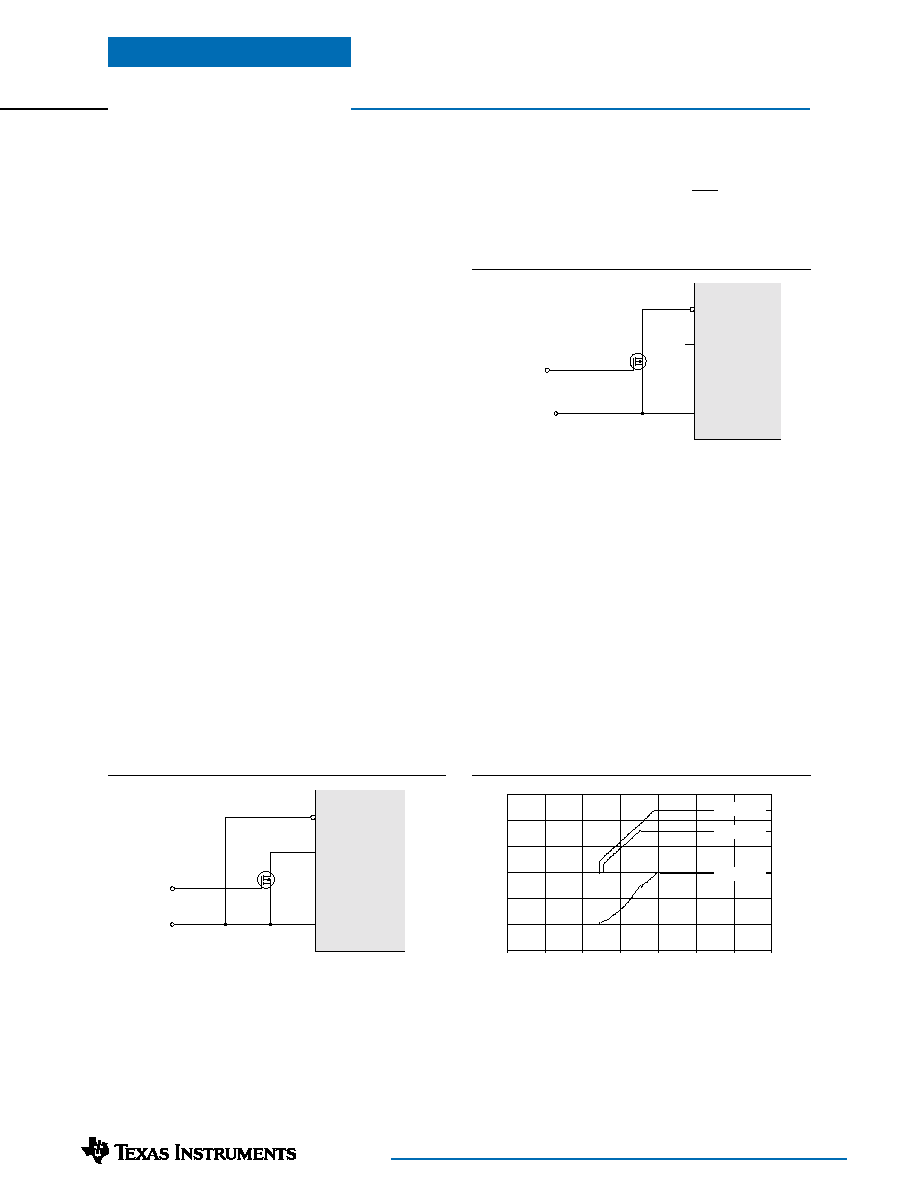
Figure 3; Vo
1
, Vo
2
Power-Up Sequence
PT4660 & PT4680 Series
On/Off Output Voltage Sequencing
The output voltages from the PT4660 series of DC/
DC converters are independantly regulated, and are
internally sequenced to meet the power-up requirements
of popular microprocessor and DSP chipsets. Figure 3
shows the waveforms from a PT4661 after the converter
is enabled at t=0s. During power-up, the Vo
1
and Vo
2
voltage waveforms typically track within 0.4V prior to
Vo
2
reaching regulation. The waveforms were measured
with a 5-Adc resistive load at each output, and with a 48-
VDC input source applied. The converter typically
produces a fully regulated output within 25ms. The
actual turn-on time will vary slightly with input voltage,
but the power-up sequence is independent of the load at
either output.
Using the On/Off Enable Controls on the PT4660
and PT4680 Series of DC/DC Converters
The PT4660 (48V input) and PT4680 (24V input) series
of 75-W dual-output DC/DC converters incorporates
both positive and negative logic Output Enable controls.
EN1 (pin 3) is the positive enable input, and EN2 (pin 4)
is the negative enable input. Both inputs are TTL logic
compatible, and are electrically referenced to -V
in
(pin 2)
on the primary (input) side of the converter. A pull-up
resistor is not required, but may be added if desired.
Adding a pull-up resistor from either input, up to +V
in
,
will not damage the converter.
Automatic (UVLO) Power-Up
Connecting EN1 (pin 3) to -V
in
(pin 2) and leaving EN2
(pin 4) open-circuit configures the converter for auto-
matic power up. (See data sheet "Typical Application").
The converter control circuitry incorporates an "Under
Voltage Lockout" (UVLO) function, which disables the
converter until the minimum specified input voltage is
present at ±V
in
. (See data sheet Specifications). The UVLO
circuitry ensures a clean transition during power-up and
power-down, allowing the converter to tolerate a slow-
rising input voltage. For most applications EN1 and
EN2, can be configured for automatic power-up.
Positive Output Enable (Negative Inhibit)
To configure the converter for a positive enable function,
connect EN1 (pin 3) to -V
in
(pin 2), and apply the system
On/Off control signal to EN2 (pin 4). In this configura-
tion, a logic `0' (-V
in
potential) applied to pin 4 disables
the converter outputs. An example of this configuration is
detailed in Figure 1.
Negative Output Enable (Positive Inhibit)
To configure the converter for a negative enable function,
EN2 (pin 4) is left open circuit, and the system On/Off
control signal is applied to EN1 (pin 3). A logic `0' (-V
in
potential) must then be applied to pin 3 in order to
PT4660
EN 1*
EN 2
Vin
V
I N
1 = O u t p u t s O f f
4
3
2
BSS138
P T 4 6 6 0
EN 1*
EN 2
Vin
V
IN
4
3
2
1 = O u t p u t s O n
BSS138
Figure 2; Negative Enable Configuration
Figure 1; Positive Enable Configuration
During turn-off, both outputs drop rapidly due to the
discharging effect of actively switched rectifiers. The
voltage at Vo
1
remains higher than Vo
2
during this pe-
riod. The discharge time is typically 100µs, but will vary
with the amount of external load capacitance.
enable the outputs of the converter. An example of this
configuration is detailed in Figure 2. Note: The converter
will only produce and output voltage if a valid input voltage is
applied to ±V
in
.
Application Notes
For technical support and more information, see inside back cover or visit www.ti.com
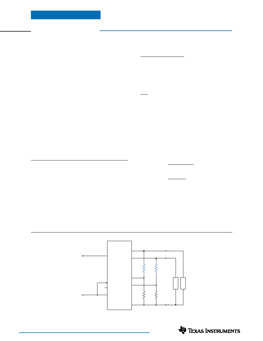
Adjusting the Output Voltage of the PT4660 and
PT4680 Dual Output Voltage DC/DC Converters
The output voltages Vo
1
and Vo
2
from the PT4680
(24V Bus) and PT4660 (48V Bus) series of DC/DC
converters can be independantly adjusted higher or
lower than the factory trimmed pre-set voltage by up to
±10%. The adjustment requires the addition of a single
external resistor
1
. Table 1 gives the adjustment range of
Vo
1
and Vo
2
for each model in the series as V
a
(min) and
V
a
(max).
Vo
1
Adjust Down:
Add a resistor
(R
1
)
, between pin 13
(V
1
Adj) and pin 12 (Vo
1
)
2
.
Vo
1
Adjust Up:
To increase the output, add a resistor R
2
between pin 13 (V
1
Adj) and pin 14 (COM)
2, 4
.
Vo
2
Adjust Down:
Add a resistor
(R
3
)
between pin 20
(V
2
Adj) and pin 21 (Vo
2
)
2
.
Vo
2
Adjust Up:
Add a resistor R
4
between pin 20
(V
2
Adj) and pins 19 (COM)
2, 4
.
Refer to Figure 1 and Table 2 for both the placement and value
of the required resistor.
Notes:
1. Adjust resistors are not required if Vo
1
and Vo
2
are to
remain at their respective nominal set-point voltage.
In this case, V
1
Adj (pin 13) and V
2
Adj (pin 20) are
left open-circuit
2. Use only a single 1% resistor in either the
(R
1
)
or R
2
location to adjust Vo
1
, and in the
(R
3
)
or R
4
location
to adjust Vo
2
. Place the resistor as close to the DC/
DC/DC converter as possible.
Figure 1
3. Vo
2
must always be at least 0.3V lower than Vo
1
.
4. The over-voltage protection threshold is fixed, and is set
nominally 25% above the set-point output voltage.
Adjusting Vo
1
or Vo
2
higher will reduce the voltage
margin between the respective steady-state output
voltage and its over-voltage (OV) protection threshold.
This could make the module sensitive to OV fault
detection, as a result of random noise and load
transients.
Note: An OV fault is a latched condition that shuts down
both outputs of the converter. The fault can only be cleared
by cycling one of the Enable control pins (EN
1
* / EN
2
), or
by momentarily removing the input power to the module.
5. Never connect capacitors to either the Vo
1
Adjust or
Vo
2
Adjust pins. Any capacitance added to these
control pins will affect the stability of the respective
regulated output.
The adjust up and adjust down resistor values can also be
calculated using the following formulas. Be sure to select
the correct formula parameter from Table 1 for the out-
put and model being adjusted.
(R
1
)
or
(R
3
)
=
K
o
(V
a
V
r
)
R
s
k
V
r
(V
o
V
a
)
R
2
or R
4
=
K
o
R
s
k
V
a
V
o
Where: V
o
= Original output voltage, (Vo
1
or Vo
2
)
V
a
= Adjusted output voltage
V
r
= The reference voltage from Table 1
K
o
= The multiplier constant in Table 1
R
s
= The series resistance from Table 1
PT4660 & PT4680 Series
P T 4 6 6 0 / 8 0
+Vin
EN 1*
E N 2
Vin
V o
1
adj
V o
2
adj
V o
1
V o
2
C O M
9 1 2
2 1 2 4
1 4 1 9
L
O
A
D
L
O
A
D
V o
1
V o
2
+ V
IN
V
IN
2 0
1 3
1
4
3
2
C O M
* Inverted logic
R 2
( R 1 )
( R 3 )
R 4

For technical support and more information, see inside back cover or visit www.ti.com
Application Notes
continued
5.5
5.0k
5.4
11.2k
5.3
21.6k
5.2
42.4k
5.1
105.0k
5.0
4.9
(99.8)k
4.8
(37.4)k
4.7
(16.6)k
4.6
(6.2)k
4.5
(0.0)
R
1
/R
3
=
(Blue)
, R
2
/R
4
= Black
Table 2A; ADJUSTMENT RESISTOR VALUES, Vo
1
24V Bus Pt.# PT4681/7
PT4682/3/5
PT4688
PT4686
48V Bus Pt.# PT4661/7
PT4662/3/5
PT4668
PT4666
Adj. Resistor
(R1)
/R2
(R1)
/R2
(R1)
/R2
(R1)
/R2
V
o
(nom)
5.0V
3.3V
3.3V
2.5V
V
a
(req'd)
V
a
(req'd)
V
a
(req'd)
Table 1; ADJUSTMENT RANGE AND FORMULA PARAMETERS
Vo
1
Bus
Vo
2
Bus
(2)
24V Bus Pt.#
PT4681/7
PT4682/3/5
PT4688
PT4686
PT4681
PT4682
PT4683/6/7
PT4685
PT4688
48V Bus Pt.#
PT4661/7
PT4662/3/5
PT4668
PT4666
PT4661
PT4662
PT4663/6/7
PT4665
PT4668
Adj. Resistor
(R1)
/R2
(R1)
/R2
(R1)
/R2
(R1)
/R2
(R3)
/R4
(R3)
/R4
(R3)
/R4
(R3)
/R4
(R3)
/R4
V
o
(nom)
5.0V
3.3V
3.3V
2.5V
3.3V
2.5V
1.8V
1.5V
1.2V
Va(min)
4.5V
2.97V
2.97V
2.25V
2.97V
2.25V
1.62V
1.35
1.08
Va(max)
5.5V
3.63V
3.63V
2.75V
3.63V
2.75V
1.98V
1.65
1.32
Vr
2.5V
1.65V
2.5V
1.25
1.5V
1.5V
1.5V
TBD
0.6V
K
o
(V·k
)
1.248
8.234
10.96
6.24
1.8
2.0
1.9
TBD
0.726
R
s
(k
)
20.0
20.0
4.99
20.0
4.99
3.32
3.32
TBD
4.22
PT4660 & PT4680 Series
3.6
7.4k
31.5k
3.54
14.3k
40.7k
3.48
25.7k
55.9k
3.42
48.6k
86.3k
3.36
117.0k
178.0k
3.3
3.24
(112.0k
)
(49.1k
)
3.18
(43.6k
)
(19.9k
)
3.12
(20.8k
)
(10.1k
)
3.06
(9.3k
)
(5.2k
)
3.0
(2.5k
)
(2.3k
)
1.95
9.4k
1.9
15.7k
1.85
34.7k
1.8
1.75
(3.0)k
1.7
1.65
TBD
1.6
TBD
1.55
TBD
1.5
1.45
(TBD)
1.4
(TBD)
1.35
(TBD)
1.3
3.0k
1.275
5.5k
1.25
10.3k
1.225
24.8k
1.2
1.175
(23.6)k
1.15
(9.1)k
1.125
(4.3)k
1.1
(1.8)k
Table 2B; ADJUSTMENT RESISTOR VALUES, Vo
2
24V Bus Pt.#
PT4681
PT4682
PT4683/6/7
PT4685
PT4688
48V Bus Pt.#
PT4661
PT4662
PT4663/6/7
PT4665
PT4668
Adj. Resistor
(R3)
/R4
(R3)
/R4
(R3)
/R4
(R3)
/R4
(R3)
/R4
V
o
(nom)
3.3V
2.5V
1.8V
1.5V
1.2V
V
a
(req'd)
V
a
(req'd)
3.6
1.0k
3.54
2.5k
3.48
5.0k
3.42
10.0k
3.36
25.0k
3.3
3.24
(29.8)k
3.18
(11.8)k
3.12
(5.8)k
3.06
(2.8)k
3.0
(1.0)k
2.75
4.7k
2.7
6.7k
2.65
10.0k
2.6
16.7k
2.55
36.7k
2.5
2.45
(22.0)k
2.4
(8.7)k
2.35
(4.2)k
2.3
(2.0)k
2.25
(0.7)k
R
1
/R
3
=
(Blue)
, R
2
/R
4
= Black
2.75
5.0k
2.7
11.2k
2.65
21.6k
2.6
42.4k
2.55
105.0k
2.5
2.45
(99.8k
)
2.4
(37.4k
)
2.35
(16.6k
)
2.3
(6.2k
)
2.25
(0.0k
)

PACKAGING INFORMATION
Orderable Device
Status
(1)
Package
Type
Package
Drawing
Pins Package
Qty
Eco Plan
(2)
Lead/Ball Finish
MSL Peak Temp
(3)
PT4681A
ACTIVE
SIP MOD
ULE
EKA
26
6
TBD
Call TI
Level-1-215C-UNLIM
PT4681C
ACTIVE
SIP MOD
ULE
EKC
26
6
TBD
Call TI
Level-3-215C-168HRS
PT4681N
ACTIVE
SIP MOD
ULE
EKD
26
6
TBD
Call TI
Level-1-215C-UNLIM
PT4682A
ACTIVE
SIP MOD
ULE
EKA
26
6
TBD
Call TI
Level-1-215C-UNLIM
PT4682C
ACTIVE
SIP MOD
ULE
EKC
26
6
TBD
Call TI
Level-3-215C-168HRS
PT4682N
ACTIVE
SIP MOD
ULE
EKD
26
6
TBD
Call TI
Level-1-215C-UNLIM
PT4683A
ACTIVE
SIP MOD
ULE
EKA
26
6
TBD
Call TI
Level-1-215C-UNLIM
PT4683C
ACTIVE
SIP MOD
ULE
EKC
26
6
TBD
Call TI
Level-3-215C-168HRS
PT4683N
ACTIVE
SIP MOD
ULE
EKD
26
6
TBD
Call TI
Level-1-215C-UNLIM
PT4685A
ACTIVE
SIP MOD
ULE
EKA
26
6
TBD
Call TI
Level-1-215C-UNLIM
PT4685C
ACTIVE
SIP MOD
ULE
EKC
26
6
TBD
Call TI
Level-3-215C-168HRS
PT4685N
ACTIVE
SIP MOD
ULE
EKD
26
6
TBD
Call TI
Level-1-215C-UNLIM
PT4686A
ACTIVE
SIP MOD
ULE
EKA
26
6
TBD
Call TI
Level-1-215C-UNLIM
PT4686C
ACTIVE
SIP MOD
ULE
EKC
26
6
TBD
Call TI
Level-3-215C-168HRS
PT4686N
ACTIVE
SIP MOD
ULE
EKD
26
6
TBD
Call TI
Level-1-215C-UNLIM
PT4687A
ACTIVE
SIP MOD
ULE
EKA
26
6
TBD
Call TI
Level-1-215C-UNLIM
PT4687C
ACTIVE
SIP MOD
ULE
EKC
26
6
TBD
Call TI
Level-3-215C-168HRS
PT4687N
ACTIVE
SIP MOD
ULE
EKD
26
6
TBD
Call TI
Level-1-215C-UNLIM
(1)
The marketing status values are defined as follows:
ACTIVE: Product device recommended for new designs.
LIFEBUY: TI has announced that the device will be discontinued, and a lifetime-buy period is in effect.
NRND: Not recommended for new designs. Device is in production to support existing customers, but TI does not recommend using this part in
a new design.
PREVIEW: Device has been announced but is not in production. Samples may or may not be available.
OBSOLETE: TI has discontinued the production of the device.
(2)
Eco
Plan
-
The
planned
eco-friendly
classification:
Pb-Free
(RoHS)
or
Green
(RoHS
&
no
Sb/Br)
-
please
check
http://www.ti.com/productcontent
for the latest availability information and additional product content details.
TBD: The Pb-Free/Green conversion plan has not been defined.
Pb-Free (RoHS): TI's terms "Lead-Free" or "Pb-Free" mean semiconductor products that are compatible with the current RoHS requirements
for all 6 substances, including the requirement that lead not exceed 0.1% by weight in homogeneous materials. Where designed to be soldered
at high temperatures, TI Pb-Free products are suitable for use in specified lead-free processes.
Green (RoHS & no Sb/Br): TI defines "Green" to mean Pb-Free (RoHS compatible), and free of Bromine (Br) and Antimony (Sb) based flame
PACKAGE OPTION ADDENDUM
www.ti.com
24-Jun-2005
Addendum-Page 1

retardants (Br or Sb do not exceed 0.1% by weight in homogeneous material)
(3)
MSL, Peak Temp. -- The Moisture Sensitivity Level rating according to the JEDEC industry standard classifications, and peak solder
temperature.
Important Information and Disclaimer:The information provided on this page represents TI's knowledge and belief as of the date that it is
provided. TI bases its knowledge and belief on information provided by third parties, and makes no representation or warranty as to the
accuracy of such information. Efforts are underway to better integrate information from third parties. TI has taken and continues to take
reasonable steps to provide representative and accurate information but may not have conducted destructive testing or chemical analysis on
incoming materials and chemicals. TI and TI suppliers consider certain information to be proprietary, and thus CAS numbers and other limited
information may not be available for release.
In no event shall TI's liability arising out of such information exceed the total purchase price of the TI part(s) at issue in this document sold by TI
to Customer on an annual basis.
PACKAGE OPTION ADDENDUM
www.ti.com
24-Jun-2005
Addendum-Page 2

IMPORTANT NOTICE
Texas Instruments Incorporated and its subsidiaries (TI) reserve the right to make corrections, modifications,
enhancements, improvements, and other changes to its products and services at any time and to discontinue
any product or service without notice. Customers should obtain the latest relevant information before placing
orders and should verify that such information is current and complete. All products are sold subject to TI's terms
and conditions of sale supplied at the time of order acknowledgment.
TI warrants performance of its hardware products to the specifications applicable at the time of sale in
accordance with TI's standard warranty. Testing and other quality control techniques are used to the extent TI
deems necessary to support this warranty. Except where mandated by government requirements, testing of all
parameters of each product is not necessarily performed.
TI assumes no liability for applications assistance or customer product design. Customers are responsible for
their products and applications using TI components. To minimize the risks associated with customer products
and applications, customers should provide adequate design and operating safeguards.
TI does not warrant or represent that any license, either express or implied, is granted under any TI patent right,
copyright, mask work right, or other TI intellectual property right relating to any combination, machine, or process
in which TI products or services are used. Information published by TI regarding third-party products or services
does not constitute a license from TI to use such products or services or a warranty or endorsement thereof.
Use of such information may require a license from a third party under the patents or other intellectual property
of the third party, or a license from TI under the patents or other intellectual property of TI.
Reproduction of information in TI data books or data sheets is permissible only if reproduction is without
alteration and is accompanied by all associated warranties, conditions, limitations, and notices. Reproduction
of this information with alteration is an unfair and deceptive business practice. TI is not responsible or liable for
such altered documentation.
Resale of TI products or services with statements different from or beyond the parameters stated by TI for that
product or service voids all express and any implied warranties for the associated TI product or service and
is an unfair and deceptive business practice. TI is not responsible or liable for any such statements.
Following are URLs where you can obtain information on other Texas Instruments products and application
solutions:
Products
Applications
Amplifiers
amplifier.ti.com
Audio
www.ti.com/audio
Data Converters
dataconverter.ti.com
Automotive
www.ti.com/automotive
DSP
dsp.ti.com
Broadband
www.ti.com/broadband
Interface
interface.ti.com
Digital Control
www.ti.com/digitalcontrol
Logic
logic.ti.com
Military
www.ti.com/military
Power Mgmt
power.ti.com
Optical Networking
www.ti.com/opticalnetwork
Microcontrollers
microcontroller.ti.com
Security
www.ti.com/security
Telephony
www.ti.com/telephony
Video & Imaging
www.ti.com/video
Wireless
www.ti.com/wireless
Mailing Address:
Texas Instruments
Post Office Box 655303 Dallas, Texas 75265
Copyright
2005, Texas Instruments Incorporated