 | –≠–ª–µ–∫—Ç—Ä–æ–Ω–Ω—ã–π –∫–æ–º–ø–æ–Ω–µ–Ω—Ç: PT4833 | –°–∫–∞—á–∞—Ç—å:  PDF PDF  ZIP ZIP |
For technical support and more information, see inside back cover or visit www.ti.com
1
SLTS165E - FEBRUARY 2002 - REVISED MARCH 2003
Features
∑
Triple Outputs
(Independently Regulated)
∑
Input Voltage Range:
36V to 75V, 80V Surge
∑
1500VDC Isolation
∑
Dual Logic On/Off Control
∑
Short-Circuit Protection
(All Outputs)
∑
Fixed Frequency Operation
Ordering Information
PT4821
o = +3.3/+2.5/+1.5V
PT4822
o = +3.3/+1.8/+1.5V
PT4823
o = +3.3/+2.5/+1.2V
PT4824
o = +3.3/+1.8/+1.2V
PT4825
o = +3.3/+1.5/+1.2V
PT4826
o = +5.0/+3.3/+1.8V
PT4827
o = +3.3/+2.5/+1.8V
PT4828
o = +5.0/+2.5/+1.5V
PT4829
o = +5.0/+1.8/+1.5V
PT4831
o = +5.0/+3.3/+1.5V
PT4832
o = +5.0/+3.3/+2.5V
* PT4833
o = +3.3/+2.0/+1.5V
* The PT4833 is not included in the VDE
safety certification.
PT Series Suffix
(PT1234
x
)
Case/Pin
Order
Package
Configuration
Suffix
Code
Vertical
N
(ENM)
Horizontal
A
(ENN)
SMD
C
(ENP)
(Reference the applicable package code drawing for
the dimensions and PC layout)
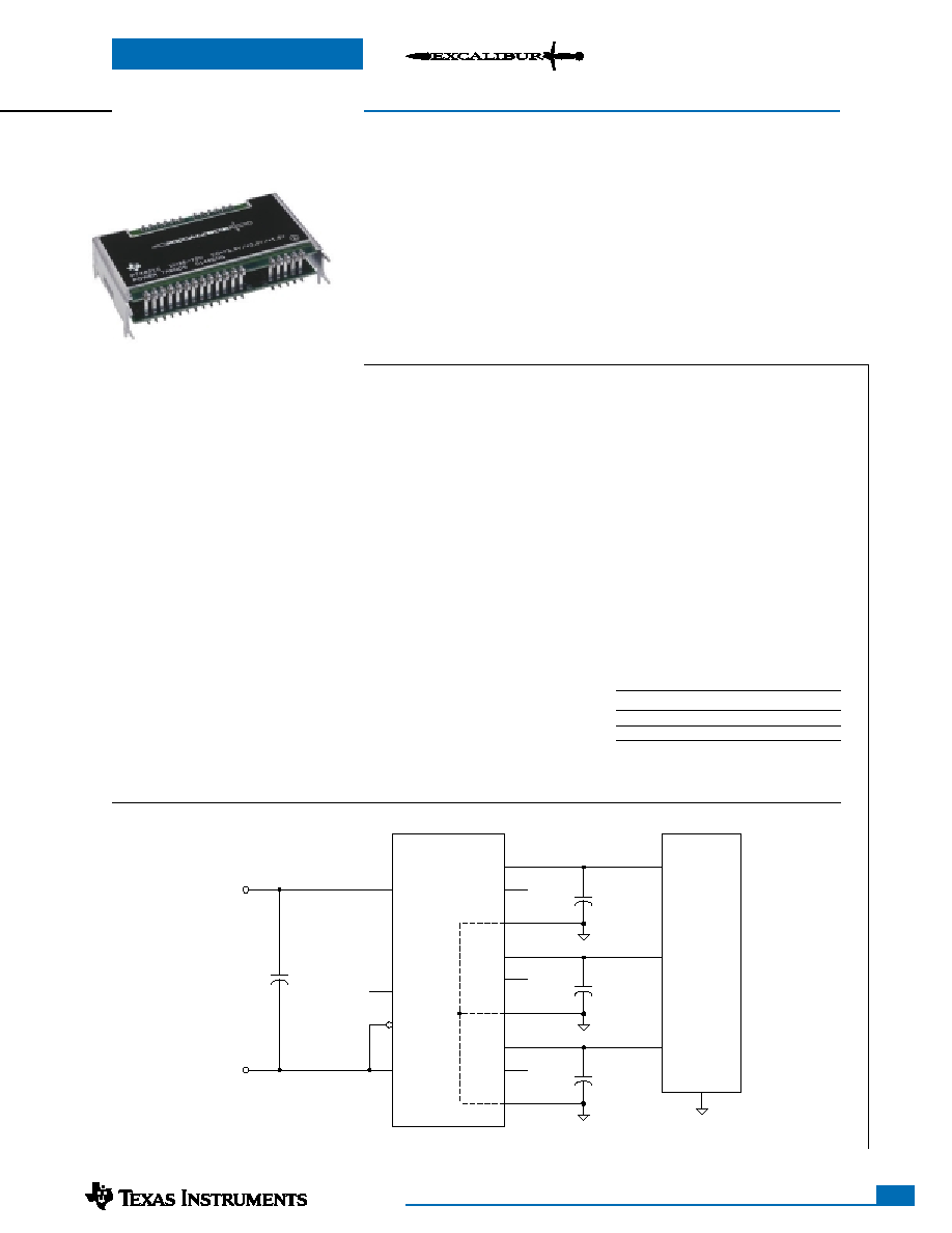
Typical Application
PT4820 Series
Description
The PT4820 ExcaliburTM power
modules are a series of isolated triple-
output DC/DC converters that
operate from a standard (≠48V)
central office supply. Rated for up to
35W, these regulators are ideal for
powering many mixed logic appli-
cations. The triple-output voltage
combination allows for a compact
multiple-output power supply in a
single low-profile DC/DC module.
The available output voltage
options include a low-voltage power
bus for a DSP or ASIC core, and
two additional standard logic supply
voltages.
The PT4820 series incorporates
many features to simplify system
integration. These include a flexible
On/Off enable control, an input
under-voltage lock-out, and over-
temperature protection. All outputs
have short-circuit protection and are
internally sequenced to meet the
power-up and power-down require-
ments of popular DSP ICs.
The PT4820 series is housed in
a space-saving solderable case. The
module requires no external heat sink
and can occupy as little as 1.3 in
2
of
PCB area.
Cin
= Optional
Co
1
, Co
2
, Co
3
= Optional; See specifications
EN1 & EN2 pins:
See On/Off Enable Logic
35-W Triple Output Isolated DC/DC
Converter for Logic Applications
C
IN
+
Co
3
+
Co
2
+
Co
1
+
DSL, DSP,
or ASIC
Chipset
I/O
Logic
Core
+V
IN
≠V
IN
18
PT4820
EN 2
EN 1
+Vo
1
+Vo
2
+Vo
3
COM
V
1
Adj
V
2
Adj
V
3
Adj
COM
+V
IN
≠V
IN
12,13
11
16,17
15
20,21
19
9,10
3
1
2
4
COM 14
∑
Over-Temperature Shutdown
∑
Under-Voltage Lockout
∑
Space Saving Package:
1.3 sq. in. PCB Area (suffix N)
∑
Solderable Copper Case
∑
Safety Approvals:
UL60950
CSA 22.2 950
VDE EN60950

For technical support and more information, see inside back cover or visit www.ti.com
2
SLTS165E - FEBRUARY 2002 - REVISED MARCH 2003
Pin Function
1
EN 1
2
EN 2
3
+Vin
4
≠Vin
5
Do Not Connect
6
Pin Not Present
7
Pin Not Present
8
Pin Not Present
9
COM
10
COM
11
Vo
1
Adjust
PT4820 Series
35-W Triple Output Isolated DC/DC
Converter for Logic Applications
Pin Function
12
Vo
1
13
Vo
1
14
COM
15
Vo
2
adjust
16
+Vo
2
17
+Vo
2
18
COM
19
Vo
3
adjust
20
+Vo
3
21
+Vo
3
On/Off Enable Logic
Pin Configuration
Pin Descriptions
Pin 1
Pin 2
Output Status
◊
1
Off
1
0
On
0
◊
Off
Notes:
Logic 1 =Open collector
Logic 0 = ≠Vin (pin 2) potential
For positive Enable function, connect pin 2
to pin 4 and use pin 1.
For negative Enable function, leave pin 1
open and use pin 2.
For automatice power-up connect pin 2 to
pin 4 and leave pin 1 open.
+Vin:
The positive input supply for the module with
respect to ≠Vin. When powering the module from a
≠48V telecom central office supply, this input is
connected to the primary system ground.
≠Vin:
The negative input supply for the module, and
the 0VDC reference for the EN 1, and EN 2 inputs.
When powering the module from a +48V supply,
this input is connected to the 48V(Return).
EN 1:
The positive logic input that activates the
module output. If not used, this pin should be left
open circuit. Connecting this input to ≠Vin disables
the module's outputs.
EN 2:
The negative logic input that activates the
module output. This pin must be connected to ≠Vin
to enable the module's outputs. A high impedance
disables the module's outputs.
Vo 1:
The highest regulated output voltage, which is
referenced to the COM node.
Vo 2:
The regulated output that is designed to power
logic circuitry. It is referenced to the COM node.
Vo 3:
The low-voltage regulated output that provides
power for a µ-processor or DSP core, and is refer-
enced to the COM node.
COM:
The secondary return reference for the module's
three regulated output voltages. It is DC isolated from
the input supply pins.
Vo
1
Adjust:
Using a single resistor, this pin allows Vo
1
to be adjusted higher or lower than the preset value.
If not used, this pin should be left open circuit.
Vo
2
Adjust:
Using a single resistor, this pin allows Vo
2
to be adjusted higher or lower than the preset value.
If not used, this pin should be left open circuit.
Vo
3
Adjust:
Using a single resistor, this pin allows Vo
3
to be adjusted higher or lower than the preset value.
If not used, this pin should be left open circuit.
Note: Shaded functions indicates those pins that are at primary-side
potential. All other pins are referenced to the secondary.
Environmental Specifications
Characteristics
Symbols
Conditions
Min
Typ
Max
Units
Ambient Temperature Range
T
a
Over V
in
Range
≠40
--
+85
(i)
∞C
Case Temperature
T
c
Measured at center of case
--
--
+100
∞C
ShutdownTemperature
OTP
115
125
∞C
Solder Reflow Temperature
T
reflow
Surface temperature of module pins or case
--
--
215
(ii)
∞C
Storage Temperature
T
s
--
≠40
--
+125
∞C
Mechanical Shock
Per Mil-STD-883D, Method 2002.3
1 msec, Ω Sine, mounted
--
500
--
G's
Mechanical Vibration
Mil-STD-883D, Method 2007.2
Suffix A, C
--
20
(iii)
--
G's
20-2000 Hz
Weight
--
Vertical/Horizontal
--
50
--
grams
Flammability
--
Meets UL 94V-O
Notes:
(i) See SOA curves or consult factory for appropriate derating.
(ii) During solder reflow of SMD package version, do not elevate the module case, pins, or internal component temperatures above a peak of 215∞C. For
further guidance refer to the application note, "Reflow Soldering Requirements for Plug-in Power Surface Mount Products," (SLTA051).
(iii) The case pins on through-hole pin configurations (N & A) must be soldered. For more information see the applicable package outline drawing.
For technical support and more information, see inside back cover or visit www.ti.com
3
SLTS165E - FEBRUARY 2002 - REVISED MARCH 2003
PT4821--48V
35-W Triple Output Isolated DC/DC
Converter for Logic Applications
PT4821 Electrical Specifications
(Unless otherwise stated, the operating conditions are: T
a
=25∞C, V
in
=48V, and I
o
=0.5I
o
max)
PT4821
Characteristics
Symbols
Conditions
Min
Typ
Max
Units
Output Current
I
o
Each output
Io
1
(3.3V)
0.25
(1)
--
8
(2)
Io
2
(2.5V)
0.1
(1)
--
6
(2)
A
Io
3
(1.5V)
0.1
(1)
--
6
(2)
Total (Io
1
+ Io
2
+ Io
3
)
--
--
12
(2)
A
Input Voltage Range
V
in
Continuous
36
--
75
V
Surge (1 minute)
--
--
80
Set-Point Voltage
V
o
Vo
1
3.24
3.3
3.36
Vo
2
2.45
2.5
2.55
V
Vo
3
1.47
1.5
1.53
Temperature Variation
Reg
temp
≠40∞C
T
a
+85∞C, I
o
=I
o
min
Vo
1
--
±0.5
--
%V
o
Vo
2
/Vo
3
--
±0.5
--
Line Regulation
Reg
line
All outputs, Over V
in
range
--
±0.1
±0.5
%V
o
Load Regulation
Reg
load
All outputs, 0
I
o
I
o
max
--
±0.1
±0.5
%V
o
Total Output Voltage Variation
V
o
tol
Includes set-point, line, load,
Vo
1
--
--
±3
(3)
%V
o
≠40∞C
T
a
+85∞C
Vo
2
/Vo
3
--
--
±3
(3)
Efficiency
Io
1
=6A, Io
2
=2A, Io
3
=2A
--
87
--
%
V
o
Ripple/Noise
V
n
Vo
1
--
40
--
(0 to 20MHz bandwidth)
Vo
2
--
35
--
mV
pp
Vo
3
--
25
--
Transient Response
t
tr
0.1A/µs load step, 50% to 75% I
o
max
--
200
--
µSec
V
os
V
o
over/undershoot
--
3
--
%V
o
Output Adjust Range
V
o
adj
Vo
1
/Vo
2
/Vo
3
--
±10
--
%V
o
Over-Current Threshold
I
TRIP
Total, all outputs. Reset with auto-recovery
--
14
--
A
Switching Frequency
s
Over V
in
and I
o
ranges
350
400
450
kHz
Under Voltage Lockout
V
on
V
in
increasing
--
35.5
--
V
V
off
V
in
decreasing
--
34
--
Turn-On Time
t
on
V
in
=48V step
--
140
(4)
--
ms
Enable Control (pins 1 & 2)
Referenced to ≠V
in
(pin 4)
High-Level Input Voltage
V
IH
4
--
15
(5)
V
Low-Level Input Voltage
V
IL
≠0.2
--
0.8
Low-Level Input Current
I
IL
--
1
2
mA
Standby Input Current
I
in
standby
pins 1 & 2 open circuit
--
1
5
mA
Internal Input Capacitance
C
int
--
1.14
--
µF
External Output Capacitance
Co
1
0
220
1,000
(6)
Co
2
0
220
1,000
(6)
µF
Co
3
0
220
1,000
(6)
Primary/Secondary Isolation
V
iso
1500
--
--
V
C
iso
--
2,200
--
pF
R
iso
10
--
--
M
Notes: (1) The converter will operate down to no load with reduced specifications.
(2) The sum-total current from outputs Vo
1
, Vo
2
, and Vo
3
not to exceed 12ADC.
(3) Limits are specified by design.
(4) Measured from the application of the input voltage to the instance that all outputs are in regulation.
(5) The Enable inputs (pins 1 & 2) have internal pull-ups. Leaving pin 1 open-circuit and connecting pin 2 to ≠V
in
allows the the converter to operate when
input power is applied. The maximum open-circuit voltage is 4V.
(6) Ultra-low ESR capacitors, such as organic or polymer aluminum electrolytic types, may cause instability. Consult the factory before using.

For technical support and more information, see inside back cover or visit www.ti.com
4
SLTS165E - FEBRUARY 2002 - REVISED MARCH 2003
PT4821--48V
35-W Triple Output Isolated DC/DC
Converter for Logic Applications
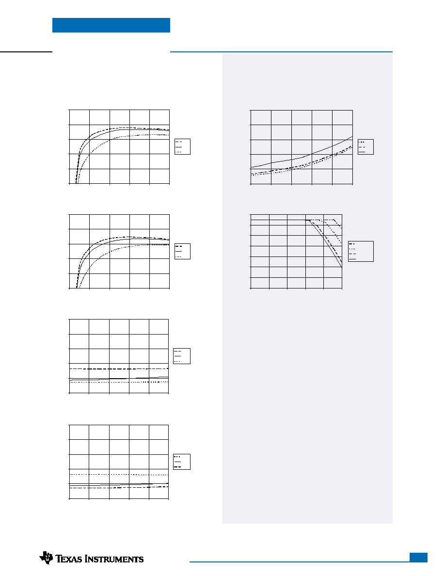
Efficiency vs Output Power
(Io
1
=8A, Io
2
=2A, Io
3
=2A represents 100% Load)
PT4821 Performance Characteristics
(See Notes A, B)
Typical Characteristics
Power Dissipation vs Output Load
Note A:
All Characteristic data in the above graphs has been developed from actual products tested at 25∞C. This data is considered typical data for the ISR.
Note B:
Output Load (%) represents the percent drawn from each output of the stated 100% load condition.
Note C:
SOA curves represent operating conditions at which the internal components are at or below the manufacturer's maximum rated operating temperatures.
Safe Operating Area @V
in
=48V
PT4821 Thermal Performance
(See Note C)
(Io
1
+ Io
2
+ Io
3
=12A, represents 100% Load)
Output Ripple vs Output Power; V
in
=48V
(Io
1
=8A, Io
2
=2A, Io
3
=2A represents 100% Load)
50
60
70
80
90
100
0
20
40
60
80
100
Output Load (%)
Efficiency - %
36V
48V
75V
V
IN
0
20
40
60
80
100
0
20
40
60
80
100
Output Load (%)
Ripple - mV
3.3V
2.5V
1.5V
V
OUT
0
2
4
6
8
0
20
40
60
80
100
Output Load (%)
Pd - Watts
75V
48V
36V
V
IN
50
60
70
80
90
100
0
20
40
60
80
100
Output Load (%)
Efficiency - %
36V
48V
75V
V
IN
0
20
40
60
80
100
0
20
40
60
80
100
Output Load (%)
Ripple - mV
3.3V
2.5V
1.5V
V
OUT
Efficiency vs Output Power
(Io
1
=4A, Io
2
=4A, Io
3
=4A represents 100% Load)
Output Ripple vs Output Power; V
in
=48V
(Io
1
=4A, Io
2
=4A, Io
3
=4A represents 100% Load)
20
30
40
50
60
70
80
90
0%
20%
40%
60%
80%
100%
Output Load (%)
Ambient Temperature (∞C)
200LFM
120LFM
60LFM
Nat conv
Airflow

For technical support and more information, see inside back cover or visit www.ti.com
5
SLTS165E - FEBRUARY 2002 - REVISED MARCH 2003
PT4822--48V
35-W Triple Output Isolated DC/DC
Converter for Logic Applications
PT4822 Electrical Specifications
(Unless otherwise stated, the operating conditions are: T
a
=25∞C, V
in
=48V, and I
o
=0.5I
o
max)
PT4822
Characteristics
Symbols
Conditions
Min
Typ
Max
Units
Output Current
I
o
Each output
Io
1
(3.3V)
0.25
(1)
--
8
(2)
Io
2
(1.8V)
0.1
(1)
--
6
(2)
A
Io
3
(1.5V)
0.1
(1)
--
6
(2)
Total (Io
1
+ Io
2
+ Io
3
)
--
--
12
(2)
A
Input Voltage Range
V
in
Continuous
36
--
75
V
Surge (1 minute)
--
--
80
Set-Point Voltage
V
o
Vo
1
3.24
3.3
3.36
Vo
2
1.76
1.8
1.84
V
Vo
3
1.47
1.5
1.53
Temperature Variation
Reg
temp
≠40∞C
T
a
+85∞C, I
o
=I
o
min
Vo
1
--
±0.5
--
%V
o
Vo
2
/Vo
3
--
±0.5
--
Line Regulation
Reg
line
All outputs, Over V
in
range
--
±0.1
±0.5
%V
o
Load Regulation
Reg
load
All outputs, 0
I
o
I
o
max
--
±0.1
±0.5
%V
o
Total Output Voltage Variation
V
o
tol
Includes set-point, line, load,
Vo
1
--
--
±3
(3)
%V
o
≠40∞C
T
a
+85∞C
Vo
2
/Vo
3
--
--
±3
(3)
Efficiency
Io
1
=6A, Io
2
=2A, Io
3
=2A
--
86
--
%
V
o
Ripple/Noise
V
n
Vo
1
--
40
--
(0 to 20MHz bandwidth)
Vo
2
--
25
--
mV
pp
Vo
3
--
25
--
Transient Response
t
tr
0.1A/µs load step, 50% to 75% I
o
max
--
200
--
µSec
V
os
V
o
over/undershoot
--
3
--
%V
o
Output Adjust Range
V
o
adj
Vo
1
/Vo
2
/Vo
3
--
±10
--
%V
o
Over-Current Threshold
I
TRIP
Total, all outputs. Reset with auto-recovery
--
14
--
A
Switching Frequency
s
Over V
in
and I
o
ranges
350
400
450
kHz
Under Voltage Lockout
V
on
V
in
increasing
--
35.5
--
V
V
off
V
in
decreasing
--
34
--
Turn-On Time
t
on
V
in
=48V step
--
140
(4)
--
ms
Enable Control (pins 1 & 2)
Referenced to ≠V
in
(pin 4)
High-Level Input Voltage
V
IH
4
--
15
(5)
V
Low-Level Input Voltage
V
IL
≠0.2
--
0.8
Low-Level Input Current
I
IL
--
1
2
mA
Standby Input Current
I
in
standby
pins 1 & 2 open circuit
--
1
5
mA
Internal Input Capacitance
C
int
--
1.14
--
µF
External Output Capacitance
Co
1
0
220
1,000
(6)
Co
2
0
220
1,000
(6)
µF
Co
3
0
220
1,000
(6)
Primary/Secondary Isolation
V
iso
1500
--
--
V
C
iso
--
2,200
--
pF
R
iso
10
--
--
M
Notes: (1) The converter will operate down to no load with reduced specifications.
(2) The sum-total current from outputs Vo
1
, Vo
2
, and Vo
3
cannot exceed 12ADC.
(3) Limits are specified by design.
(4) Measured from the application of the input voltage to the instance that all outputs are in regulation.
(5) The Enable inputs (pins 1 & 2) have internal pull-ups. Leaving pin 1 open-circuit and connecting pin 2 to ≠V
in
allows the the converter to operate when
input power is applied. The maximum open-circuit voltage is 4V.
(6) Ultra-low ESR capacitors, such as organic or polymer aluminum electrolytic types, may cause instability. Consult the factory before using.

For technical support and more information, see inside back cover or visit www.ti.com
6
SLTS165E - FEBRUARY 2002 - REVISED MARCH 2003
PT4822--48V
35-W Triple Output Isolated DC/DC
Converter for Logic Applications
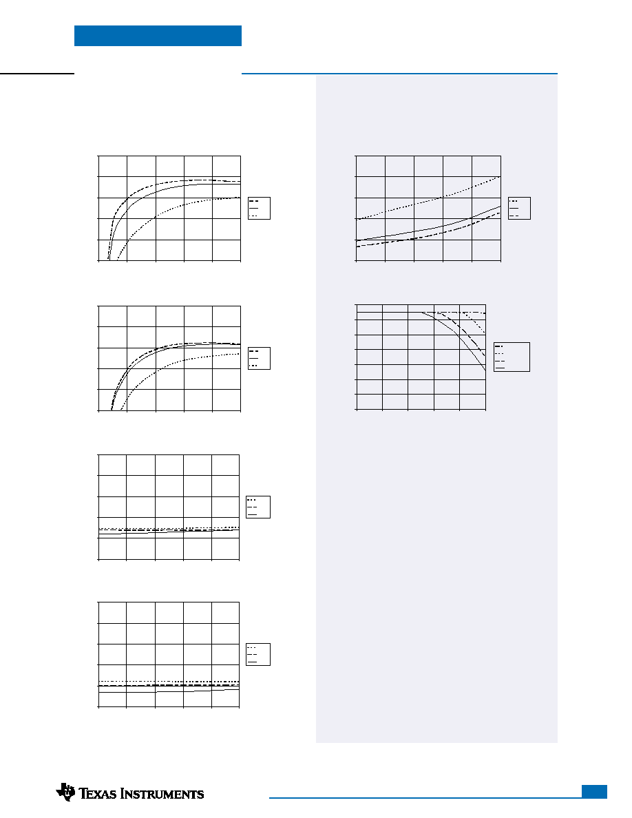
PT4822 Performance Characteristics
(See Note A, B)
Typical Characteristics
Note A:
All Characteristic data in the above graphs has been developed from actual products tested at 25∞C. This data is considered typical data for the ISR.
Note B:
Output Load (%) represents the percent drawn from each output of the stated 100% load condition.
Note C:
SOA curves represent operating conditions at which the internal components are at or below the manufacturer's maximum rated operating temperatures.
PT4822 Thermal Performance
(See Note C)
(Io
1
+ Io
2
+ Io
3
=12A, represents 100% Load)
50
60
70
80
90
100
0
20
40
60
80
100
Output Load (%)
Efficiency - %
36V
48V
75V
V
IN
0
20
40
60
80
100
0
20
40
60
80
100
Output Load (%)
Ripple - mV
3.3V
1.8V
1.5V
V
OUT
0
20
40
60
80
100
0
20
40
60
80
100
Output Load (%)
Ripple - mV
3.3V
1.8V
1.5V
V
OUT
Efficiency vs Output Power
(Io
1
=8A, Io
2
=2A, Io
3
=2A represents 100% Load)
Output Ripple vs Output Power; V
in
=48V
(Io
1
=8A, Io
2
=2A, Io
3
=2A represents 100% Load)
Efficiency vs Output Power
(Io
1
=4A, Io
2
=4A, Io
3
=4A represents 100% Load)
Output Ripple vs Output Power; V
in
=48V
(Io
1
=4A, Io
2
=4A, Io
3
=4A represents 100% Load)
50
60
70
80
90
100
0
20
40
60
80
100
Output Load (%)
Efficiency - %
36V
48V
75V
V
IN
0
2
4
6
8
0
20
40
60
80
100
Output Load (%)
Pd - Watts
75V
48V
36V
V
IN
Power Dissipation vs Output Load
20
30
40
50
60
70
80
90
0%
20%
40%
60%
80%
100%
Output Load (%)
Ambient Temperature (
∞
C)
200LFM
120LFM
60LFM
Nat Conv
Airflow
Safe Operating Area @V
in
=48V

For technical support and more information, see inside back cover or visit www.ti.com
7
SLTS165E - FEBRUARY 2002 - REVISED MARCH 2003
PT4823--48V
35-W Triple Output Isolated DC/DC
Converter for Logic Applications
PT4823 Electrical Specifications
(Unless otherwise stated, the operating conditions are: T
a
=25∞C, V
in
=48V, and I
o
=0.5I
o
max)
PT4823
Characteristics
Symbols
Conditions
Min
Typ
Max
Units
Output Current
I
o
Each output
Io
1
(3.3V)
0.25
(1)
--
8
(2)
Io
2
(2.5V)
0.1
(1)
--
6
(2)
A
Io
3
(1.2V)
0.1
(1)
--
6
(2)
Total (Io
1
+ Io
2
+ Io
3
)
--
--
12
(2)
A
Input Voltage Range
V
in
Continuous
36
--
75
V
Surge (1 minute)
--
--
80
Set-Point Voltage
V
o
Vo
1
3.24
3.3
3.36
Vo
2
2.45
2.5
2.55
V
Vo
3
1.17
1.2
1.23
Temperature Variation
Reg
temp
≠40∞C
T
a
+85∞C, I
o
=I
o
min
Vo
1
--
±0.5
--
%V
o
Vo
2
/Vo
3
--
±0.5
--
Line Regulation
Reg
line
All outputs, Over V
in
range
--
±0.1
±0.5
%V
o
Load Regulation
Reg
load
All outputs, 0
I
o
I
o
max
--
±0.1
±0.5
%V
o
Total Output Voltage Variation
V
o
tol
Includes set-point, line, load,
Vo
1
--
--
±3
(3)
%V
o
≠40∞C
T
a
+85∞C
Vo
2
/Vo
3
--
--
±3
(3)
Efficiency
Io
1
=6A, Io
2
=2A, Io
3
=2A
--
85.6
--
%
V
o
Ripple/Noise
V
n
Vo
1
--
35
--
(0 to 20MHz bandwidth)
Vo
2
--
25
--
mV
pp
Vo
3
--
25
--
Transient Response
t
tr
0.1A/µs load step, 50% to 75% I
o
max
--
200
--
µSec
V
os
V
o
over/undershoot
--
3
--
%V
o
Output Adjust Range
V
o
adj
Vo
1
/Vo
2
/Vo
3
--
±10
--
%V
o
Over-Current Threshold
I
TRIP
Total, all outputs. Reset with auto-recovery
--
14
--
A
Switching Frequency
s
Over V
in
and I
o
ranges
350
400
450
kHz
Under Voltage Lockout
V
on
V
in
increasing
--
35.5
--
V
V
off
V
in
decreasing
--
34
--
Turn-On Time
t
on
V
in
=48V step
--
140
(4)
--
ms
Enable Control (pins 1 & 2)
Referenced to ≠V
in
(pin 4)
High-Level Input Voltage
V
IH
4
--
15
(5)
V
Low-Level Input Voltage
V
IL
≠0.2
--
0.8
Low-Level Input Current
I
IL
--
1
2
mA
Standby Input Current
I
in
standby
pins 1 & 2 open circuit
--
1
5
mA
Internal Input Capacitance
C
int
--
1.14
--
µF
External Output Capacitance
Co
1
0
220
1,000
(6)
Co
2
0
220
1,000
(6)
µF
Co
3
0
220
1,000
(6)
Primary/Secondary Isolation
V
iso
1500
--
--
V
C
iso
--
2,200
--
pF
R
iso
10
--
--
M
Notes: (1) The converter will operate down to no load with reduced specifications.
(2) The sum-total current from outputs Vo
1
, Vo
2
, and Vo
3
cannot exceed 12ADC.
(3) Limits are specified by design.
(4) Measured from the application of the input voltage to the instance that all outputs are in regulation.
(5) The Enable inputs (pins 1 & 2) have internal pull-ups. Leaving pin 1 open-circuit and connecting pin 2 to ≠V
in
allows the the converter to operate when
input power is applied. The maximum open-circuit voltage is 4V.
(6) Ultra-low ESR capacitors, such as organic or polymer aluminum electrolytic types, may cause instability. Consult the factory before using.

For technical support and more information, see inside back cover or visit www.ti.com
8
SLTS165E - FEBRUARY 2002 - REVISED MARCH 2003
PT4823--48V
35-W Triple Output Isolated DC/DC
Converter for Logic Applications
Typical Characteristics
Note A:
All Characteristic data in the above graphs has been developed from actual products tested at 25∞C. This data is considered typical data for the ISR.
Note B:
Output Load (%) represents the percent drawn from each output of the stated 100% load condition.
Note C:
SOA curves represent operating conditions at which the internal components are at or below the manufacturer's maximum rated operating temperatures.
PT4823 Performance Characteristics
(See Notes A, B)
Power Dissipation vs Output Load
PT4823 Thermal Performance
(See Note C)
(Io
1
+ Io
2
+ Io
3
=12A, represents 100% Load)
Efficiency vs Output Power
(Io
1
=8A, Io
2
=2A, Io
3
=2A represents 100% Load)
Output Ripple vs Output Power; V
in
=48V
(Io
1
=8A, Io
2
=2A, Io
3
=2A represents 100% Load)
Efficiency vs Output Power
(Io
1
=4A, Io
2
=4A, Io
3
=4A represents 100% Load)
Output Ripple vs Output Power; V
in
=48V
(Io
1
=4A, Io
2
=4A, Io
3
=4A represents 100% Load)
50
60
70
80
90
100
0
20
40
60
80
100
Output Load (%)
Efficiency - %
36V
48V
75V
V
IN
0
20
40
60
80
100
0
20
40
60
80
100
Output Load (%)
Ripple - mV
2.5V
3.3V
1.2V
V
OUT
0
2
4
6
8
0
20
40
60
80
100
Output Load (%)
Pd - Watts
75V
48V
36V
V
IN
50
60
70
80
90
100
0
20
40
60
80
100
Output Load (%)
Efficiency - %
36V
48V
75V
V
IN
0
20
40
60
80
100
0
20
40
60
80
100
Output Load (%)
Ripple - mV
2.5V
3.3V
1.2V
V
OUT
Safe Operating Area @V
in
=48V
20
30
40
50
60
70
80
90
0%
20%
40%
60%
80%
100%
Output Load (%)
Ambient Temperature (
∞
C)
200LFM
120LFM
60LFM
Nat Conv
Airflow

For technical support and more information, see inside back cover or visit www.ti.com
9
SLTS165E - FEBRUARY 2002 - REVISED MARCH 2003
PT4824--48V
35-W Triple Output Isolated DC/DC
Converter for Logic Applications
PT4824 Electrical Specifications
(Unless otherwise stated, the operating conditions are: T
a
=25∞C, V
in
=48V, and I
o
=0.5I
o
max)
PT4824
Characteristics
Symbols
Conditions
Min
Typ
Max
Units
Output Current
I
o
Each output
Io
1
(3.3V)
0.25
(1)
--
8
(2)
Io
2
(1.8V)
0.1
(1)
--
6
(2)
A
Io
3
(1.2V)
0.1
(1)
--
6
(2)
Total (Io
1
+ Io
2
+ Io
3
)
--
--
12
(2)
A
Input Voltage Range
V
in
Continuous
36
--
75
V
Surge (1 minute)
--
--
80
Set-Point Voltage
V
o
Vo
1
3.24
3.3
3.36
Vo
2
1.76
1.8
1.84
V
Vo
3
1.17
1.2
1.23
Temperature Variation
Reg
temp
≠40∞C
T
a
+85∞C, I
o
=I
o
min
Vo
1
--
±0.5
--
%V
o
Vo
2
/Vo
3
--
±0.5
--
Line Regulation
Reg
line
All outputs, Over V
in
range
--
±0.1
±0.5
%V
o
Load Regulation
Reg
load
All outputs, 0
I
o
I
o
max
--
±0.1
±0.5
%V
o
Total Output Voltage Variation
V
o
tol
Includes set-point, line, load,
Vo
1
--
--
±3
(3)
%V
o
≠40∞C
T
a
+85∞C
Vo
2
/Vo
3
--
--
±3
(3)
Efficiency
Io
1
=6A, Io
2
=2A, Io
3
=2A
--
85
--
%
V
o
Ripple/Noise
V
n
Vo
1
--
30
--
(0 to 20MHz bandwidth)
Vo
2
--
25
--
mV
pp
Vo
3
--
25
--
Transient Response
t
tr
0.1A/µs load step, 50% to 75% I
o
max
--
200
--
µSec
V
os
V
o
over/undershoot
--
3
--
%V
o
Output Adjust Range
V
o
adj
Vo
1
/Vo
2
/Vo
3
--
±10
--
%V
o
Over-Current Threshold
I
TRIP
Total, all outputs. Reset with auto-recovery
--
14
--
A
Switching Frequency
s
Over V
in
and I
o
ranges
350
400
450
kHz
Under Voltage Lockout
V
on
V
in
increasing
--
35.5
--
V
V
off
V
in
decreasing
--
34
--
Turn-On Time
t
on
V
in
=48V step
--
140
(4)
--
ms
Enable Control (pins 1 & 2)
Referenced to ≠V
in
(pin 4)
High-Level Input Voltage
V
IH
4
--
15
(5)
V
Low-Level Input Voltage
V
IL
≠0.2
--
0.8
Low-Level Input Current
I
IL
--
1
2
mA
Standby Input Current
I
in
standby
pins 1 & 2 open circuit
--
1
5
mA
Internal Input Capacitance
C
int
--
1.14
--
µF
External Output Capacitance
Co
1
0
220
1,000
(6)
Co
2
0
220
1,000
(6)
µF
Co
3
0
220
1,000
(6)
Primary/Secondary Isolation
V
iso
1500
--
--
V
C
iso
--
2,200
--
pF
R
iso
10
--
--
M
Notes: (1) The converter will operate down to no load with reduced specifications.
(2) The sum-total current from outputs Vo
1
, Vo
2
, and Vo
3
cannot exceed 12ADC.
(3) Limits are specified by design.
(4) Measured from the application of the input voltage to the instance that all outputs are in regulation.
(5) The Enable inputs (pins 1 & 2) have internal pull-ups. Leaving pin 1 open-circuit and connecting pin 2 to ≠V
in
allows the the converter to operate when
input power is applied. The maximum open-circuit voltage is 4V.
(6) Ultra-low ESR capacitors, such as organic or polymer aluminum electrolytic types, may cause instability. Consult the factory before using.

For technical support and more information, see inside back cover or visit www.ti.com
10
SLTS165E - FEBRUARY 2002 - REVISED MARCH 2003
PT4824--48V
35-W Triple Output Isolated DC/DC
Converter for Logic Applications
Typical Characteristics
Note A:
All Characteristic data in the above graphs has been developed from actual products tested at 25∞C. This data is considered typical data for the ISR.
Note B:
Output Load (%) represents the percent drawn from each output of the stated 100% load condition.
Note C:
SOA curves represent operating conditions at which the internal components are at or below the manufacturer's maximum rated operating temperatures.
PT4824 Performance Characteristics
(See Notes A, B)
Power Dissipation vs Output Load
PT4824 Thermal Performance
(See Note C)
(Io
1
+ Io
2
+ Io
3
=12A, represents 100% Load)
Efficiency vs Output Power
(Io
1
=8A, Io
2
=2A, Io
3
=2A represents 100% Load)
Output Ripple vs Output Power; V
in
=48V
(Io
1
=8A, Io
2
=2A, Io
3
=2A represents 100% Load)
Efficiency vs Output Power
(Io
1
=4A, Io
2
=4A, Io
3
=4A represents 100% Load)
Output Ripple vs Output Power; V
in
=48V
(Io
1
=4A, Io
2
=4A, Io
3
=4A represents 100% Load)
50
60
70
80
90
100
0
20
40
60
80
100
Output Load (%)
Efficiency - %
36V
48V
75V
V
IN
50
60
70
80
90
100
0
20
40
60
80
100
Output Load (%)
Efficiency - %
36V
48V
75V
V
IN
0
20
40
60
80
100
0
20
40
60
80
100
Output Load (%)
Ripple - mV
3.3V
1.8V
1.2V
V
OUT
0
20
40
60
80
100
0
20
40
60
80
100
Output Load (%)
Ripple - mV
3.3V
1.8V
1.2V
V
OUT
0
2
4
6
8
0
20
40
60
80
100
Output Load (%)
Pd - Watts
36V
48V
75V
V
IN
Safe Operating Area @V
in
=48V
20
30
40
50
60
70
80
90
0%
20%
40%
60%
80%
100%
Output Load (%)
Ambient Temperature (
∞
C)
200LFM
120LFM
60LFM
Nat Conv
Airflow

For technical support and more information, see inside back cover or visit www.ti.com
11
SLTS165E - FEBRUARY 2002 - REVISED MARCH 2003
PT4825--48V
35-W Triple Output Isolated DC/DC
Converter for Logic Applications
PT4825 Electrical Specifications
(Unless otherwise stated, the operating conditions are: T
a
=25∞C, V
in
=48V, and I
o
=0.5I
o
max)
PT4825
Characteristics
Symbols
Conditions
Min
Typ
Max
Units
Output Current
I
o
Each output
Io
1
(3.3V)
0.25
(1)
--
8
(2)
Io
2
(1.5V)
0.1
(1)
--
6
(2)
A
Io
3
(1.2V)
0.1
(1)
--
6
(2)
Total (Io
1
+ Io
2
+ Io
3
)
--
--
12
(2)
A
Input Voltage Range
V
in
Continuous
36
--
75
V
Surge (1 minute)
--
--
80
Set-Point Voltage
V
o
Vo
1
3.24
3.3
3.36
Vo
2
1.47
1.5
1.53
V
Vo
3
1.17
1.2
1.23
Temperature Variation
Reg
temp
≠40∞C
T
a
+85∞C, I
o
=I
o
min
Vo
1
--
±0.5
--
%V
o
Vo
2
/Vo
3
--
±0.5
--
Line Regulation
Reg
line
All outputs, Over V
in
range
--
±0.1
±0.5
%V
o
Load Regulation
Reg
load
All outputs, 0
I
o
I
o
max
--
±0.1
±0.5
%V
o
Total Output Voltage Variation
V
o
tol
Includes set-point, line, load,
Vo
1
--
--
±3
(3)
%V
o
≠40∞C
T
a
+85∞C
Vo
2
/Vo
3
--
--
±3
(3)
Efficiency
Io
1
=6A, Io
2
=2A, Io
3
=2A
--
86
--
%
V
o
Ripple/Noise
V
n
Vo
1
--
35
--
(0 to 20MHz bandwidth)
Vo
2
--
25
--
mV
pp
Vo
3
--
25
--
Transient Response
t
tr
0.1A/µs load step, 50% to 75% I
o
max
--
200
--
µSec
V
os
V
o
over/undershoot
--
3
--
%V
o
Output Adjust Range
V
o
adj
Vo
1
/Vo
2
/Vo
3
--
±10
--
%V
o
Over-Current Threshold
I
TRIP
Total, all outputs. Reset with auto-recovery
--
14
--
A
Switching Frequency
s
Over V
in
and I
o
ranges
350
400
450
kHz
Under Voltage Lockout
V
on
V
in
increasing
--
35.5
--
V
V
off
V
in
decreasing
--
34
--
Turn-On Time
t
on
V
in
=48V step
--
140
(4)
--
ms
Enable Control (pins 1 & 2)
Referenced to ≠V
in
(pin 4)
High-Level Input Voltage
V
IH
4
--
15
(5)
V
Low-Level Input Voltage
V
IL
≠0.2
--
0.8
Low-Level Input Current
I
IL
--
1
2
mA
Standby Input Current
I
in
standby
pins 1 & 2 open circuit
--
1
5
mA
Internal Input Capacitance
C
int
--
1.14
--
µF
External Output Capacitance
Co
1
0
220
1,000
(6)
Co
2
0
220
1,000
(6)
µF
Co
3
0
220
1,000
(6)
Primary/Secondary Isolation
V
iso
1500
--
--
V
C
iso
--
2,200
--
pF
R
iso
10
--
--
M
Notes: (1) The converter will operate down to no load with reduced specifications.
(2) The sum-total current from outputs Vo
1
, Vo
2
, and Vo
3
not to exceed 12ADC.
(3) Limits are specified by design.
(4) Measured from the application of the input voltage to the instance that all outputs are in regulation.
(5) The Enable inputs (pins 1 & 2) have internal pull-ups. Leaving pin 1 open-circuit and connecting pin 2 to ≠V
in
allows the the converter to operate when
input power is applied. The maximum open-circuit voltage is 4V.
(6) Ultra-low ESR capacitors, such as organic or polymer aluminum electrolytic types, may cause instability. Consult the factory before using.
For technical support and more information, see inside back cover or visit www.ti.com
12
SLTS165E - FEBRUARY 2002 - REVISED MARCH 2003
PT4825--48V
35-W Triple Output Isolated DC/DC
Converter for Logic Applications
PT4825 Performance Characteristics
(See Notes A, B)
Typical Characteristics
Power Dissipation vs Output Load
Note A:
All Characteristic data in the above graphs has been developed from actual products tested at 25∞C. This data is considered typical data for the ISR.
Note B:
Output Load (%) represents the percent drawn from each output of the stated 100% load condition.
Note C:
SOA curves represent operating conditions at which the internal components are at or below the manufacturer's maximum rated operating temperatures.
PT4825 Thermal Performance
(See Note C)
(Io
1
+ Io
2
+ Io
3
=12A, represents 100% Load)
50
60
70
80
90
100
0
20
40
60
80
100
Output Load (%)
Efficiency - %
36V
48V
75V
V
IN
0
20
40
60
80
100
0
20
40
60
80
100
Output Load (%)
Ripple - mV
3.3V
1.2V
1.5V
V
OUT
0
2
4
6
8
10
0
20
40
60
80
100
Output Load (%)
Pd - Watts
36V
48V
75V
V
IN
50
60
70
80
90
100
0
20
40
60
80
100
Output Load (%)
Efficiency - %
36V
48V
75V
V
IN
0
20
40
60
80
100
0
20
40
60
80
100
Output Load (%)
Ripple - mV
3.3V
1.2V
1.5V
V
OUT
Efficiency vs Output Power
(Io
1
=8A, Io
2
=2A, Io
3
=2A represents 100% Load)
Output Ripple vs Output Power; V
in
=48V
(Io
1
=8A, Io
2
=2A, Io
3
=2A represents 100% Load)
Efficiency vs Output Power
(Io
1
=4A, Io
2
=4A, Io
3
=4A represents 100% Load)
Output Ripple vs Output Power; V
in
=48V
(Io
1
=4A, Io
2
=4A, Io
3
=4A represents 100% Load)
Safe Operating Area @V
in
=48V
20
30
40
50
60
70
80
90
0%
20%
40%
60%
80%
100%
Output Load (%)
Ambient Temperature (
∞
C)
200LFM
120LFM
60LFM
Nat Conv
Airflow

For technical support and more information, see inside back cover or visit www.ti.com
13
SLTS165E - FEBRUARY 2002 - REVISED MARCH 2003
PT4826--48V
35-W Triple Output Isolated DC/DC
Converter for Logic Applications
PT4826 Electrical Specifications
(Unless otherwise stated, the operating conditions are: T
a
=25∞C, V
in
=48V, and I
o
=0.5I
o
max)
PT4826
Characteristics
Symbols
Conditions
Min
Typ
Max
Units
Output Current
I
o
Each output
Io
1
(5.0V)
0.25
(1)
--
5.0
(2)
Io
2
(3.3V)
0.1
(1)
--
5.5
(2)
A
Io
3
(1.8V)
0.1
(1)
--
5.5
(2)
Total (Io
1
+ Io
2
+ Io
3
)
--
--
9
(2)
A
Input Voltage Range
V
in
Continuous
36
--
75
V
Surge (1 minute)
--
--
80
Set-Point Voltage
V
o
Vo
1
4.9
5.0
5.1
Vo
2
3.24
3.3
3.36
V
Vo
3
1.76
1.8
1.84
Temperature Variation
Reg
temp
≠40∞C
T
a
+85∞C, I
o
=I
o
min
Vo
1
--
±0.5
--
%V
o
Vo
2
/Vo
3
--
±0.5
--
Line Regulation
Reg
line
All outputs, Over V
in
range
--
±0.1
±0.5
%V
o
Load Regulation
Reg
load
All outputs, 0
I
o
I
o
max
--
±0.1
±0.5
%V
o
Total Output Voltage Variation
V
o
tol
Includes set-point, line, load,
Vo
1
--
--
±3
(3)
%V
o
≠40∞C
T
a
+85∞C
Vo
2
/Vo
3
--
--
±3
(3)
Efficiency
Io
1
=5A, Io
2
=2A, Io
3
=2A
--
87
--
%
V
o
Ripple/Noise
V
n
Vo
1
--
40
--
(0 to 20MHz bandwidth)
Vo
2
--
35
--
mV
pp
Vo
3
--
25
--
Transient Response
t
tr
0.1A/µs load step, 50% to 75% I
o
max
--
200
--
µSec
V
os
V
o
over/undershoot
--
5
--
%V
o
Output Adjust Range
V
o
adj
Vo
1
/Vo
2
/Vo
3
--
±10
--
%V
o
Over-Current Threshold
I
TRIP
Total, all outputs. Reset with auto-recovery
--
11
--
A
Switching Frequency
s
Over V
in
and I
o
ranges
350
400
450
kHz
Under Voltage Lockout
V
on
V
in
increasing
--
35.5
--
V
V
off
V
in
decreasing
--
34
--
Turn-On Time
t
on
V
in
=48V step
--
140
(4)
--
ms
Enable Control (pins 1 & 2)
Referenced to ≠V
in
(pin 4)
High-Level Input Voltage
V
IH
4
--
15
(5)
V
Low-Level Input Voltage
V
IL
≠0.2
--
0.8
Low-Level Input Current
I
IL
--
1
2
mA
Standby Input Current
I
in
standby
pins 1 & 2 open circuit
--
1
5
mA
Internal Input Capacitance
C
int
--
1.14
--
µF
External Output Capacitance
Co
1
0
220
1,000
(6)
Co
2
0
220
1,000
(6)
µF
Co
3
0
220
1,000
(6)
Primary/Secondary Isolation
V
iso
1500
--
--
V
C
iso
--
2,200
--
pF
R
iso
10
--
--
M
Notes: (1) The converter will operate down to no load with reduced specifications.
(2) The sum-total current from outputs Vo
1
, Vo
2
, and Vo
3
cannot exceed 9ADC.
(3) Limits are specified by design.
(4) Measured from the application of the input voltage to the instance that all outputs are in regulation.
(5) The Enable inputs (pins 1 & 2) have internal pull-ups. Leaving pin 1 open-circuit and connecting pin 2 to ≠V
in
allows the the converter to operate when
input power is applied. The maximum open-circuit voltage is 4V.
(6) Ultra-low ESR capacitors, such as organic or polymer aluminum electrolytic types, may cause instability. Consult the factory before using.

For technical support and more information, see inside back cover or visit www.ti.com
14
SLTS165E - FEBRUARY 2002 - REVISED MARCH 2003
PT4826--48V
35-W Triple Output Isolated DC/DC
Converter for Logic Applications
PT4826 Performance Characteristics
(See Notes A, B)
Typical Characteristics
Power Dissipation vs Output Load
Note A:
All Characteristic data in the above graphs has been developed from actual products tested at 25∞C. This data is considered typical data for the ISR.
Note B:
Output Load (%) represents the percent drawn from each output of the stated 100% load condition.
Note C:
SOA curves represent operating conditions at which the internal components are at or below the manufacturer's maximum rated operating temperatures.
PT4826 Thermal Performance
(See Note C)
(Io
1
+ Io
2
+ Io
3
=9A, represents 100% Load)
50
60
70
80
90
100
0
20
40
60
80
100
Output Load (%)
Efficiency - %
36V
48V
75V
V
IN
0
20
40
60
80
100
0
20
40
60
80
100
Output Load (%)
Ripple - mV
3.3V
1.8V
5.0V
V
OUT
Efficiency vs Output Power
(Io
1
=5A, Io
2
=2A, Io
3
=2A represents 100% Load)
Output Ripple vs Output Power; V
in
=48V
(Io
1
=5A, Io
2
=2A, Io
3
=2A represents 100% Load)
Efficiency vs Output Power
(Io
1
=2A, Io
2
=2A, Io
3
=5A represents 100% Load)
Output Ripple vs Output Power; V
in
=48V
(Io
1
=2A, Io
2
=2A, Io
3
=5A represents 100% Load)
50
60
70
80
90
100
0
20
40
60
80
100
Output Load (%)
Efficiency - %
36V
48V
75V
V
IN
0
20
40
60
80
100
0
20
40
60
80
100
Output Load (%)
Ripple - mV
3.3V
1.8V
5V
V
OUT
0
2
4
6
8
10
0
20
40
60
80
100
Output Load (%)
Pd - Watts
75V
48V
36V
V
IN
Safe Operating Area @V
in
=48V
20
30
40
50
60
70
80
90
0%
20%
40%
60%
80%
100%
Output Load (%)
Ambient Temperature (
∞
C)
200LFM
120LFM
60LFM
Nat Conv
Airflow

For technical support and more information, see inside back cover or visit www.ti.com
15
SLTS165E - FEBRUARY 2002 - REVISED MARCH 2003
PT4827--48V
35-W Triple Output Isolated DC/DC
Converter for Logic Applications
PT4827 Electrical Specifications
(Unless otherwise stated, the operating conditions are: T
a
=25∞C, V
in
=48V, and I
o
=0.5I
o
max)
PT4827
Characteristics
Symbols
Conditions
Min
Typ
Max
Units
Output Current
I
o
Each output
Io
1
(3.3V)
0.25
(1)
--
8
(2)
Io
2
(2.5V)
0.1
(1)
--
6
(2)
A
Io
3
(1.8V)
0.1
(1)
--
6
(2)
Total (Io
1
+ Io
2
+ Io
3
)
--
--
12
(2)
A
Input Voltage Range
V
in
Continuous
36
--
75
V
Surge (1 minute)
--
--
80
Set-Point Voltage
V
o
Vo
1
3.24
3.3
3.36
Vo
2
2.45
2.5
2.55
V
Vo
3
1.76
1.8
1.84
Temperature Variation
Reg
temp
≠40∞C
T
a
+85∞C, I
o
=I
o
min
Vo
1
--
±0.5
--
%V
o
Vo
2
/Vo
3
--
±0.5
--
Line Regulation
Reg
line
All outputs, Over V
in
range
--
±0.1
±0.5
%V
o
Load Regulation
Reg
load
All outputs, 0
I
o
I
o
max
--
±0.1
±0.5
%V
o
Total Output Voltage Variation
V
o
tol
Includes set-point, line, load,
Vo
1
--
--
±3
(3)
%V
o
≠40∞C
T
a
+85∞C
Vo
2
/Vo
3
--
--
±3
(3)
Efficiency
Io
1
=6A, Io
2
=2A, Io
3
=2A
--
86
--
%
V
o
Ripple/Noise
V
n
Vo
1
--
40
--
(0 to 20MHz bandwidth)
Vo
2
--
35
--
mV
pp
Vo
3
--
25
--
Transient Response
t
tr
0.1A/µs load step, 50% to 75% I
o
max
--
200
--
µSec
V
os
V
o
over/undershoot
--
3
--
%V
o
Output Adjust Range
V
o
adj
Vo
1
/Vo
2
/Vo
3
--
±10
--
%V
o
Over-Current Threshold
I
TRIP
Total, all outputs. Reset with auto-recovery
--
14
--
A
Switching Frequency
s
Over V
in
and I
o
ranges
350
400
450
kHz
Under Voltage Lockout
V
on
V
in
increasing
--
35.5
--
V
V
off
V
in
decreasing
--
34
--
Turn-On Time
t
on
V
in
=48V step
--
140
(4)
--
ms
Enable Control (pins 1 & 2)
Referenced to ≠V
in
(pin 4)
High-Level Input Voltage
V
IH
4
--
15
(5)
V
Low-Level Input Voltage
V
IL
≠0.2
--
0.8
Low-Level Input Current
I
IL
--
1
2
mA
Standby Input Current
I
in
standby
pins 1 & 2 open circuit
--
1
5
mA
Internal Input Capacitance
C
int
--
1.14
--
µF
External Output Capacitance
Co
1
0
220
1,000
(6)
Co
2
0
220
1,000
(6)
µF
Co
3
0
220
1,000
(6)
Primary/Secondary Isolation
V
iso
1500
--
--
V
C
iso
--
2,200
--
pF
R
iso
10
--
--
M
Notes: (1) The converter will operate down to no load with reduced specifications.
(2) The sum-total current from outputs Vo
1
, Vo
2
, and Vo
3
cannot exceed 12ADC.
(3) Limits are specified by design.
(4) Measured from the application of the input voltage to the instance that all outputs are in regulation.
(5) The Enable inputs (pins 1 & 2) have internal pull-ups. Leaving pin 1 open-circuit and connecting pin 2 to ≠V
in
allows the the converter to operate when
input power is applied. The maximum open-circuit voltage is 4V.
(6) Ultra-low ESR capacitors, such as organic or polymer aluminum electrolytic types, may cause instability. Consult the factory before using.

For technical support and more information, see inside back cover or visit www.ti.com
16
SLTS165E - FEBRUARY 2002 - REVISED MARCH 2003
PT4827--48V
35-W Triple Output Isolated DC/DC
Converter for Logic Applications
Typical Characteristics
Note A:
All Characteristic data in the above graphs has been developed from actual products tested at 25∞C. This data is considered typical data for the ISR.
Note B:
Output Load (%) represents the percent drawn from each output of the stated 100% load condition.
Note C:
SOA curves represent operating conditions at which the internal components are at or below the manufacturer's maximum rated operating temperatures.
PT4827 Performance Characteristics
(See Notes A, B)
Power Dissipation vs Output Load
PT4827 Thermal Performance
(See Note C)
(Io
1
+ Io
2
+ Io
3
=12A, represents 100% Load)
Efficiency vs Output Power
(Io
1
=8A, Io
2
=2A, Io
3
=2A represents 100% Load)
Output Ripple vs Output Power; V
in
=48V
(Io
1
=8A, Io
2
=2A, Io
3
=2A represents 100% Load)
Efficiency vs Output Power
(Io
1
=4A, Io
2
=4A, Io
3
=4A represents 100% Load)
Output Ripple vs Output Power; V
in
=48V
(Io
1
=4A, Io
2
=4A, Io
3
=4A represents 100% Load)
50
60
70
80
90
100
0
20
40
60
80
100
Output Load (%)
Efficiency - %
36V
48V
75V
V
IN
50
60
70
80
90
100
0
20
40
60
80
100
Output Load (%)
Efficiency - %
36V
48V
75V
V
IN
0
20
40
60
80
100
0
20
40
60
80
100
Output Load (%)
Ripple - mV
3.3V
2.5V
1.8V
V
OUT
0
20
40
60
80
100
0
20
40
60
80
100
Output Load (%)
Ripple - mV
3.3V
2.5V
1.8V
V
OUT
0
1
2
3
4
5
6
7
8
0
20
40
60
80
100
Output Load (%)
Pd - Watts
75V
48V
36V
Safe Operating Area @V
in
=48V
20
30
40
50
60
70
80
90
0%
20%
40%
60%
80%
100%
Output Load (%)
Ambient Temperature (
∞
C)
200LFM
120LFM
60LFM
Nat Conv
Airflow

For technical support and more information, see inside back cover or visit www.ti.com
17
SLTS165E - FEBRUARY 2002 - REVISED MARCH 2003
PT4828--48V
35-W Triple Output Isolated DC/DC
Converter for Logic Applications
PT4828 Electrical Specifications
(Unless otherwise stated, the operating conditions are: T
a
=25∞C, V
in
=48V, and I
o
=0.5I
o
max)
PT4828
Characteristics
Symbols
Conditions
Min
Typ
Max
Units
Output Current
I
o
Each output
Io
1
(5.0V)
0.25
(1)
--
5.0
(2)
Io
2
(2.5V)
0.1
(1)
--
5.5
(2)
A
Io
3
(1.5V)
0.1
(1)
--
5.5
(2)
Total (Io
1
+ Io
2
+ Io
3
)
--
--
9
(2)
A
Input Voltage Range
V
in
Continuous
36
--
75
V
Surge (1 minute)
--
--
80
Set-Point Voltage
V
o
Vo
1
4.9
5.0
5.1
Vo
2
2.45
2.5
2.55
V
Vo
3
1.47
1.5
1.53
Temperature Variation
Reg
temp
≠40∞C
T
a
+85∞C, I
o
=I
o
min
Vo
1
--
±0.5
--
%V
o
Vo
2
/Vo
3
--
±0.5
--
Line Regulation
Reg
line
All outputs, Over V
in
range
--
±0.1
±0.5
%V
o
Load Regulation
Reg
load
All outputs, 0
I
o
I
o
max
--
±0.1
±0.5
%V
o
Total Output Voltage Variation
V
o
tol
Includes set-point, line, load,
Vo
1
--
--
±3
(3)
%V
o
≠40∞C
T
a
+85∞C
Vo
2
/Vo
3
--
--
±3
(3)
Efficiency
Io
1
=5A, Io
2
=2A, Io
3
=2A
--
86.5
--
%
V
o
Ripple/Noise
V
n
Vo
1
--
30
--
(0 to 20MHz bandwidth)
Vo
2
--
30
--
mV
pp
Vo
3
--
25
--
Transient Response
t
tr
0.1A/µs load step, 50% to 75% I
o
max
--
200
--
µSec
V
os
V
o
over/undershoot
--
5
--
%V
o
Output Adjust Range
V
o
adj
Vo
1
/Vo
2
/Vo
3
--
±10
--
%V
o
Over-Current Threshold
I
TRIP
Total, all outputs. Reset with auto-recovery
--
11
--
A
Switching Frequency
s
Over V
in
and I
o
ranges
350
400
450
kHz
Under Voltage Lockout
V
on
V
in
increasing
--
35.5
--
V
V
off
V
in
decreasing
--
34
--
Turn-On Time
t
on
V
in
=48V step
--
140
(4)
--
ms
Enable Control (pins 1 & 2)
Referenced to ≠V
in
(pin 4)
High-Level Input Voltage
V
IH
4
--
15
(5)
V
Low-Level Input Voltage
V
IL
≠0.2
--
0.8
Low-Level Input Current
I
IL
--
1
2
mA
Standby Input Current
I
in
standby
pins 1 & 2 open circuit
--
1
5
mA
Internal Input Capacitance
C
int
--
1.14
--
µF
External Output Capacitance
Co
1
0
220
1,000
(6)
Co
2
0
220
1,000
(6)
µF
Co
3
0
220
1,000
(6)
Primary/Secondary Isolation
V
iso
1500
--
--
V
C
iso
--
2,200
--
pF
R
iso
10
--
--
M
Notes: (1) The converter will operate down to no load with reduced specifications.
(2) The sum-total current from outputs Vo
2
, and Vo
3
cannot exceed 9ADC.
(3) Limits are specified by design.
(4) Measured from the application of the input voltage to the instance that all outputs are in regulation.
(5) The Enable inputs (pins 1 & 2) have internal pull-ups. Leaving pin 1 open-circuit and connecting pin 2 to ≠V
in
allows the the converter to operate when
input power is applied. The maximum open-circuit voltage is 4V.
(6) Ultra-low ESR capacitors, such as organic or polymer aluminum electrolytic types, may cause instability. Consult the factory before using.
For technical support and more information, see inside back cover or visit www.ti.com
18
SLTS165E - FEBRUARY 2002 - REVISED MARCH 2003
PT4828--48V
35-W Triple Output Isolated DC/DC
Converter for Logic Applications
PT4828 Performance Characteristics
(See Notes A, B)
Typical Characteristics
Power Dissipation vs Output Load
Note A:
All Characteristic data in the above graphs has been developed from actual products tested at 25∞C. This data is considered typical data for the ISR.
Note B:
Output Load (%) represents the percent drawn from each output of the stated 100% load condition.
Note C:
SOA curves represent operating conditions at which the internal components are at or below the manufacturer's maximum rated operating temperatures.
PT4828 Thermal Performance
(See Note C)
(Io
1
+ Io
2
+ Io
3
=9A ,represents 100% Load)
50
60
70
80
90
100
0
20
40
60
80
100
Output Load (%)
Efficiency - %
36V
48V
75V
V
IN
0
20
40
60
80
100
0
20
40
60
80
100
Iout (A)
Ripple - mV
5.0V
2.5V
1.5V
V
OUT
0
20
40
60
80
100
0
20
40
60
80
100
Output Load (%)
Ripple - mV
5.0V
2.5V
1.5V
V
OUT
Efficiency vs Output Power
(Io
1
=5A, Io
2
=2A, Io
3
=2A represents 100% Load)
Output Ripple vs Output Power; V
in
=48V
(Io
1
=5A, Io
2
=2A, Io
3
=2A represents 100% Load)
Efficiency vs Output Power
(Io
1
=2A, Io
2
=2A, Io
3
=5A represents 100% Load)
Output Ripple vs Output Power; V
in
=48V
(Io
1
=2A, Io
2
=2A, Io
3
=5A represents 100% Load)
0
2
4
6
8
10
0
20
40
60
80
100
Output Load (%)
Pd - Watts
75V
48V
36V
V
IN
50
60
70
80
90
100
0
20
40
60
80
100
Output Load (%)
Efficiency - %
36V
48V
75V
V
IN
Safe Operating Area @V
in
=48V
20
30
40
50
60
70
80
90
0%
20%
40%
60%
80%
100%
Output Load (%)
Ambient Temperature (
∞
C)
200LFM
120LFM
60LFM
Nat Conv
Airflow

For technical support and more information, see inside back cover or visit www.ti.com
19
SLTS165E - FEBRUARY 2002 - REVISED MARCH 2003
PT4829--48V
35-W Triple Output Isolated DC/DC
Converter for Logic Applications
PT4829 Electrical Specifications
(Unless otherwise stated, the operating conditions are: T
a
=25∞C, V
in
=48V, and I
o
=0.5I
o
max)
PT4829
Characteristics
Symbols
Conditions
Min
Typ
Max
Units
Output Current
I
o
Each output
Io
1
(5.0V)
0.25
(1)
--
5.0
(2)
Io
2
(1.8V)
0.1
(1)
--
5.5
(2)
A
Io
3
(1.5V)
0.1
(1)
--
5.5
(2)
Total (Io
1
+ Io
2
+ Io
3
)
--
--
9
(2)
A
Input Voltage Range
V
in
Continuous
36
--
75
V
Surge (1 minute)
--
--
80
Set-Point Voltage
V
o
Vo
1
4.9
5.0
5.1
Vo
2
1.76
1.8
1.84
V
Vo
3
1.47
1.5
1.53
Temperature Variation
Reg
temp
≠40∞C
T
a
+85∞C, I
o
=I
o
min
Vo
1
--
±0.5
--
%V
o
Vo
2
/Vo
3
--
±0.5
--
Line Regulation
Reg
line
All outputs, Over V
in
range
--
±0.1
±0.5
%V
o
Load Regulation
Reg
load
All outputs, 0
I
o
I
o
max
--
±0.1
±0.5
%V
o
Total Output Voltage Variation
V
o
tol
Includes set-point, line, load,
Vo
1
--
--
±3
(3)
%V
o
≠40∞C
T
a
+85∞C
Vo
2
/Vo
3
--
--
±3
(3)
Efficiency
Io
1
=5A, Io
2
=2A, Io
3
=2A
--
86.2
--
%
V
o
Ripple/Noise
V
n
Vo
1
--
35
--
(0 to 20MHz bandwidth)
Vo
2
--
25
--
mV
pp
Vo
3
--
25
--
Transient Response
t
tr
0.1A/µs load step, 50% to 75% I
o
max
--
200
--
µSec
V
os
V
o
over/undershoot
--
5
--
%V
o
Output Adjust Range
V
o
adj
Vo
1
/Vo
2
/Vo
3
--
±10
--
%V
o
Over-Current Threshold
I
TRIP
Total, all outputs. Reset with auto-recovery
--
11
--
A
Switching Frequency
s
Over V
in
and I
o
ranges
350
400
450
kHz
Under Voltage Lockout
V
on
V
in
increasing
--
35.5
--
V
V
off
V
in
decreasing
--
34
--
Turn-On Time
t
on
V
in
=48V step
--
140
(4)
--
ms
Enable Control (pins 1 & 2)
Referenced to ≠V
in
(pin 4)
High-Level Input Voltage
V
IH
4
--
15
(5)
V
Low-Level Input Voltage
V
IL
≠0.2
--
0.8
Low-Level Input Current
I
IL
--
1
2
mA
Standby Input Current
I
in
standby
pins 1 & 2 open circuit
--
1
5
mA
Internal Input Capacitance
C
int
--
1.14
--
µF
External Output Capacitance
Co
1
0
220
1,000
(6)
Co
2
0
220
1,000
(6)
µF
Co
3
0
220
1,000
(6)
Primary/Secondary Isolation
V
iso
1500
--
--
V
C
iso
--
2,200
--
pF
R
iso
10
--
--
M
Notes: (1) The converter will operate down to no load with reduced specifications.
(2) The sum-total current from outputs Vo
2
, and Vo
3
cannot exceed 9ADC.
(3) Limits are specified by design.
(4) Measured from the application of the input voltage to the instance that all outputs are in regulation.
(5) The Enable inputs (pins 1 & 2) have internal pull-ups. Leaving pin 1 open-circuit and connecting pin 2 to ≠V
in
allows the the converter to operate when
input power is applied. The maximum open-circuit voltage is 4V.
(6) Ultra-low ESR capacitors, such as organic or polymer aluminum electrolytic types, may cause instability. Consult the factory before using.
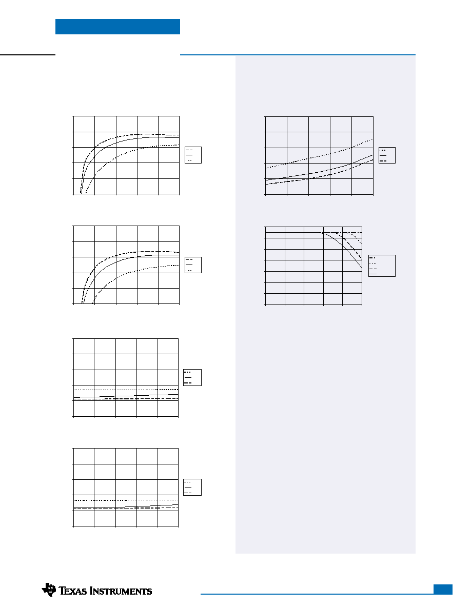
For technical support and more information, see inside back cover or visit www.ti.com
20
SLTS165E - FEBRUARY 2002 - REVISED MARCH 2003
PT4829--48V
35-W Triple Output Isolated DC/DC
Converter for Logic Applications
PT4829 Performance Characteristics
(See Notes A, B)
Typical Characteristics
Power Dissipation vs Output Power
Note A:
All Characteristic data in the above graphs has been developed from actual products tested at 25∞C. This data is considered typical data for the ISR.
Note B:
Output Load (%) represents the percent drawn from each output of the stated 100% load condition.
Note C:
SOA curves represent operating conditions at which the internal components are at or below the manufacturer's maximum rated operating temperatures.
PT4829 Thermal Performance
(See Note C)
(Io
1
+ Io
2
+ Io
3
=9A, represents 100% Load)
50
60
70
80
90
100
0
20
40
60
80
100
Output Load (%)
Efficiency - %
36V
48V
75V
V
IN
0
2
4
6
8
10
0
20
40
60
80
100
Output Load (%)
Pd - Watts
75V
48V
36V
V
IN
50
60
70
80
90
100
0
20
40
60
80
100
Output Load (%)
Efficiency - %
36V
48V
75V
V
IN
0
20
40
60
80
100
0
20
40
60
80
100
Output Load (%)
Ripple - mV
5.0V
1.5V
1.8V
V
OUT
0
20
40
60
80
100
0
20
40
60
80
100
Output Load (%)
Ripple - mV
5.0V
1.5V
1.8V
V
OUT
Efficiency vs Output Power
(Io
1
=5A, Io
2
=2A, Io
3
=2A represents 100% Load)
Output Ripple vs Output Power; V
in
=48V
(Io
1
=5A, Io
2
=2A, Io
3
=2A represents 100% Load)
Efficiency vs Output Power
(Io
1
=2A, Io
2
=2A, Io
3
=5A represents 100% Load)
Output Ripple vs Output Power; V
in
=48V
(Io
1
=2A, Io
2
=2A, Io
3
=5A represents 100% Load)
Safe Operating Area @V
in
=48V
20
30
40
50
60
70
80
90
0%
20%
40%
60%
80%
100%
Output Load (%)
Ambient Temperature (
∞
C)
200LFM
120LFM
60LFM
Nat Conv
Airflow

For technical support and more information, see inside back cover or visit www.ti.com
21
SLTS165E - FEBRUARY 2002 - REVISED MARCH 2003
PT4831--48V
35-W Triple Output Isolated DC/DC
Converter for Logic Applications
PT4831 Electrical Specifications
(Unless otherwise stated, the operating conditions are: T
a
=25∞C, V
in
=48V, and I
o
=0.5I
o
max)
PT4831
Characteristics
Symbols
Conditions
Min
Typ
Max
Units
Output Current
I
o
Each output
Io
1
(5.0V)
0.25
(1)
--
5.0
(2)
Io
2
(3.3V)
0.1
(1)
--
5.5
(2)
A
Io
3
(1.5V)
0.1
(1)
--
5.5
(2)
Total (Io
1
+ Io
2
+ Io
3
)
--
--
9
(2)
A
Input Voltage Range
V
in
Continuous
36
--
75
V
Surge (1 minute)
--
--
80
Set-Point Voltage
V
o
Vo
1
4.9
5.0
5.1
Vo
2
3.24
3.3
3.36
V
Vo
3
1.47
1.5
1.53
Temperature Variation
Reg
temp
≠40∞C
T
a
+85∞C, I
o
=I
o
min
Vo
1
--
±0.5
--
%V
o
Vo
2
/Vo
3
--
±0.5
--
Line Regulation
Reg
line
All outputs, Over V
in
range
--
±0.1
±0.5
%V
o
Load Regulation
Reg
load
All outputs, 0
I
o
I
o
max
--
±0.1
±0.5
%V
o
Total Output Voltage Variation
V
o
tol
Includes set-point, line, load,
Vo
1
--
--
±3
(3)
%V
o
≠40∞C
T
a
+85∞C
Vo
2
/Vo
3
--
--
±3
(3)
Efficiency
Io
1
=5A, Io
2
=2A, Io
3
=2A
--
87
--
%
V
o
Ripple/Noise
V
n
Vo
1
--
40
--
(0 to 20MHz bandwidth)
Vo
2
--
35
--
mV
pp
Vo
3
--
25
--
Transient Response
t
tr
0.1A/µs load step, 50% to 75% I
o
max
--
200
--
µSec
V
os
V
o
over/undershoot
--
5
--
%V
o
Output Adjust Range
V
o
adj
Vo
1
/Vo
2
/Vo
3
--
±10
--
%V
o
Over-Current Threshold
I
TRIP
Total, all outputs. Reset with auto-recovery
--
11
--
A
Switching Frequency
s
Over V
in
and I
o
ranges
350
400
450
kHz
Under Voltage Lockout
V
on
V
in
increasing
--
35.5
--
V
V
off
V
in
decreasing
--
34
--
Turn-On Time
t
on
V
in
=48V step
--
140
(4)
--
ms
Enable Control (pins 1 & 2)
Referenced to ≠V
in
(pin 4)
High-Level Input Voltage
V
IH
4
--
15
(5)
V
Low-Level Input Voltage
V
IL
≠0.2
--
0.8
Low-Level Input Current
I
IL
--
1
2
mA
Standby Input Current
I
in
standby
pins 1 & 2 open circuit
--
1
5
mA
Internal Input Capacitance
C
int
--
1.14
--
µF
External Output Capacitance
Co
1
0
220
1,000
(6)
Co
2
0
220
1,000
(6)
µF
Co
3
0
220
1,000
(6)
Primary/Secondary Isolation
V
iso
1500
--
--
V
C
iso
--
2,200
--
pF
R
iso
10
--
--
M
Notes: (1) The converter will operate down to no load with reduced specifications.
(2) The sum-total current from outputs Vo
1
, Vo
2
, and Vo
3
cannot exceed 9ADC.
(3) Limits are specified by design.
(4) Measured from the application of the input voltage to the instance that all outputs are in regulation.
(5) The Enable inputs (pins 1 & 2) have internal pull-ups. Leaving pin 1 open-circuit and connecting pin 2 to ≠V
in
allows the the converter to operate when
input power is applied. The maximum open-circuit voltage is 4V.
(6) Ultra-low ESR capacitors, such as organic or polymer aluminum electrolytic types, may cause instability. Consult the factory before using.

For technical support and more information, see inside back cover or visit www.ti.com
22
SLTS165E - FEBRUARY 2002 - REVISED MARCH 2003
PT4831--48V
35-W Triple Output Isolated DC/DC
Converter for Logic Applications
Typical Characteristics
Note A:
All Characteristic data in the above graphs has been developed from actual products tested at 25∞C. This data is considered typical data for the ISR.
Note B:
Output Load (%) represents the percent drawn from each output of the stated 100% load condition.
Note C:
SOA curves represent operating conditions at which the internal components are at or below the manufacturer's maximum rated operating temperatures.
50
60
70
80
90
100
0
20
40
60
80
100
Output Load (%)
Efficiency - %
36V
48V
75V
V
IN
0
2
4
6
8
10
0
20
40
60
80
100
Output Power (%)
Pd - Watts
75V
48V
36V
V
IN
50
60
70
80
90
100
0
20
40
60
80
100
Output Load (%)
Efficiency - %
36V
48V
75V
V
IN
PT4831 Performance Characteristics
(See Notes A, B)
Power Dissipation vs Output Power
PT4831 Thermal Performance
(See Note C)
(Io
1
+ Io
2
+ Io
3
=9A, represents 100% Load)
Efficiency vs Output Power
(Io
1
=5A, Io
2
=2A, Io
3
=2A represents 100% Load)
Output Ripple vs Output Power; V
in
=48V
(Io
1
=5A, Io
2
=2A, Io
3
=2A represents 100% Load)
Efficiency vs Output Power
(Io
1
=2A, Io
2
=2A, Io
3
=5A represents 100% Load)
Output Ripple vs Output Power; V
in
=48V
(Io
1
=2A, Io
2
=2A, Io
3
=5A represents 100% Load)
0
20
40
60
80
100
0
20
40
60
80
100
Output Load (%)
Ripple - mV
3.3V
5.0V
1.5V
V
OUT
0
20
40
60
80
100
0
20
40
60
80
100
Output Load (%)
Ripple - mV
3.3V
5.0V
1.5V
V
OUT
Safe Operating Area @V
in
=48V
20
30
40
50
60
70
80
90
0%
20%
40%
60%
80%
100%
Output Load (%)
Ambient Temperature (
∞
C)
200LFM
120LFM
60LFM
Nat Conv
Airflow

For technical support and more information, see inside back cover or visit www.ti.com
23
SLTS165E - FEBRUARY 2002 - REVISED MARCH 2003
PT4832--48V
35-W Triple Output Isolated DC/DC
Converter for Logic Applications
PT4832 Electrical Specifications
(Unless otherwise stated, the operating conditions are: T
a
=25∞C, V
in
=48V, and I
o
=0.5I
o
max)
PT4832
Characteristics
Symbols
Conditions
Min
Typ
Max
Units
Output Current
I
o
Each output
Io
1
(5.0V)
0.25
(1)
--
5.0
(2)
Io
2
(3.3V)
0.1
(1)
--
5.5
(2)
A
Io
3
(2.5V)
0.1
(1)
--
5.5
(2)
Total (Io
1
+ Io
2
+ Io
3
)
--
--
9
(2)
A
Input Voltage Range
V
in
Continuous
36
--
75
V
Surge (1 minute)
--
--
80
Set-Point Voltage
V
o
Vo
1
4.9
5.0
5.1
Vo
2
3.24
3.3
3.36
V
Vo
3
2.45
2.5
2.55
Temperature Variation
Reg
temp
≠40∞C
T
a
+85∞C, I
o
=I
o
min
Vo
1
--
±0.5
--
%V
o
Vo
2
/Vo
3
--
±0.5
--
Line Regulation
Reg
line
All outputs, Over V
in
range
--
±0.1
±0.5
%V
o
Load Regulation
Reg
load
All outputs, 0
I
o
I
o
max
--
±0.1
±0.5
%V
o
Total Output Voltage Variation
V
o
tol
Includes set-point, line, load,
Vo
1
--
--
±3
(3)
%V
o
≠40∞C
T
a
+85∞C
Vo
2
/Vo
3
--
--
±3
(3)
Efficiency
Io
1
=5A, Io
2
=2A, Io
3
=2A
--
86.7
--
%
V
o
Ripple/Noise
V
n
Vo
1
--
30
--
(0 to 20MHz bandwidth)
Vo
2
--
25
--
mV
pp
Vo
3
--
25
--
Transient Response
t
tr
0.1A/µs load step, 50% to 75% I
o
max
--
200
--
µSec
V
os
V
o
over/undershoot
--
5
--
%V
o
Output Adjust Range
V
o
adj
Vo
1
/Vo
2
/Vo
3
--
±10
--
%V
o
Over-Current Threshold
I
TRIP
Total, all outputs. Reset with auto-recovery
--
11
--
A
Switching Frequency
s
Over V
in
and I
o
ranges
350
400
450
kHz
Under Voltage Lockout
V
on
V
in
increasing
--
35.5
--
V
V
off
V
in
decreasing
--
34
--
Turn-On Time
t
on
V
in
=48V step
--
140
(4)
--
ms
Enable Control (pins 1 & 2)
Referenced to ≠V
in
(pin 4)
High-Level Input Voltage
V
IH
4
--
15
(5)
V
Low-Level Input Voltage
V
IL
≠0.2
--
0.8
Low-Level Input Current
I
IL
--
1
2
mA
Standby Input Current
I
in
standby
pins 1 & 2 open circuit
--
1
5
mA
Internal Input Capacitance
C
int
--
1.14
--
µF
External Output Capacitance
Co
1
0
220
1,000
(6)
Co
2
0
220
1,000
(6)
µF
Co
3
0
220
1,000
(6)
Primary/Secondary Isolation
V
iso
1500
--
--
V
C
iso
--
2,200
--
pF
R
iso
10
--
--
M
Notes: (1) The converter will operate down to no load with reduced specifications.
(2) The sum-total current from outputs Vo
2
, and Vo
3
cannot exceed 9ADC.
(3) Limits are specified by design.
(4) Measured from the application of the input voltage to the instance that all outputs are in regulation.
(5) The Enable inputs (pins 1 & 2) have internal pull-ups. Leaving pin 1 open-circuit and connecting pin 2 to ≠V
in
allows the the converter to operate when
input power is applied. The maximum open-circuit voltage is 4V.
(6) Ultra-low ESR capacitors, such as organic or polymer aluminum electrolytic types, may cause instability. Consult the factory before using.

For technical support and more information, see inside back cover or visit www.ti.com
24
SLTS165E - FEBRUARY 2002 - REVISED MARCH 2003
PT4832--48V
35-W Triple Output Isolated DC/DC
Converter for Logic Applications
PT4832 Performance Characteristics
(See Notes A, B)
Typical Characteristics
Power Dissipation vs Output Power
Note A:
All Characteristic data in the above graphs has been developed from actual products tested at 25∞C. This data is considered typical data for the ISR.
Note B:
Output Load (%) represents the percent drawn from each output of the stated 100% load condition.
Note C:
SOA curves represent operating conditions at which the internal components are at or below the manufacturer's maximum rated operating temperatures.
PT4832 Thermal Performance
(See Note C)
(Io
1
+ Io
2
+ Io
3
=9A, represents 100% Load)
Efficiency vs Output Power
(Io
1
=5A, Io
2
=2A, Io
3
=2A represents 100% Load)
Output Ripple vs Output Power; V
in
=48V
(Io
1
=5A, Io
2
=2A, Io
3
=2A represents 100% Load)
Efficiency vs Output Power
(Io
1
=2A, Io
2
=2A, Io
3
=5A represents 100% Load)
Output Ripple vs Output Power; V
in
=48V
(Io
1
=2A, Io
2
=2A, Io
3
=5A represents 100% Load)
50
60
70
80
90
100
0
20
40
60
80
100
Output Load (%)
Efficiency - %
36V
48V
75V
V
IN
50
60
70
80
90
100
0
20
40
60
80
100
Output Load (%)
Efficiency - %
36V
48V
75V
V
IN
0
20
40
60
80
100
0
20
40
60
80
100
Output Load (%)
Ripple - mV
5.0V
3.3V
2.5V
V
OUT
0
20
40
60
80
100
0
20
40
60
80
100
Output Load (%)
Ripple - mV
5.0V
3.3V
2.5V
V
OUT
0
2
4
6
8
0
20
40
60
80
100
Output Load (%)
Pd - Watts
36V
48V
75V
V
IN
Safe Operating Area @V
in
=48V
20
30
40
50
60
70
80
90
0%
20%
40%
60%
80%
100%
Output Load (%)
Ambient Temperature (
∞
C)
200LFM
120LFM
60LFM
Nat Conv
Airflow

For technical support and more information, see inside back cover or visit www.ti.com
25
SLTS165E - FEBRUARY 2002 - REVISED MARCH 2003
PT4833--48V
35-W Triple Output Isolated DC/DC
Converter for Logic Applications
PT4833 Electrical Specifications
(Unless otherwise stated, the operating conditions are: T
a
=25∞C, V
in
=48V, and I
o
=0.5I
o
max)
PT4833
Characteristics
Symbols
Conditions
Min
Typ
Max
Units
Output Current
I
o
Each output
Io
1
(3.3V)
0.25
(1)
--
8
(2)
Io
2
(2.0V)
0.1
(1)
--
6
(2)
A
Io
3
(1.5V)
0.1
(1)
--
6
(2)
Total (Io
1
+ Io
2
+ Io
3
)
--
--
12
(2)
A
Input Voltage Range
V
in
Continuous
36
--
75
V
Surge (1 minute)
--
--
80
Set-Point Voltage
V
o
Vo
1
3.24
3.3
3.36
Vo
2
1.96
2.0
2.04
V
Vo
3
1.47
1.5
1.53
Temperature Variation
Reg
temp
≠40∞C
T
a
+85∞C, I
o
=I
o
min
Vo
1
--
±0.5
--
%V
o
Vo
2
/Vo
3
--
±0.5
--
Line Regulation
Reg
line
All outputs, Over V
in
range
--
±0.1
±0.5
%V
o
Load Regulation
Reg
load
All outputs, 0
I
o
I
o
max
--
±0.1
±0.5
%V
o
Total Output Voltage Variation
V
o
tol
Includes set-point, line, load,
Vo
1
--
--
±3
(3)
%V
o
≠40∞C
T
a
+85∞C
Vo
2
/Vo
3
--
--
±3
(3)
Efficiency
Io
1
=6A, Io
2
=2A, Io
3
=2A
--
86
--
%
V
o
Ripple/Noise
V
n
Vo
1
--
40
--
(0 to 20MHz bandwidth)
Vo
2
--
25
--
mV
pp
Vo
3
--
25
--
Transient Response
t
tr
0.1A/µs load step, 50% to 75% I
o
max
--
200
--
µSec
V
os
V
o
over/undershoot
--
3
--
%V
o
Output Adjust Range
V
o
adj
Vo
1
/Vo
2
/Vo
3
--
±10
--
%V
o
Over-Current Threshold
I
TRIP
Total, all outputs. Reset with auto-recovery
--
14
--
A
Switching Frequency
s
Over V
in
and I
o
ranges
350
400
450
kHz
Under Voltage Lockout
V
on
V
in
increasing
--
35.5
--
V
V
off
V
in
decreasing
--
34
--
Turn-On Time
t
on
V
in
=48V step
--
140
(4)
--
ms
Enable Control (pins 1 & 2)
Referenced to ≠V
in
(pin 4)
High-Level Input Voltage
V
IH
4
--
15
(5)
V
Low-Level Input Voltage
V
IL
≠0.2
--
0.8
Low-Level Input Current
I
IL
--
1
2
mA
Standby Input Current
I
in
standby
pins 1 & 2 open circuit
--
1
5
mA
Internal Input Capacitance
C
int
--
1.14
--
µF
External Output Capacitance
Co
1
0
220
1,000
(6)
Co
2
0
220
1,000
(6)
µF
Co
3
0
220
1,000
(6)
Primary/Secondary Isolation
V
iso
1500
--
--
V
C
iso
--
2,200
--
pF
R
iso
10
--
--
M
Notes: (1) The converter will operate down to no load with reduced specifications.
(2) The sum-total current from outputs Vo
1
, Vo
2
, and Vo
3
cannot exceed 12ADC.
(3) Limits are specified by design.
(4) Measured from the application of the input voltage to the instance that all outputs are in regulation.
(5) The Enable inputs (pins 1 & 2) have internal pull-ups. Leaving pin 1 open-circuit and connecting pin 2 to ≠V
in
allows the the converter to operate when
input power is applied. The maximum open-circuit voltage is 4V.
(6) Ultra-low ESR capacitors, such as organic or polymer aluminum electrolytic types, may cause instability. Consult the factory before using.
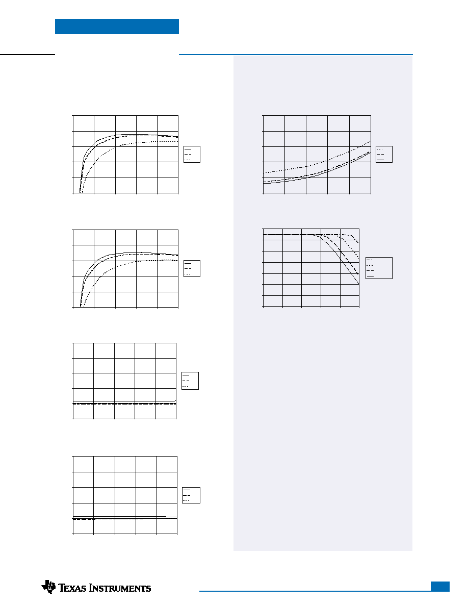
For technical support and more information, see inside back cover or visit www.ti.com
26
SLTS165E - FEBRUARY 2002 - REVISED MARCH 2003
PT4833--48V
35-W Triple Output Isolated DC/DC
Converter for Logic Applications
Typical Characteristics
Note A:
All Characteristic data in the above graphs has been developed from actual products tested at 25∞C. This data is considered typical data for the ISR.
Note B:
Output Load (%) represents the percent drawn from each output of the stated 100% load condition.
Note C:
SOA curves represent operating conditions at which the internal components are at or below the manufacturer's maximum rated operating temperatures.
PT4833 Performance Characteristics
(See Note A, B)
PT4833 Thermal Performance
(See Note C)
(Io
1
+ Io
2
+ Io
3
=12A, represents 100% Load)
Efficiency vs Output Power
(Io
1
=8A, Io
2
=2A, Io
3
=2A represents 100% Load)
Output Ripple vs Output Power; V
in
=48V
(Io
1
=8A, Io
2
=2A, Io
3
=2A represents 100% Load)
Efficiency vs Output Power
(Io
1
=4A, Io
2
=4A, Io
3
=4A represents 100% Load)
Output Ripple vs Output Power; V
in
=48V
(Io
1
=4A, Io
2
=4A, Io
3
=4A represents 100% Load)
Power Dissipation vs Output Load
Safe Operating Area @V
in
=48V
20
30
40
50
60
70
80
90
0%
20%
40%
60%
80%
100%
Output Power (%)
Ambient Temperature (
∞
C)
200LFM
120LFM
60LFM
Nat Conv
Airflow
50
60
70
80
90
100
0
20
40
60
80
100
Output Load (%)
Efficiency - %
36V
48V
75V
V
IN
50
60
70
80
90
100
0
20
40
60
80
100
Output Load (%)
Efficiency - %
36V
48V
75V
V
IN
0
20
40
60
80
100
0
20
40
60
80
100
Output Load (%)
Ripple - mV
3.3V
2.0V
1.5V
V
OUT
0
2
4
6
8
10
0
20
40
60
80
100
Output Load (%)
Pd - Watts
75V
48V
36V
V
IN
0
20
40
60
80
100
0
20
40
60
80
100
Output Load (%)
Ripple - mV
3.3V
2.0V
1.5V
V
OUT

For technical support and more information, see inside back cover or visit www.ti.com
Application Notes
27
PT4820 Series
Operating Features of the PT4820 Triple-Output
DC/DC Converters
Short-Circuit Protection
To protect against load faults the PT4820 series of triple-
output DC/DC converters incorporate output short-circuit
protection. When the combined output current from all
three outputs exceeds the over-current threshold (see data
sheet specifications), the PT4820 shuts down after a short
period of typically 15ms. This forces the output voltage
at all three regulated outputs to simultaneously fall to zero.
Following shutdown, the module automatically attempts
to recover by executing a soft-start power-up. This occurs
at intervals of approximately 65ms. If the load fault persists,
the module will continually cycle through successive over-
current trips and restarts.
Over-Temperature Protection
The PT4820 DC/DC converter series have an internal
temperature sensor, which monitors the temperature of
the module's metal case. If the case temperature exceeds
a nominal 110∞C the converter will shut down. The
converter will automatically restart when the sensed
temperature returns to about 100∞C.
Under-Voltage Lock-Out
The Under-Voltage Lock-Out (UVLO) circuit prevents
operation of the converter whenever the input voltage to
the module is insufficient to maintain output regulation.
The UVLO has approximately 2V of hysterisis. This is
to prevent oscillation with a slowly changing input voltage.
Below the UVLO threshold the module is off and the
enable control inputs, EN1 and EN2 are inoperative.
On/Off Output Voltage Sequencing
The power-up characteristic of the PT4820 series of
DC/DC converters meets the requirements of micropro-
cessor and DSP chipsets. All three outputs are internally
sequenced to power-up in unison. Figure 1-1 shows the
PT4820 output voltage rise times and characteristic
shapes after either power is applied to the input of the
converter, or the converter is enabled using one of the
enable control inputs. All three output voltages rise
simultaneously and monotonically until each reaches its
respective output voltage. There is no turn-on overshoot
and the output voltages are proportional to each other
during power on.
Turn-On Time
The turn-on on time varies with the input voltage. The
typical turn-on time (measured from the application of a
valid input voltage to instance all outputs are in regulation)
is typically 140 milliseconds at V
in
=48V. The rise time
of the output voltage is between 10 and 15 milliseconds.
Primary-Secondary Isolation
The PT4820 series of DC/DC converters incorporate
electrical isolation between the input terminals (primary)
and the output terminals (secondary). All converters are
production tested to a withstand voltage of 1500VDC.
The isolation complies with UL60950 and EN60950,
and the requirements for operational isolation. This
allows the converter to be configured for either a positive
or negative input voltage source.
The regulation control circuitry for these modules is
located on the secondary (output) side of the isolation
barrier. Control signals are passed between the primary
and secondary sides of the converter. The data sheet `Pin
Descriptions' and `Pin-Out Information' provides guid-
ance as to which reference, primary or secondary, each
pin is associated.
Input Current Limiting
The converter is not internally fused. For safety and
overall system protection, the maximum input current to
the converter must be limited. Active or passive current
limiting can be used. Passive current limiting can be a
fast acting fuse. A 125-V fuse, rated no more than 5A, is
recommended. Active current limiting can be imple-
mented with a current limited "Hot-Swap" controller.
Figure 1-1; Vo
1
, Vo
2
, Vo
3
Power-Up Sequence
Vo1 (0.5V/Div)
Vo2 (0.5V/Div)
Vo3 (0.5V/Div)
HORIZ. SCALE: 2ms/Div

For technical support and more information, see inside back cover or visit www.ti.com
Application Notes
28
PT4820 Series
On/Off Enable Turn-On Time
When the On/Off enable inputs, EN1 or EN2 are used
to enable the PT4820's output voltages, the turn-on
delay time (measured from the transition of the enable
signal to the instance the outputs begin to rise) will vary
with the input voltage and the module's internal timing.
At an input voltage of 48V, the total turn-on time is
between 20 and 60 milliseconds. This turn-on time
reduces as the input voltage is increased. The rise time
of the output voltages is between 10 and 15 milliseconds.
Using the On/Off Enable Controls on the PT4820
Series of Triple Output DC/DC Converters
The PT4820 (48V input) series of triple-output DC/DC
converters incorporate two output enable controls. EN1
(pin 1) is the Positive Enable input, and EN2 (pin 2) is the
Negative Enable input. Both inputs are electrically refer-
enced to -V
in
(pin 4) on the primary or input side of the
converter. The Enable pins are ideally controlled with an
open-collector (or open-drain) discrete transistor. A pull-
up resistor is not required. If a pull-up resistor is added,
the pull-up voltage must be limited to 15V.
Automatic (UVLO) Power-Up
Connecting EN2 (pin 2) to -V
in
(pin 4) and leaving EN1
(pin 1) open-circuit configures the converter for auto-
matic power up. (See data sheet "Typical Application").
The converter control circuitry incorporates an "Under
Voltage Lockout" (UVLO) function, which disables the
converter until the minimum specified input voltage is
present at ±V
in
. (See data sheet Specifications). The UVLO
circuitry ensures a clean transition during power-up and
power-down, allowing the converter to tolerate a slow-
rising input voltage. For most applications EN1 and
EN2, can be configured for automatic power-up.
Positive Output Enable (Negative Inhibit)
To configure the converter for a positive enable func-
tion, connect EN2 (pin 2) to -V
in
(pin 4), and apply the
system On/Off control signal to EN1 (pin 1). In this
configuration, applying less than 0.8V (with respect to
-V
in
potential) to pin 1 disables the converter outputs.
Figure 2-1 is an example of this implemention using a
buffer transistor.
DC/DC
Module
EN 1
EN 2
≠Vin
≠V
IN
1 =Outputs Off
1
2
4
BSS138
DC/DC
Module
EN 1
EN 2
≠Vin
≠V
IN
1 =Outputs On
1
2
4
BSS138
Figure 2-2; Negative Enable Configuration
Figure 2-1; Positive Enable Configuration
Negative Output Enable (Positive Inhibit)
To configure the converter for a negative enable function,
EN1 (pin 1) is left open circuit, and the system On/Off
control signal is applied to EN2 (pin 2). Applying less
than 0.8V (with respect to -V
in
potential) to pin 2, enables
the converter outputs. An example using a buffer transistor
is again detailed in Figure 2-2. Note: The converter will
only produce and output voltage if a valid input voltage is
applied to ±V
in
.

For technical support and more information, see inside back cover or visit www.ti.com
Application Notes
29
Adjusting the Output Voltages of the PT4820
Triple-Output DC/DC Converters
The output voltages of the PT4820 series of triple-output
DC/DC converters, Vo
1
, Vo
2
and Vo
3
are independently
adjustable. The adjustment method uses a single external
resistor,
1
which may be used to adjust a selected output
by up to a nominal ±10% from the factory preset value.
The value of the resistor determines the magnitude of
adjustment, and the placement of the resistor determines
the direction of adjustment (up or down). Resistor val-
ues can be calculated using the appropriate formula (see
below) and the constants provided in Table 3-2. Alter-
natively the value may be selected directly from Table
3-3. The placement of each resistor is detailed as fol-
lows.
Adjust Up:
To increase a specific output, add a resistor R
1
between the appropriate Vo
x
Adj (Vo
1
Adj, Vo
2
Adj, or
Vo
3
Adj) and the output common (COM). See Fig-
ure 3-1(a) and Table 3-1 for the resistor placement and
pin connections.
Figure 3-1b
PT4820 Series
Calculation of Adjust Values
The adjust resistor values may be calculated. Use the
applicable formula and select the appropriate constants
from Table 2 for the output and model being adjusted.
R
1
[Adjust Up]
3
=
R
o
∑ V
r
≠ R
s
k
V
a
≠ V
o
(R
2
) [Adjust Down]
3
=
R
o
(V
a
≠ V
r
)
≠ R
s
k
V
o
≠ V
a
Where: V
o
= Original output voltage
V
a
= Adjusted output voltage
V
r
= The reference voltage from Table 3-2
R
o
= The resistance value in Table 3-2
R
s
= The series resistance from Table 3-2
(R
2
)
+Vo
x
+V
x
Adj
COM
+Vo
x
(Adjusted Down)
Output
Common
PT4820
9,10,14,18
#
#
# - See Table 3-1 for pin connections,
where Vo
x
equals Vo
1
, Vo
2
, or Vo
3
Figure 3-1a
R
1
+Vo
x
+V
x
Adj
COM
+Vo
x
(Adjusted Up)
Output
Common
PT4820
9,10,14,18
#
#
# - See Table 3-1 for pin connections,
where Vo
x
equals Vo
1
, Vo
2
, or Vo
3
Adjust Down:
Add a resistor
(R
2
)
, between the appropriate
Vo
x
Adj (Vo
1
, Vo
2
, or Vo
3
) and the output being adjusted.
See Figure 3-1(b) and Table 1 for the resistor placement
and pin connections.
Table 3-1; Adjust Resistor Pin Connections
To Adjust Up
To Adjust Down
Connect R
1
Connect
(R
2
)
from
to
from
to
Vo
x
Adj
COM
Vo
x
Adj
Vo
x
Vo
1
11
10
11
12
Vo
2
15
14
15
16
Vo
3
19
18
19
20
Notes:
1. Use only a single 1% (or better) tolerance resistor in
either the R
1
or
(R
2
)
location to adjust a specific output.
Place the resistor as close to the ISR as possible.
2. Never connect capacitors to any of the `Vo
x
Adj' pins. Any
capacitance added to these control pins will affect the
stability of the respective regulated output.
3. Adjustments made to any output must also comply with
the following limitations.
Vo
1
(Vo
2
+ 0.5V), and
Vo
1
(Vo
3
+ 0.5V)
For technical support and more information, see inside back cover or visit www.ti.com
Application Notes
continued
30
V
o
(nom)
2.0V
1.8V
1.5V
1.2V
V
a
(req'd)
Table 3-3
PT4820 Series
1.080
(2.6)k
1.100
(5.8)k
1.120
(10.6)k
1.140
(18.6)k
1.160
(34.7)k
1.180
(82.7)k
1.200
1.220
486.0k
1.240
241.0k
1.260
160.0k
1.280
119.0k
1.300
94.2k
1.320
77.9k
1.350
(0.9)k
1.375
(3.6)k
1.400
(7.8)k
1.425
(14.6)k
1.450
(28.4)k
1.475
(69.6)k
1.500
1.525
362.0k
1.550
178.0k
1.575
117.0k
1.600
86.5k
1.620
(4.5)k
71.2k
1.650
(12.2)k
55.9k
1.700
(35.4)k
1.750
(105.0)k
1.800
(4.4)k
1.850
(17.6)k
274.0k
1.900
(43.9)k
126.0k
1.950
(123.0)k
76.7k
2.000
2.050
225.0k
2.100
100.0k
2.150
58.4k
2.200
37.6k
R1 =
(Blue)
R2 = Black
V
o
(nom)
5.0V
3.3V
2.5
V
a
(req'd)
Vo
1
, Vo
2
, & Vo
3
OUTPUT VOLTAGE ADJUST RESISTOR VALUES (See Note 3 for adjustment limitations)
2.25
(1.6)k
2.3
(14.6)k
2.35
(36.3)k
2.4
(79.6)k
2.45
(210.0)k
2.5
2.55
210.0k
2.6
84.7k
2.65
43.1k
2.7
22.3k
2.75
9.8k
2.97
(18.0)k
3.0
(24.9)k
3.05
(40.1)k
3.1
(62.9)k
3.15
(101.0)k
3.2
(177.0)k
3.25
(405.0)k
3.3
3.35
229.0k
3.4
94.5k
3.45
49.6k
3.5
27.2k
3.55
13.7k
3.6
4.7k
3.63
0.6k
∑
4.5
(67.7)k
4.6
(96.7)k
4.7
(145.0)k
4.8
(242.0)k
4.9
(533.0)k
5.0
5.1
155.0k
5.2
61.1k
5.3
29.7k
5.4
14.0k
5.5
4.5k
Table 3-2
Vo
1
, Vo
2
, & Vo
3
OUTPUT VOLTAGE ADJUSTMENT RANGE AND FORMULA PARAMETERS
V
o
(nom)
5.0V
3.3V
2.5V
2.0V
1.8V
1.5V
1.2V
V
a
(min)
4.5V
2.97V
2.25V
1.8V
1.62V
1.35V
1.08V
V
a
(max)
5.5V
3.63V
2.75V
2.2V
1.98V
1.65V
1.32V
V
r
1.225V
1.225V
1.225V
1.225
1.225V
1.225V
1.003V
R
o
(k
)
15.4
11.0
10.2
10.2
12.1
7.5
9.76
R
s
(k
)
33.2
40.2
40.2
24.9
22.1
5.36
3.65
For technical support and more information, see inside back cover or visit www.ti.com
Application Notes
31
VDE Approved Installation Instructions (Installationsanleitung)
Nennspannnug (Rated Voltage):
PT4820 36 to 72 Vdc, Transient to 80Vdc
Nennaufnahme (Rated Input):
PT4820
1.5 Adc
Nennleistung (Rated Power):
40 Watts Maximum
Ausgangsspannung (Sec. Voltage):
PT4820 Series
PT4821, +3.3/ +2.5/ +1.5 Vdc; 8.0/ 6.0/ 6.0 Adc; Max total is 12Adc
PT4822, +3.3/ +1.8/ +1.5 Vdc; 8.0/ 6.0/ 6.0 Adc; Max total is 12Adc
Ausgangsstrom (Sec. Current):
PT4823, +3.3/ +2.5/ +1.2 Vdc; 8.0/ 6.0/ 6.0 Adc; Max total is 12Adc
oder (or)
PT4824, +3.3/ +1.8/ +1.2 Vdc; 8.0/ 6.0/ 6.0 Adc; Max total is 12Adc
Ausgangsleistung (Sec. Power):
PT4825, +3.3/ +1.5/ +1.2 Vdc; 8.0/ 6.0/ 6.0 Adc; Max total is 12Adc
PT4826, +5.0/ +3.3/ +1.8 Vdc; 5.0/ 5.5 /5.5 Adc; Max total is 9Adc
PT4827, +3.3/ +2.5/ +1.8 Vdc; 8.0/ 6.0 /6.0 Adc; Max total is 12Adc
PT4828, +5.0/ +2.5/ +1.5 Vdc; 5.0/ 5.5 /5.5 Adc; Max total is 9Adc
PT4829, +5.0/ +1.8/ +1.5 Vdc; 5.0/ 5.5 /5.5 Adc; Max total is 9Adc
PT4831, +5.0/ +3.3/ +1.5 Vdc; 5.0/ 5.5 /5.5 Adc; Max total is 9Adc
PT4832, +5.0/ +3.3/ +2.5 Vdc; 5.0/ 5.5 /5.5 Adc; Max total is 9Adc
Angabe der Umgebungstemperatur
(Information on ambient temperature): +85 ∞C maximum as tested
Besondere Hinweise (Special Instructions):
Es ist vorzusehen, daþ die Spannungsversorgung in einer Endanwendung ¸ber eine isolierte
Sekundaerschaltung bereit gestellt wird. Die Eingangspannung der Spannungsversorgungsmodule muss
eine verstaerkte Isolierung von der Wechselstromquelle aufweisen.
Die Spannungsversorgung muss gemaess den Gehaeuse-, Montage-, Kriech- und Luftstrecken-,
Markierungs- und Trennanforderungen der Endanwendung installiert werden.
(The power supply is intended to be supplied by isolated secondary circuitry in an end use application.
The input power to these power supplies shall have reinforced insulation from the AC mains.
The power supply shall be installed in compliance with the enclosure, mounting, creepage, clearance,
casualty, markings, and segregation requirements of the end-use application.
Offenbach,
VDE Pr¸f- und Zertifizierungsinstitut
Abteilung /
Department TD
(J¸rgen B‰rwinkel)
Ort /
Place:
Datum /
Date: Nov 6, 2002
(Stempel und Unterschrift des Herstellers / Stamp
and signature of the manufacturer)
PT4820 Series

IMPORTANT NOTICE
Texas Instruments Incorporated and its subsidiaries (TI) reserve the right to make corrections, modifications,
enhancements, improvements, and other changes to its products and services at any time and to discontinue
any product or service without notice. Customers should obtain the latest relevant information before placing
orders and should verify that such information is current and complete. All products are sold subject to TI's terms
and conditions of sale supplied at the time of order acknowledgment.
TI warrants performance of its hardware products to the specifications applicable at the time of sale in
accordance with TI's standard warranty. Testing and other quality control techniques are used to the extent TI
deems necessary to support this warranty. Except where mandated by government requirements, testing of all
parameters of each product is not necessarily performed.
TI assumes no liability for applications assistance or customer product design. Customers are responsible for
their products and applications using TI components. To minimize the risks associated with customer products
and applications, customers should provide adequate design and operating safeguards.
TI does not warrant or represent that any license, either express or implied, is granted under any TI patent right,
copyright, mask work right, or other TI intellectual property right relating to any combination, machine, or process
in which TI products or services are used. Information published by TI regarding third≠party products or services
does not constitute a license from TI to use such products or services or a warranty or endorsement thereof.
Use of such information may require a license from a third party under the patents or other intellectual property
of the third party, or a license from TI under the patents or other intellectual property of TI.
Reproduction of information in TI data books or data sheets is permissible only if reproduction is without
alteration and is accompanied by all associated warranties, conditions, limitations, and notices. Reproduction
of this information with alteration is an unfair and deceptive business practice. TI is not responsible or liable for
such altered documentation.
Resale of TI products or services with statements different from or beyond the parameters stated by TI for that
product or service voids all express and any implied warranties for the associated TI product or service and
is an unfair and deceptive business practice. TI is not responsible or liable for any such statements.
Mailing Address:
Texas Instruments
Post Office Box 655303
Dallas, Texas 75265
Copyright
2003, Texas Instruments Incorporated