 | –≠–ª–µ–∫—Ç—Ä–æ–Ω–Ω—ã–π –∫–æ–º–ø–æ–Ω–µ–Ω—Ç: PT5042 | –°–∫–∞—á–∞—Ç—å:  PDF PDF  ZIP ZIP |
For assistance or to order, call
(800) 531-5782
Power Trends, Inc.
27715 Diehl Road, Warrenville, IL 60555
(800) 531-5782
Fax: (630) 393-6902 http://www.powertrends.com
44
Application Notes
Mechanical Outline
Product Selector Guide
Ordering Information
PT5041
o = +12 Volts
PT5042
o = +15 Volts
PT5044
o = +8 Volts
PT5045
o = +9 Volts
PT5046
o = +10 Volts
PT5047
o = +18 Volts
PT5048
o = +12.6 Volts
PT5049
o = +20 Volts
Pin-Out Information
PT Series Suffix
(PT1234
X
)
Case/Pin
Configuration
Vertical Through-Hole
N
Horizontal Through-Hole
A
Horizontal Surface Mount
C
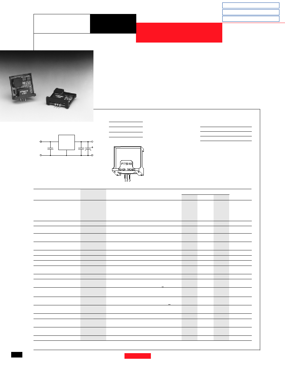
Standard Application
C
1
= Optional ceramic (1-5µF)
C
2
= Optional ceramic (1-5µF)
C
3
= Required Electrolytic (100µF)
V
IN
(+)
COM
PT5040
1
2
3
COM
V
OUT
(+)
C1
C2
C3
NOTE: Boost Topology ISRs are not Short-Circuit Protected.
∑
Wide Input Voltage Range
∑
85% Efficiency
∑
Internal Over-Temperature
Protection
∑
Laser-trimmed Output Voltage
∑
Soft Start
The Power Trends' PT5040 Series
is a 3-terminal Integrated Switching
Regulator (ISR) designed for use with
+5 volt systems that require an addi-
tional regulated +8 to +20 volts with up
to 1A of output current. These ISRs
are packaged in the 3 pin SIP configu-
ration.
1 AMP STEP-UP
INTEGRATED SWITCHING REGULATOR
P T 5 0 4 0
S e r i e s
Pin
Function
1
V
in
2
GND
3
V
out
Pkg Style 100
Specifications
Characteristics
PT5040 SERIES
(T
a
=25
∞C unless noted)
Symbols
Conditions
Min
Typ
Max
Units
Output Current
I
o
Over V
in
range
V
o
=20V
0.1*
--
0.5
A
V
o
=18V
0.1*
--
0.6
A
V
o
=12V
0.1*
--
1.0
A
V
o
=15V
0.1*
--
0.75
A
V
o
=8V
0.1*
--
1.5
A
V
o
=9V
0.1*
--
1.25
A
Current Limit**
I
cl
V
in
= +5V
--
1.5 I
o
max
--
A
Inrush Current
I
ir
V
in
= +5V @ max I
o
--
2.5
--
A
t
ir
On start up
--
1
--
mSec
Input Voltage Range
V
in
I
o
= 0.1 to I
o
max
4.75
--
(V
o-
1V)
V
PT5047/5049
4.75
--
14
V
Output Voltage Tolerance
V
o
Over V
in
Range
I
o
= I
max,
T
a
= -20∞C to shutdown
--
±1.5
±3.0
%V
o
Line Regulation
Reg
line
Over V
in
range
--
±0.5
±1.0
%V
o
Load Regulation
Reg
load
0.1
I
o
I
o
max
--
±0.5
±1.0
%V
o
V
o
Ripple/Noise
V
n
V
in
= +5V, I
o
=I
o
max
--
±2
±5
%V
o
Transient Response
t
tr
25% load change
--
500
--
µSec
V
os
V
o
over/undershoot
--
3.0
5.0
%V
o
Efficiency
V
in
= +5V, I
o
=0.5A, V
o
= +12V
--
85
--
%
Switching Frequency
o
Over V
in
and I
o
ranges
V
o
<15V
500
650
800
kHz
V
o
>15V
650
800
950
kHz
Absolute Maximum
T
a
--
-20
--
+85
∞C
Operating Temperature Range
Recommended Operating
T
a
Free Air Convection, (40-60LFM) V
o
<15V
-20
--
70***
∞C
Temperature Range
Over V
in
and I
o
ranges
V
o
>15V
-20
--
55***
∞C
Thermal Resistance
ja
Free Air Convection
--
40
--
∞C/W
(40-60LFM)
Storage Temperature
T
s
-40
--
+125
∞C
Mechanical Shock
Per Mil-STD-883D, Method 2002.3
1 msec, Half Sine, mounted to a fixture
--
500
--
G's
Mechanical Vibration
Per Mil-STD-883D, Method 2007.2,
--
5
--
G's
20-2000 Hz, Soldered in a PC Board
Weight
--
4.5
--
grams
* ISR will operate down to no load with reduced specifications.
** Boost topology ISRs are not short circuit protected. *** See SOA Curves.
Revised 6/30/98
For assistance or to order, call
(800) 531-5782
Power Trends, Inc.
27715 Diehl Road, Warrenville, IL 60555
(800) 531-5782
Fax: (630) 393-6902 http://www.powertrends.com
45
5V to 3.x Converters
5V Bus Products
DA
T
A
SHEETS
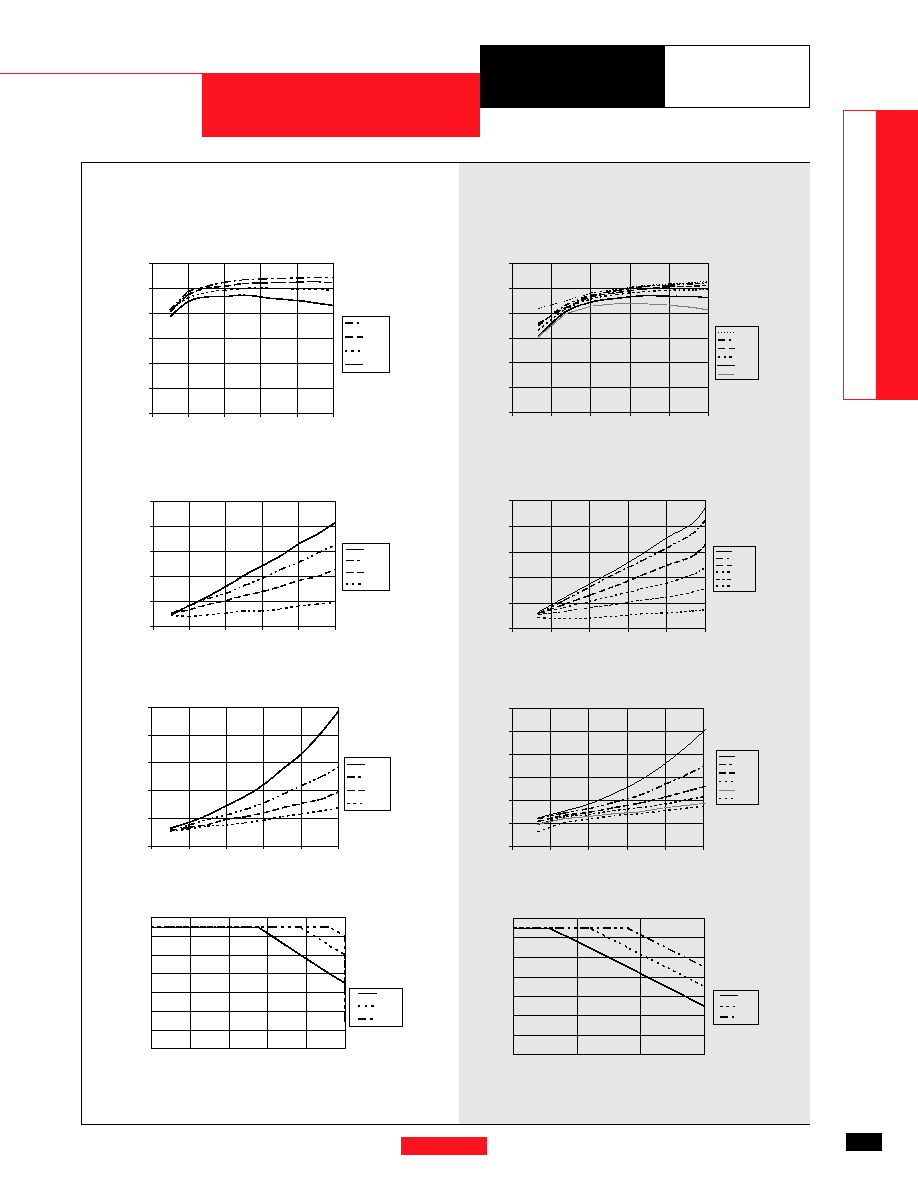
C H A R A C T E R I S T I C D A T A
PT5041, +12.0 VDC
(See Note 1)
PT5042, +15.0 VDC
(See Note 1)
Note 1:
All data listed in the above graphs has been developed from actual products tested at 25∞C. This data is considered typical data for the ISR.
P T 5 0 4 0
S e r i e s
Efficiency vs Output Current
Ripple Voltage vs Output Current
Power Dissipation vs Output Current
Efficiency vs Output Current
Ripple Voltage vs Output Current
Power Dissipation vs Output Current
Safe Operating Area (V
IN
=5V)
Safe Operating Area (V
IN
=5V)
Efficiency - %
Ripple-(mV)
PD-(W
atts)
Iout-(Amps)
Iout-(Amps)
PD-(W
atts)
Ripple-(mV)
Iout-(Amps)
Iout-(Amps)
Ambient T
e
mperatur
e
- (C∞)
Ambient T
e
mperatur
e
- (C∞)
Maximum Output Current - (Amps)
Maximum Output Current - (Amps)
Iout-(Amps)
Iout-(Amps)
4 0
5 0
6 0
7 0
8 0
9 0
10 0
0
0 .2
0 .4
0 .6
0 .8
1
11.0V
8.0V
6.0V
5.0V
V in
0
0.5
1
1.5
2
2.5
0
0.2
0.4
0.6
0.8
1
5 .0 V
6 .0 V
8 .0 V
1 1 .0 V
V in
0
5 0
10 0
15 0
20 0
25 0
0
0 .2
0 .4
0 .6
0 .8
1
5 .0 V
6 .0 V
8 .0 V
1 1 .0 V
V in
4 0
5 0
6 0
7 0
8 0
9 0
10 0
0
0.1 5
0 .3
0.4 5
0 .6
0.7 5
14.0V
12.0V
10.0V
8.0V
6.0V
5.0V
V in
0
0.5
1
1.5
2
2.5
3
0
0.15
0.3
0.45
0.6
0.75
5.0V
6.0V
8.0V
10.0V
12.0V
14.0V
Vin
0
5 0
10 0
15 0
20 0
25 0
0
0.1 5
0 .3
0.4 5
0 .6
0.7 5
5.0 V
6.0 V
8.0 V
10 .0V
12 .0V
14 .0V
V in
Efficiency - %
20
30
40
50
60
70
80
90
0.00
0.25
0.50
0.75
0 LFM
60 LFM
90 LFM
Airflow
20
30
40
50
60
70
80
90
0
0.2
0.4
0.6
0.8
1
0 LFM
60 LFM
90 LFM
Airflow

IMPORTANT NOTICE
Texas Instruments and its subsidiaries (TI) reserve the right to make changes to their products or to discontinue
any product or service without notice, and advise customers to obtain the latest version of relevant information
to verify, before placing orders, that information being relied on is current and complete. All products are sold
subject to the terms and conditions of sale supplied at the time of order acknowledgement, including those
pertaining to warranty, patent infringement, and limitation of liability.
TI warrants performance of its semiconductor products to the specifications applicable at the time of sale in
accordance with TI's standard warranty. Testing and other quality control techniques are utilized to the extent
TI deems necessary to support this warranty. Specific testing of all parameters of each device is not necessarily
performed, except those mandated by government requirements.
CERTAIN APPLICATIONS USING SEMICONDUCTOR PRODUCTS MAY INVOLVE POTENTIAL RISKS OF
DEATH, PERSONAL INJURY, OR SEVERE PROPERTY OR ENVIRONMENTAL DAMAGE ("CRITICAL
APPLICATIONS"). TI SEMICONDUCTOR PRODUCTS ARE NOT DESIGNED, AUTHORIZED, OR
WARRANTED TO BE SUITABLE FOR USE IN LIFE-SUPPORT DEVICES OR SYSTEMS OR OTHER
CRITICAL APPLICATIONS. INCLUSION OF TI PRODUCTS IN SUCH APPLICATIONS IS UNDERSTOOD TO
BE FULLY AT THE CUSTOMER'S RISK.
In order to minimize risks associated with the customer's applications, adequate design and operating
safeguards must be provided by the customer to minimize inherent or procedural hazards.
TI assumes no liability for applications assistance or customer product design. TI does not warrant or represent
that any license, either express or implied, is granted under any patent right, copyright, mask work right, or other
intellectual property right of TI covering or relating to any combination, machine, or process in which such
semiconductor products or services might be or are used. TI's publication of information regarding any third
party's products or services does not constitute TI's approval, warranty or endorsement thereof.
Copyright
©
1999, Texas Instruments Incorporated