 | –≠–ª–µ–∫—Ç—Ä–æ–Ω–Ω—ã–π –∫–æ–º–ø–æ–Ω–µ–Ω—Ç: PT5044LT | –°–∫–∞—á–∞—Ç—å:  PDF PDF  ZIP ZIP |

For technical support and more information, see inside back cover or visit www.ti.com
Ordering Information
PT5041
o = +12 Volts
PT5042
o = +15 Volts
PT5044
o = +8 Volts
PT5045
o = +9 Volts
PT5046
o = +10 Volts
PT5047
o = +18 Volts
PT5048
o = +12.6 Volts
PT5049
o = +20 Volts
Pin-Out Information
Standard Application
C
1
= Optional ceramic (1-5µF)
C
2
= Optional ceramic (1-5µF)
C
3
= Required Electrolytic (100µF)
NOTE: Boost Topology ISRs are not Short-Circuit Protected.
Features
∑
Wide Input Voltage Range
∑
85% Efficiency
∑
Internal Over-Temperature
Protection
∑
Laser-trimmed Output Voltage
∑
Soft Start
∑
5-Pin Mount Option
(Suffixes L & M)
1-A Positive Step-up
Integrated Switching Regulator
PT5040 Series
Pin
Function
1
V
in
2
GND
3
V
out
SLTS026B
(Revised 12/19/2001)
PT Series Suffix
(PT1234
x
)
Case/Pin
Order
Package
Configuration
Suffix
Code *
Vertical
N
(EAD)
Horizontal
A
(EAA)
SMD
C
(EAC)
Horizontal, 2-pin Tab
M
(EAM)
SMD, 2-Pin Tab
L
(EAL)
* Previously known as package styles 100/110.
(Reference the applicable package code drawing
for the dimensions and PC board layout)
Description
The PT5040 is a series of 3-pin
boost-voltage Integrated Switching
Regulators (ISRs). These ISRs are
designed for use with +5V bus systems
that require an additional regulated
+8V to +20V with up to 1A of output
current. These ISRs are packaged in
the 3-pin, single in-line pin (SIP)
package configuration.
Specifications
(Unless otherwise stated, T
a
=25∞C, V
in
=5V, I
o
=I
o
max, C
3
=100µF)
PT5040 SERIES
Characteristics
Symbol
Conditions
Min
Typ
Max
Units
Output Current
I
o
Over V
in
range
PT5049
0.1
(1)
--
0.5
PT5047
0.1
(1)
--
0.6
PT5041/48
0.1
(1)
--
1.0
A
PT5042
0.1
(1)
--
0.75
PT5044
0.1
(1)
--
1.5
PT5045/46
0.1
(1)
--
1.2
Input Voltage Range
V
in
Over Io range
4.75
--
(V
o
≠
1)
V
PT5047/5049
4.75
--
14
Output Voltage Tolerance
V
o
Over V
in
Range
T
a
= -20∞C to SOA derating limit
(3)
--
±1.5
±3.0
%V
o
Line Regulation
Reg
line
Over V
in
range
--
±0.5
±1.0
%V
o
Load Regulation
Reg
load
I
o
min
I
o
I
o
max
--
±0.5
±1.0
%V
o
Efficiency
I
o
=0.5A
--
85
--
%
V
o
Ripple (pk-pk)
V
r
20MHz bandwidth
--
±2
±5
%V
o
Transient Response
t
tr
25% load change
--
500
--
µSec
V
os
V
o
over/undershoot
--
3.0
5.0
%V
o
Current Limit
I
lim
--
150
(2)
--
%I
o
max
Inrush Current
I
ir
On start up
--
5.5
(3)
--
A
t
ir
--
1
--
mSec
Switching Frequency
s
Over V
in
and I
o
ranges
V
o
<15V
500
650
800
kHz
V
o
>15V
650
800
950
Operating Temperature Range
T
a
--
-20
--
+85
(4)
∞C
Thermal Resistance
ja
Free Air Convection
--
40
--
∞C/W
(40-60LFM)
Storage Temperature
T
s
-40
--
+125
∞C
Mechanical Shock
Per Mil-STD-883D, Method 2002.3
1 msec, Half Sine, mounted to a fixture
--
500
--
G's
Mechanical Vibration
Suffixes N, A, & C
--
5
--
G's
Per Mil-STD-883D, 20-2000 Hz
Suffixes L & M
--
20
(5)
--
Weight
Suffixes N, A, & C
--
4.5
--
grams
Suffixes L & M
--
6.5
--
Notes:
(1) The ISR will operate at no load with reduced specifications.
(2) Boost topology ISRs are not short circuit protected.
(3) The inrush current stated is above the normal input current for the associated output load.
(4) See Safe Operating Area curves or consult the factory for the appropriate derating
(5) The tab pins on the 5-pin mount package types (suffixes L & M) must be soldered. For more information see the applicable package outline drawing.
P T 5 0 4 0
3
2
1
C
3
100µF
+
C
2
+V
out
COM
COM
+V
in
C
1
For technical support and more information, see inside back cover or visit www.ti.com
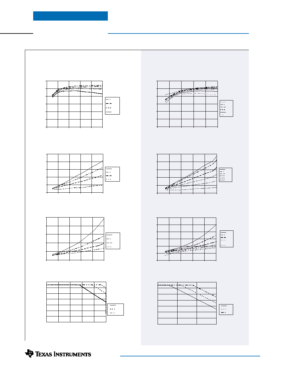
Typical Characteristics
PT5041, +12.0 VDC
(See Note A)
PT5042, +15.0 VDC
(See Note A)
Efficiency vs Output Current
Ripple Voltage vs Output Current
Power Dissipation vs Output Current
Efficiency vs Output Current
Ripple Voltage vs Output Current
Power Dissipation vs Output Current
Safe Operating Area (V
IN
=5V)
(See Note B)
Safe Operating Area (V
IN
=5V)
(See Note B)
Efficiency - %
Ripple-(mV)
PD-(W
atts)
Iout-(Amps)
Iout-(Amps)
PD-(W
atts)
Ripple-(mV)
Iout-(Amps)
Iout-(Amps)
Ambient T
emperature - (C∞)
Ambient T
emperature - (C∞)
Maximum Output Current - (Amps)
Maximum Output Current - (Amps)
Iout-(Amps)
Iout-(Amps)
4 0
5 0
6 0
7 0
8 0
9 0
1 0 0
0
0 .2
0 .4
0 .6
0 .8
1
11.0V
8.0V
6.0V
5.0V
V in
0
0.5
1
1.5
2
2.5
0
0.2
0.4
0.6
0.8
1
5.0V
6.0V
8.0V
11.0V
Vin
0
5 0
1 0 0
1 5 0
2 0 0
2 5 0
0
0 .2
0 .4
0 .6
0 .8
1
5.0V
6.0V
8.0V
11.0V
V in
4 0
5 0
6 0
7 0
8 0
9 0
10 0
0
0.1 5
0 .3
0.4 5
0 .6
0.7 5
14.0V
12.0V
10.0V
8.0V
6.0V
5.0V
V in
0
0.5
1
1.5
2
2.5
3
0
0.15
0.3
0.45
0.6
0.75
5.0V
6.0V
8.0V
10.0V
12.0V
14.0V
Vin
0
5 0
100
150
200
250
0
0.15
0 .3
0.45
0 .6
0.75
5 . 0 V
6 . 0 V
8 . 0 V
1 0 . 0 V
1 2 . 0 V
1 4 . 0 V
V in
Efficiency - %
20
30
40
50
60
70
80
90
0. 00
0. 25
0. 50
0. 75
0 LFM
60 LFM
90 LFM
Airflow
20
30
40
50
60
70
80
90
0
0.2
0.4
0.6
0.8
1
0 LFM
60 LFM
90 LFM
Airflow
1-A Positive Step-up
Integrated Switching Regulator
PT5040 Series
Note A:
Characteristic data has been developed from actual products tested at 25∞C. This data is considered typical data for the Converter.
Note B:
Thermal derating graphs are developed in free-air convection cooling, which corresponds to approximately 40≠60LFM of airflow.

IMPORTANT NOTICE
Texas Instruments Incorporated and its subsidiaries (TI) reserve the right to make corrections, modifications,
enhancements, improvements, and other changes to its products and services at any time and to discontinue
any product or service without notice. Customers should obtain the latest relevant information before placing
orders and should verify that such information is current and complete. All products are sold subject to TI's terms
and conditions of sale supplied at the time of order acknowledgment.
TI warrants performance of its hardware products to the specifications applicable at the time of sale in
accordance with TI's standard warranty. Testing and other quality control techniques are used to the extent TI
deems necessary to support this warranty. Except where mandated by government requirements, testing of all
parameters of each product is not necessarily performed.
TI assumes no liability for applications assistance or customer product design. Customers are responsible for
their products and applications using TI components. To minimize the risks associated with customer products
and applications, customers should provide adequate design and operating safeguards.
TI does not warrant or represent that any license, either express or implied, is granted under any TI patent right,
copyright, mask work right, or other TI intellectual property right relating to any combination, machine, or process
in which TI products or services are used. Information published by TI regarding third≠party products or services
does not constitute a license from TI to use such products or services or a warranty or endorsement thereof.
Use of such information may require a license from a third party under the patents or other intellectual property
of the third party, or a license from TI under the patents or other intellectual property of TI.
Reproduction of information in TI data books or data sheets is permissible only if reproduction is without
alteration and is accompanied by all associated warranties, conditions, limitations, and notices. Reproduction
of this information with alteration is an unfair and deceptive business practice. TI is not responsible or liable for
such altered documentation.
Resale of TI products or services with statements different from or beyond the parameters stated by TI for that
product or service voids all express and any implied warranties for the associated TI product or service and
is an unfair and deceptive business practice. TI is not responsible or liable for any such statements.
Mailing Address:
Texas Instruments
Post Office Box 655303
Dallas, Texas 75265
Copyright
2001, Texas Instruments Incorporated