 | –≠–ª–µ–∫—Ç—Ä–æ–Ω–Ω—ã–π –∫–æ–º–ø–æ–Ω–µ–Ω—Ç: PT5071 | –°–∫–∞—á–∞—Ç—å:  PDF PDF  ZIP ZIP |

For technical support and more information, see inside back cover or visit www.ti.com/powertrends
PT5071--12V
1.5 Amp, 12V Step-Up/Step-Down
Integrated Switching Regulator
SLTS139
(Revised 2/7/2001)
Standard Application
C
1
, C
2
= Required 100µF electrolytic (See footnotes)
Ordering Information
PT5071
® = +12 Volts
PT Series Suffix
(PT1234
X
)
Case/Pin
Configuration
Vertical Through-Hole
N
Horizontal Through-Hole
A
Horizontal Surface Mount
C
Pin
Function
1
N/C
2
UVLO Adj
3
STBY*
4
V
in
5
V
in
6
V
in
7
GND
8
GND
9
GND
10
GND
11
V
out
12
V
out
13
V
out
14
V
out
Adjust
Features
∑
Single-Device:
+12V Output, 7-16V Input
∑
84% Efficiency
∑
14-Pin ExcaliburTM Package
∑
Output Current Limit
∑
Adjustable Output Voltage
∑
Adjustable Undervoltage Lockout
∑
Solderable Copper Case
Description
The PT5071 is a 1.5-ampere rated step-up/
step-down Integrated Switching Regulator
(ISR) that provides a tightly regulated 12V
output voltage from a 7V to 16V variable
input source. This high-performance ISR has
applications in systems where the input
voltage straddles the desired 12V output.
The regulator has an adjustable output
voltage and input start-up threshold, and a
standby function for power conservation.
Pin-Out Information
C
1
+
C
2
+
PT5071
UVadj
G N D
V
IN
V
OUT
V
0
adj
STBY*
4-6
11-13
2
3
7-10
14
V
I N
V
O U T
S T B Y
G N D
G N D
U V
A D J
(For dimensions and PC board layout,
see Package Styles 1360 and 1370.)
For Inhibit pin:
Open = output enabled
Ground = output disabled
Specifications
Characteristics
PT5071
(T
a
= 25∞C unless noted)
Symbols
Conditions
Min
Typ
Max
Units
Output Current
I
o
Over V
in
Range
0.1
(1)
--
1.5
A
Current Limit
I
lim
V
in
= 12V
--
4.0
A
Input Voltage Range
V
in
0.1A
I
o
I
o
max
7.0
--
16.0
V
Output Voltage Tolerance
V
o
V
in
=12V, I
o
=I
o
max
±1.0
%
≠40∞C
T
a
+85∞C
Output Voltage Adjust Range
V
o
adj
10
--
15
V
Line Regulation
Reg
line
Over V
in
Range, I
o
=I
o
max
--
±0.5
%
Load Regulation
Reg
load
V
in
=12V, 0.1
I
o
I
o
max
--
±0.5
%
Vo Ripple/Noise
V
n
V
in
=12V, I
o
=I
o
max
--
±2.0
±3.0
%
Transient Response
t
tr
Load step from 50% to 100% I
o
max, V
in
=12V
--
200
--
µSec
with C
2
= 100µF
V
os
V
o
over/undershoot
--
1.0
--
%V
o
Efficiency
V
in
=12V, V
o
=12V, I
o
=1.5A
--
83
--
%
Switching Frequency
o
Over V
in
Range
--
550
--
kHz
0.1A
I
o
I
o
max
Absolute Maximum
T
a
Over V
in
range
≠40
(2)
--
+85
(3)
∞C
Operating Temperature Range
Storage Temperature
T
s
--
≠40
--
+125
∞C
Mechanical Shock
Per Mil-STD-883D, Method 2002.3 , 1 msec,
--
TBD
--
G's
Half Sine, mounted to a fixture
Mechanical Vibration
Per Mil-STD-883D, Method 2007.2,
20-2000 Hz, Soldered in a PC board
--
TBD
--
G's
Weight
--
--
--
25
--
grams
Notes: 1. The regulator will operate down to no load with reduced specifications.
2. For operating temperatures below 0∞C, it is recommended that tantalum capacitors be used at both the input and output.
3. See SOA curves, or contact the factory for derating guidelines.
Input/Output Capacitors: The PT5071 regulator requires a 100µF electrolytic capacitor at the input and output for proper operation in all applications. The ESR
(equivalent series resistance) of both capacitors must be less than 250m
@100kHz. In addition, C
1
and C
2
must be rated to a minimum of 300mArms ripple current.
For technical support and more information, see inside back cover or visit www.ti.com/powertrends
For technical support and more information, see inside back cover or visit www.ti.com/powertrends
For technical support and more information, see inside back cover or visit www.ti.com/powertrends
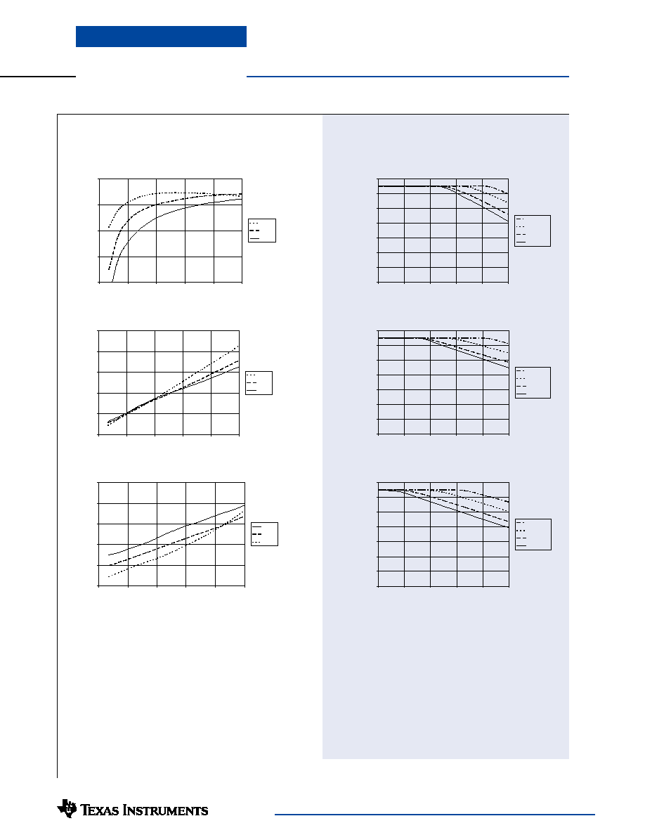
Typical Characteristics
Note A:
All Characteristic data in the above graphs has been developed from actual products tested at 25∞C. This data is considered typical data for the ISR.
Note B:
SOA curves represent operating conditions at which internal components are at or below manufacturer's maximum rated operating temperatures.
PT5071--12V
1.5 Amp, 12V Step-Up/Step-Down
Integrated Switching Regulator
20.0
30.0
40.0
50.0
60.0
70.0
80.0
90.0
0.0
0.3
0.6
0.9
1.2
1.5
Iout (A)
Ambient Temperature (∞C)
200LFM
120LFM
60LFM
Nat conv
Airflow
20.0
30.0
40.0
50.0
60.0
70.0
80.0
90.0
0.0
0.3
0.6
0.9
1.2
1.5
Iout (A)
Ambient Temperature (∞C)
200LFM
120LFM
60LFM
Nat conv
Airflow
20.0
30.0
40.0
50.0
60.0
70.0
80.0
90.0
0.0
0.3
0.6
0.9
1.2
1.5
Iout (A)
Ambient Temperature (∞C)
200LFM
120LFM
60LFM
Nat conv
Airflow
Safe Operating Area Curves
(See Note B)
PT5071, V
in
=7V
PT5071, V
in
=12V
PT5071, V
in
=16V
0
50
100
150
200
250
0
0.3
0.6
0.9
1.2
1.5
Iout (A)
Ripple - mV
7.0V
12.0V
16.0V
V
IN
50
60
70
80
90
0
0.3
0.6
0.9
1.2
1.5
Iout (A)
Efficiency - %
7.0V
12.0V
16.0V
V
IN
0
1
2
3
4
5
0
0.3
0.6
0.9
1.2
1.5
Iout (A)
Pd - Watts
16.0V
12.0V
7.0V
V
IN
PT5071 Performance, V
o
=12V
(See Note A)
Efficiency vs Output Current
Ripple vs Output Current
Power Dissipation vs Output Current

IMPORTANT NOTICE
Texas Instruments and its subsidiaries (TI) reserve the right to make changes to their products or to discontinue
any product or service without notice, and advise customers to obtain the latest version of relevant information
to verify, before placing orders, that information being relied on is current and complete. All products are sold
subject to the terms and conditions of sale supplied at the time of order acknowledgment, including those
pertaining to warranty, patent infringement, and limitation of liability.
TI warrants performance of its products to the specifications applicable at the time of sale in accordance with
TI's standard warranty. Testing and other quality control techniques are utilized to the extent TI deems necessary
to support this warranty. Specific testing of all parameters of each device is not necessarily performed, except
those mandated by government requirements.
Customers are responsible for their applications using TI components.
In order to minimize risks associated with the customer's applications, adequate design and operating
safeguards must be provided by the customer to minimize inherent or procedural hazards.
TI assumes no liability for applications assistance or customer product design. TI does not warrant or represent
that any license, either express or implied, is granted under any patent right, copyright, mask work right, or other
intellectual property right of TI covering or relating to any combination, machine, or process in which such
products or services might be or are used. TI's publication of information regarding any third party's products
or services does not constitute TI's approval, license, warranty or endorsement thereof.
Reproduction of information in TI data books or data sheets is permissible only if reproduction is without
alteration and is accompanied by all associated warranties, conditions, limitations and notices. Representation
or reproduction of this information with alteration voids all warranties provided for an associated TI product or
service, is an unfair and deceptive business practice, and TI is not responsible nor liable for any such use.
Resale of TI's products or services with
statements different from or beyond the parameters stated by TI for
that product or service voids all express and any implied warranties for the associated TI product or service,
is an unfair and deceptive business practice, and TI is not responsible nor liable for any such use.
Also see: Standard Terms and Conditions of Sale for Semiconductor Products. www.ti.com/sc/docs/stdterms.htm
Mailing Address:
Texas Instruments
Post Office Box 655303
Dallas, Texas 75265
Copyright
©
2001, Texas Instruments Incorporated