 | –≠–ª–µ–∫—Ç—Ä–æ–Ω–Ω—ã–π –∫–æ–º–ø–æ–Ω–µ–Ω—Ç: PT5806A | –°–∫–∞—á–∞—Ç—å:  PDF PDF  ZIP ZIP |
For technical support and more information, see inside back cover or visit www.ti.com
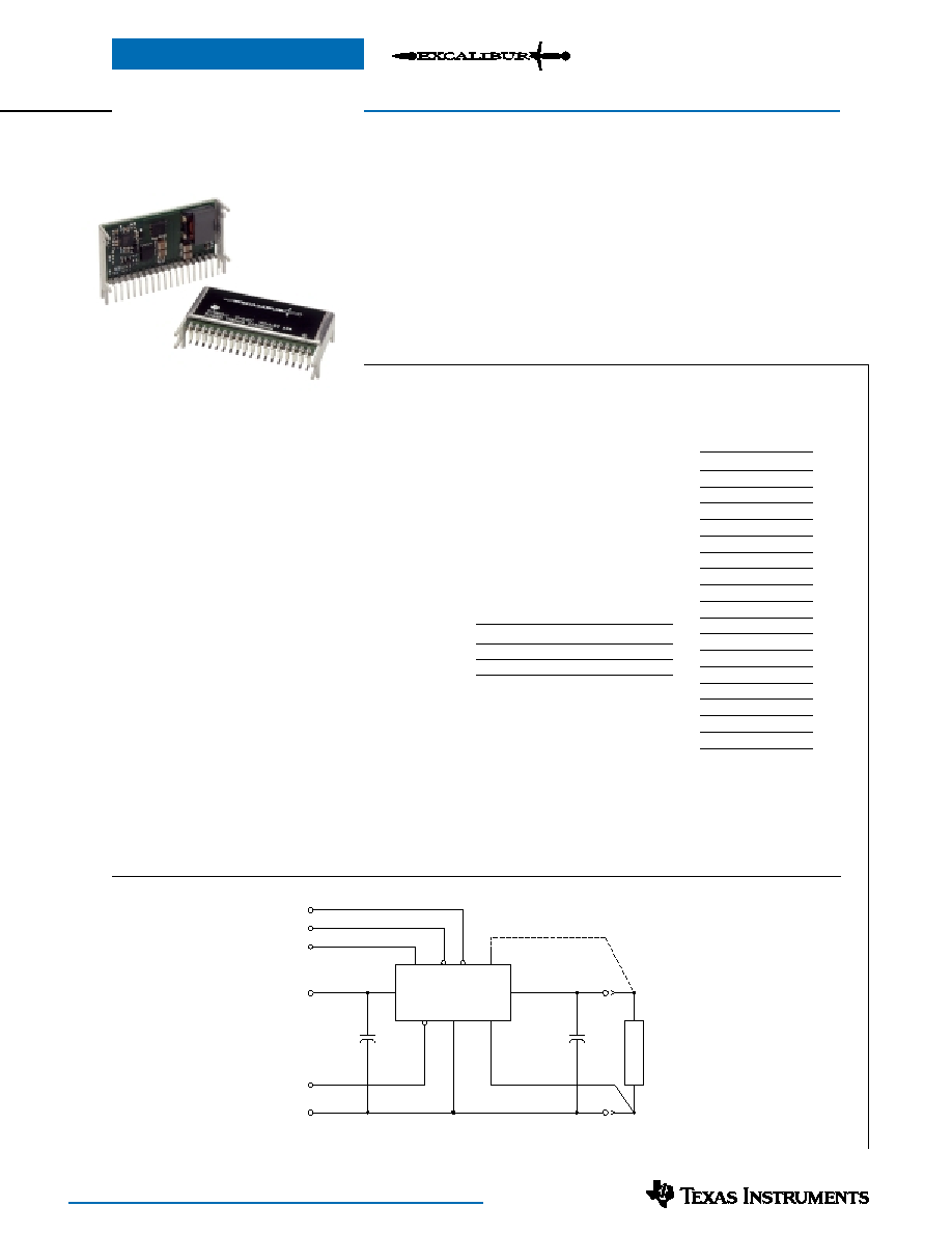
PT5800 Series
18-A 5-V Input Adjustable
Integrated Switching Regulator
SLTS171A JANUARY 2003 - REVISED - MARCH 2003
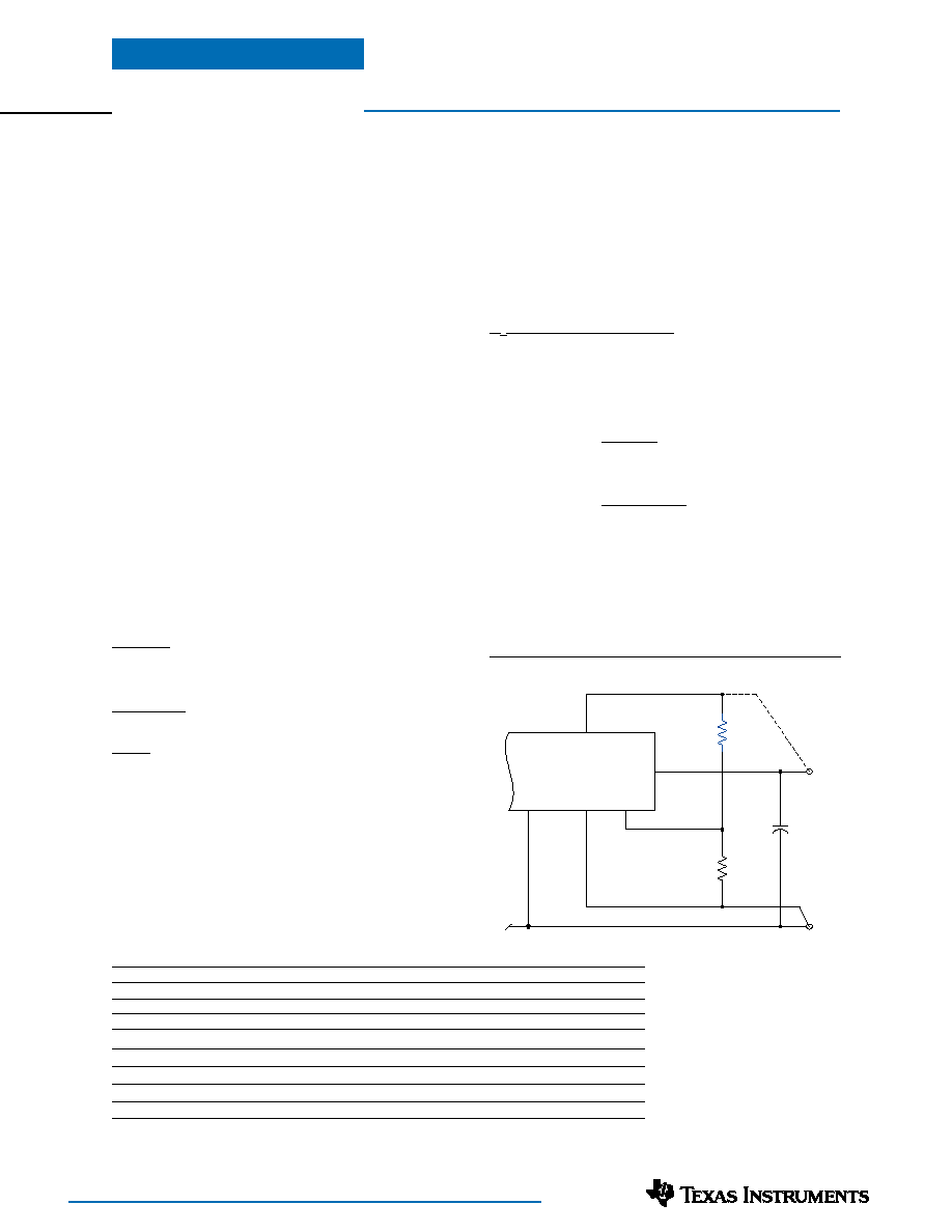
Standard Application
C
in
= Required 820µF
C
out
= Required 330µF
Ordering Information
PT5801
H = 3.3 Volts
PT5802
H = 2.5 Volts
PT5803
H = 1.8 Volts
PT5804
H = 1.5 Volts
PT5805
H = 1.2 Volts
PT5806
H = 1.0 Volts
Pin
Function
1
V
o
Adjust
2
Inhibit*
3
Margin Dn*
4
Margin Up*
5
V
in
6
V
in
7
V
in
8
Sense(≠)
9
GND
10
GND
11
GND
12
GND
13
GND
14
V
out
15
V
out
16
V
out
17
V
out
18
Sense(+)
Features
∑
5V Input
∑
18A Output Current
∑
DSP Compatible
∑
Low-Profile (8mm)
∑
>90% Efficiency
∑
Output Margin Control (±5%)
∑
Adjustable Output Voltage
∑
On/Off Inhibit Function
∑
Pre-Bias Startup Capability
Pin-Out Information
* Denotes negative logic:
Open = Normal operation
Ground = Function active
Description
The PT5800 ExcaliburTM series of integrated
switching regulators (ISRs) combines outstand-
ing power density with a comprehensive list of
features. They are an ideal choice for applications
where board space is a premium and performance
cannot be compromised. These modules provide
18A of output current, yet are housed in a low-
profile, 18-pin package that is almost half the
size of the previous product generation. The
integral copper case construction requires no
heatsink, and offers the advantages of solderabil-
ity and a small footprint (0.736 in≤ for suffix `N').
Both through-hole and surface mount pin con-
figurations are available.
The PT5800 series operates from a 5-V input
bus and provides a convenient point-of-load power
source for the industry's latest high-performance
DSPs and microprocessors. The series includes
output voltage options as low as 1.0VDC.
Other features include external output voltage
adjustment, a ±5% margin control, on/off inhibit,
short circuit protection, thermal shutdown, and a
differential remote sense.
PT Series Suffix
(PT1234
x
)
Case/Pin
Order
Package
Configuration
Suffix
Code
Vertical
N
(EPP)
Horizontal
A
(EPQ)
SMD
C
(EPS)
(Reference the applicable package code draw-
ing for the dimensions and PC board layout)
∑
Over-Current Protection
∑
Over-Temperature Protection
∑
Small Footprint
(0.736 in≤, Suffix `N')
∑
Surface Mount Compatible
∑
IPC Lead Free 2
PT5800
V
o
Adjust
Margin Up
Margin Dn
V
IN
9≠13
4
1
18
14≠17
5, 6, 7
8
2
L
O
A
D
C
IN
820µF
(Required)
+
C
OUT
330µF
(Required)
+
Inhibit
GND
GND
V
OUT
3
Sense(+)
Sense(≠)

For technical support and more information, see inside back cover or visit www.ti.com
PT5800 Series
18-A 5-V Input Adjustable
Integrated Switching Regulator
Specifications
(Unless otherwise stated, T
a
=25∞C, V
in
=5V, C
in
=820µF, C
out
=330µF, and I
o
=I
o
max)
PT5800 SERIES
Characteristics
Symbols
Conditions
Min
Typ
Max
Units
Output Current
I
o
V
in
=5V
0
--
18
A
Input Voltage Range
V
in
Over I
o
range
4.5
--
5.5
V
Set-Point Voltage Tolerance
V
o
tol
--
--
±2
%V
o
Temperature Variation
Reg
temp
≠40∞C <T
a
< +85∞C
--
±0.5
--
%V
o
Line Regulation
Reg
line
Over V
in
range
--
±8
--
mV
Load Regulation
Reg
load
Over I
o
range
--
±5
--
mV
Total Output Variation
Reg
tot
Includes set-point, line, load,
--
--
±3
%V
o
≠40∞C
T
a
+85∞C
Efficiency
I
o
=12A
PT5801 (3.3V)
--
94
--
PT5802 (2.5V)
--
92
--
PT5803 (1.8V)
--
90
--
%
PT5804 (1.5V)
--
88
--
PT5805 (1.2V)
--
86
--
PT5806 (1.0V)
--
84
--
V
o
Ripple (pk-pk)
V
r
20MHz bandwidth
--
20
--
mVpp
Transient Response
1A/µs load step, 50 to 100% I
o
max,
t
tr
Recovery Time
--
50
--
µSec
V
tr
V
o
over/undershoot
--
100
--
mV
Over-Current Threshold
I
TRIP
Reset, followed by auto-recovery
--
30
--
A
Output Voltage Adjust
V
o
adj
With V
o
Adjust
--
±15
(1)
--
%
With Margin Up/Dn
--
±5
--
Switching Frequency
s
Over V
in
and I
o
ranges
250
300
350
kHz
Inhibit Control (pin 2)
Referenced to GND (pins 9≠13)
Input High Voltage
V
IH
V
in
≠0.5
--
Open
(2)
V
Input Low Voltage
V
IL
≠0.2
--
0.8
Input Low Current
I
IL
Pin 2 to GND
--
≠10
--
µA
Standby Input Current
I
in
standby
Pin 2 to GND
--
5
--
mA
External Input Capacitance
C
in
820
(3)
--
--
µF
External Output Capacitance
C
out
330
(4)
--
5,000
µF
Operating Temperature Range
T
a
Over V
in
range
≠40
(4)
--
85
(5)
∞C
Over-Temperature Protection
OTP
Measured at center of case, auto-reset
--
110
--
∞C
Solder Reflow Temperature
T
reflow
Surface temprature of module pins or case
--
--
215
(6)
∞C
Storage Temperature
T
s
--
≠40
--
125
∞C
Reliability
MTBF
Per Bellcore TR-332
5.8
--
--
10
6
Hrs
50% stress, T
a
=40∞C, ground benign
Mechanical Shock
Mil-STD-883D, Method 2002.3
--
500
--
G
Half Sine, mounted to a fixture
Mechanical Vibration
Mil-STD-883D, Method 2007.2,
Suffix N
--
20
(7)
--
G
20-2000 Hz, PCB mounted
Suffixes A, C
--
20
(7)
--
Weight
--
--
--
20
--
grams
Flammability
--
Materials meet UL 94V-0
Notes: (1) This is a typical value. For the adjustment limits of a specific model consult the related application note on output voltage adjustment.
(2) The Inhibit control (pin 2) has an internal pull-up to V
in
, and if left open-circuit the module will operate when input power is applied. A small low-
leakage (<100nA) MOSFET is recommended to control this input. See application notes for more information.
(3) An 820µF electrolytic input capacitor is required for proper operation. This capacitor must be rated for a minimumm of 0.7 Arms of ripple current.
(4) For operation below 0∞C, C
OUT
must have stable characteristics. Use either low-ESR tantalum or OsconÆ type capacitors.
(5) See SOA curves or consult factory for the appropriate derating.
(6) During solder reflow of SMD package version do not elevate the module case, pins, or internal component temperatures above a peak of 215∞C. For
further guidance refer to the application note, "Reflow Soldering Requirements for Plug-in Power Surface Mount Products," (SLTA051)
(7) The case pins on the through-hole package types (suffixes N & A) must be soldered. For more information see the applicable package outline drawing.
SLTS171A JANUARY 2003 - REVISED - MARCH 2003

For technical support and more information, see inside back cover or visit www.ti.com
Note A:
Characteristic data has been developed from actual products tested at 25∞C. This data is considered typical data for the ISR.
Note B:
SOA curves represent operating conditions at which internal components are at or below manufacturer's maximum rated operating temperatures.
Efficiency vs Output Current
Power Dissipation vs Output Current
Performance Data; V
in
=5V
(See Note A)
Output Ripple vs Output Current
PT5800 Series
18-A 5-V Input Adjustable
Integrated Switching Regulator
Pin Descriptions
Vin:
The positive supply voltage input for the module
with respect to the common ground (GND).
Vout:
This is the regulated output voltage from the mod-
ule with respect to the common ground (GND).
GND:
The common ground node to which the input,
output, and external control signals are referenced.
Sense(≠):
Provides the regulator with the ability to sense
the set-point voltage directly across the load. For opti-
mum output voltage accuracy this pin should always be
connected to GND, even for applications that demand a
relatively light load.
Sense(+):
When used with Sense(≠), the regulation circuitry
will compensate for voltage drop between the converter
and the load. The pin may be left open circuit, but con-
necting it to V
out
will optimize load regulation.
Inhibit*:
This is an open-collector (open-drain) negative
logic input, referenced to GND. Pulling this pin to
GND disables the module's output voltage. If Inhibit* is
left open circuit, the output will be active whenever a
valid input source is applied.
V
o
Adjust:
This pin is used to trim the output voltage
over a typical range of ±15% of nominal. The adjust-
ment method uses an external resistor. The resistor is
connected from V
o
Adjust to either the (-)Sense or (+)Sense,
in order to adjust the output either up or down, respec-
tively. Consult the related application note for the adjust
limits of a specific part.
Margin Dn*:
When this open-collector (open-drain) input
is asserted to GND, the output voltage is automatically
decreased by 5% from the nominal. This feature is used in
applications where the load circuit must be tested for
operation at the extreme values of its supply voltage
tolerance.
Margin Up*:
This is an open-collector (open-drain) input.
When this is asserted to GND, the output voltage is
automatically increased by 5% from the nominal.
Typical Characteristics
50
60
70
80
90
100
0
3
6
9
12
15
18
Iout (A)
Efficiency - %
PT5801
PT5802
PT5803
PT5804
PT5805
PT5806
0
10
20
30
40
50
0
3
6
9
12
15
18
Iout (A)
Ripple - mV
PT5802
PT5801
PT5803
PT5804
PT5805
PT5806
0
1
2
3
4
5
6
0
3
6
9
12
15
18
Iout (A)
Pd - Watts
20
30
40
50
60
70
80
90
0
3
6
9
12
15
18
Iout (A)
Ambient Temperature (∞C)
200LFM
120LFM
60LFM
Nat conv
Airflow
Safe Operating Curves; V
in
=5V
(See Note B)
SLTS171A JANUARY 2003 - REVISED - MARCH 2003
Application Notes
For technical support and more information, see inside back cover or visit www.ti.com
PT5800 & PT5810 Series
With the sense leads connected, the difference between
the voltage measured at V
out
and GND pins, and that
measured from Sense(+) to Sense(≠), is the amount of IR
drop being compensated by the regulator. This should
be limited to 0.6V. (0.3V maximum between pins 17 &
18, and also between pins 8 & 9).
Note: The remote sense feature is not designed to compensate
for the forward drop of non-linear or frequency dependent
components that may be placed in series with the converter
output. Examples include OR-ing diodes, filter inductors,
ferrite beads, and fuses. When these components are enclosed
by the remote sense connections they are effectively placed
inside the regulation control loop, which can adversely affect
the stability of the regulator.
Over-Current Protection
To protect against load faults, the regulators incorporate
output over-current protection. Applying a load that
exceeds the regulator's over-current threshold (see data
sheet specifications) will cause the regulated output to
shut down. Following shutdown the ISR will periodically
attempt to recover by initiating a soft-start power-up.
This is often described as a "hiccup" mode of operation,
whereby the module continues in the cycle of successive
shutdown and power up until the load fault is removed.
During this period, the average current flowing into the
fault is significantly reduced. Once the fault is removed,
the converter automatically recovers and returns to nor-
mal operation.
Over-Temperature Protection
An on-board temperature sensor protects the module's
internal circuitry against excessively high temperatures.
A rise in the internal temperature may be the result of a
drop in airflow, or a high ambient temperature. If the
internal temperature exceeds the OTP threshold (see
data sheet specifications), the regulator's Inhibit* control
is automatically pulled low. This disables the regulator,
allowing the output voltage to drop to zero as the exter-
nal output capacitors are discharged by the load circuit.
The recovery is automatic, and begins with a soft-start
power up. It occurs when the the sensed temperature
decreases by about 10∞C below the trip point.
Note: The over-temperature protection is a last resort mecha-
nism to prevent thermal stress to the regulator. Operation at
or close to the thermal shutdown temperature is not recom-
mended and will reduce the long-term reliability of the module.
Always operate the regulator within the specified Safe Operating
Area (SOA) limits for the worst-case conditions of ambient
temperature and airflow.
Differential Remote Sense
Connecting the Sense(+) and Sense(-) pins to the load
circuit allows the regulator to compensate for limited
amounts of `IR' voltage drop. This voltage drop is caused
by current flowing through the connection resistance
between the regulator and the `point of regulation' some
distance away. Leaving the sense pins disconnected will
not damage the regulator or load circuitry. An internal
15
resistor, connected between each sense pin and its
corresponding output node, keeps the output voltage in
regulation. However, it is important to connect Sense(≠)
to GND locally, as this provides a return path for the
regulator's internal bias currents.
Operating Features and System Considerations
for the PT5800 & PT5810 Regulator Series
The PT5800 (5-V input) and the PT5810 (3.3-V input)
series of integrated switching regulators (ISRs) provide
step-down voltage conversion for output loads of up to
18A.
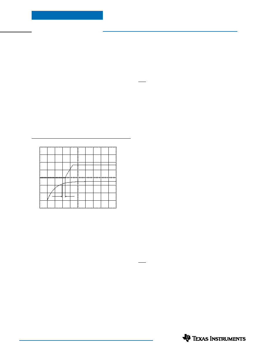
Power up & Soft-Start Timing
Following either the application of a valid input source
voltage, or the removal of a ground signal to the Inhihit*
control pin (with input power applied), the regulator will
initiate a soft-start power up. The soft start slows the
rate at which the output voltage rises, and also introduces a
short time delay, t
d
(approx. 2ms). Figure 1-1 shows the
power-up characteristic of a PT5801 (3.3V) with a 10-A
load.
Vo (2V/Div)
Vin (2V/Div)
HORIZ SCALE: 5ms/Div
t
d
Figure 1-1

For technical support and more information, see inside back cover or visit www.ti.com
Application Notes
Startup of the PT5800 & PT5810 Series ISRs
with Back-Feeding Source (Pre-Bias Capability)
In complex digital systems an external voltage can
sometimes be present at the output of the regulator
during power up. For example, this voltage may be
backfed through a dual-supply logic component such as
an FPGA or ASIC. Another path might be via a clamp
diode (to a lower supply voltage) as part of a power-up
sequencing implementation.
Although the PT5800 (5-V input) and PT5810 (3.3-V
input) series of regulators will sink current under steady-
state operating conditions, they will not do so during
startup
1
as long as certain conditions are maintained
2
.
This feature allows these regulators to start up while an
external voltage is simultaneously applied to the output.
Figure 2-1 is an application schematic that demonstrates
this capability. The waveforms in Figure 2-2 show the
behavior of the circuit as input power is applied. Note
that the plot of the regulator output current (I
o
) is approxi-
mately zero up to the timestamp `A', even though a voltage
is initially backfed to the output via the 3.3-V input supply
and diodes D
1
& D
2
. The regulator sources current
3
when
it begins raising the output above the back-fed voltage to
its nominal regulation value.
Notes
1. Startup includes both the application of a valid input
source voltage, or the removal of a ground signal from
the Inhibit* control (pin 2) with a valid input source
applied. The output of the regulator is effectively off
(tri-state), during the period that the Inhibit* control is
held low.
Vin (1V/Div)
Vo (1V/Div)
Io (5A/Div)
HORIZ SCALE 5ms/Div
A
Figure 2-2; Power-up Waveforms with Back-Feeding Source
Figure 2-1; Schematic Demonstrating Startup into Pre-Bias Capability
PT5812
14≠17
9≠13
5≠7
V
IN
V
OUT
GND
C
out
+
C
IN
+
(3.3VDC)
COM
COM
V
IN
V
O
(2.5V)
8
18
Sense(+)
Sense(≠)
D
2
I
o
D
1
2. To ensure that the regulator does not sink current, the
input voltage must always be greater or equal to the
output voltage throughout the power-up and power-down
sequence.
3. If an external source backfeeding the regulator's output
is greater than the nominal regulation voltage, the output
will begin sinking current at the end of its soft-start
power-up sequence. If this current exceeds the rated
output, the module could be overstressed.
PT5800 & PT5810 Series
Application Notes
For technical support and more information, see inside back cover or visit www.ti.com
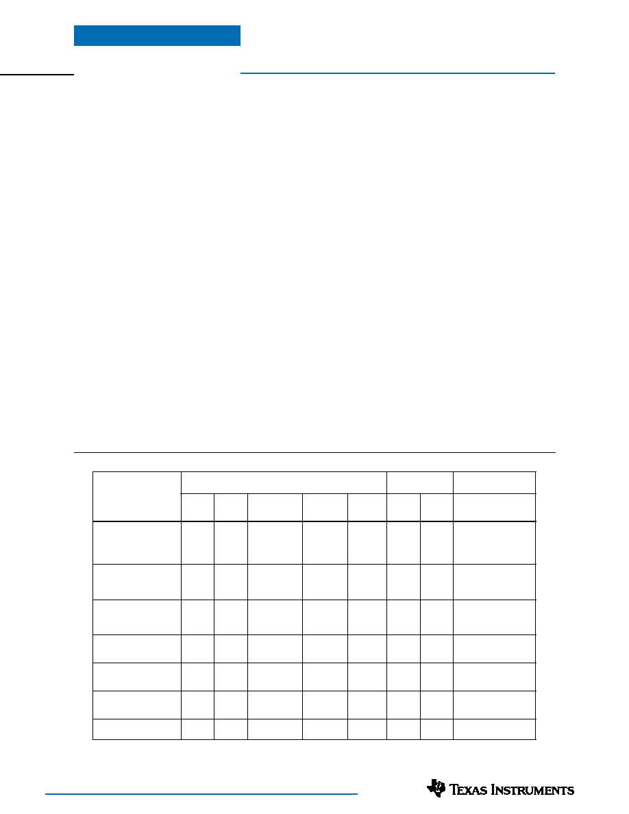
Table 3-1; Input/Output Capacitors
Capacitor Recommendations for the PT5800 &
PT5810 Step-Down Regulator Series
Input Capacitor:
The recommended input capacitance is determined by a
700-mA ripple current rating and the following minimum
capacitance requirements.
∑ PT5800 =
820µF minimum capacitance
∑ PT5810 = 1000µF minimum capacitance
Ripple current and <100m
equivalent series resistance
(ESR) values are the major considerations, along with
temperature, when designing with different types of
capacitors. Tantalum capacitors have a recommended
minimum voltage rating of twice the maximum DC
voltage + AC ripple. This is necessary to ensure reliabil-
ity for input voltage bus applications
Output Capacitors
The ESR of the capacitors is less than 100m
. Electrolytic
capacitors have marginal ripple performance at frequen-
cies greater than 400kHz, but excellent low frequency
transient response. Above the ripple frequency ceramic
capacitors are necessary. Ceramic capacitors improve the
transient response and reduce any high frequency noise
components apparent during high current excursions.
Preferred low-ESR electrolytic capacitor part numbers
are identified in Table 3-1.
PT5800/5810 Series
Tantalum Capacitors (Optional Output Capacitors)
Tantalum type capacitors can be used for the output but
only the AVX TPS series, Sprague 593D/594/595 series,
or Kemet T495/T510 series. These capacitors are rec-
ommended over many other tantalum types due to their
higher rated surge, power dissipation, and ripple current
capability. As a caution the TAJ series by AVX is not
recommended. This series has considerably higher ESR,
reduced power dissipation, and lower ripple current
capability. The TAJ series is less reliable than the AVX
TPS series when determining power dissipation capa-
bility. Tantalum or OsconÆ types are recommended for
applications where ambient temperatures fall below 0∞C.
Capacitor Table
Table 2-1 identifies the characteristics of capacitors from a
number of vendors with acceptable ESR and ripple current
(rms) ratings. The number of capacitors required at both
the input and output buses is identified for each capacitor
type.
This is not an extensive capacitor list. Capacitors from other
vendors are available with comparable specifications. Those listed
are for guidance. The RMS ripple current rating and ESR
(Equivalent Series Resistance at 100kHz) are critical parameters
necessary to insure both optimum regulator performance and
long capacitor life.
s
e
i
r
e
S
/
r
o
d
n
e
V
r
o
t
i
c
a
p
a
C
s
c
i
t
s
i
r
e
t
c
a
r
a
h
C
r
o
t
i
c
a
p
a
C
y
t
i
t
n
a
u
Q
g
n
i
k
r
o
W
e
g
a
t
l
o
V
)
F
µ
(
e
u
l
a
V
t
n
e
l
a
v
i
u
q
E
)
R
S
E
(
e
c
n
a
t
s
i
s
e
R
s
e
i
r
e
S
t
n
e
r
r
u
C
e
l
p
p
i
R
x
a
m
)
s
m
r
(
I
C
∞
5
0
1
@
l
a
c
i
s
y
h
P
)
m
m
(
e
z
i
S
s
u
B
t
u
p
n
I
s
u
B
t
u
p
t
u
O
r
e
b
m
u
N
t
r
a
P
r
o
d
n
e
V
c
i
n
o
s
a
n
a
P
)
l
a
i
d
a
R
(
C
F
)
T
M
S
(
K
F
V
0
1
V
0
1
V
0
1
V
5
3
0
0
0
1
0
6
5
0
0
0
1
0
7
4
8
6
0
.
0
0
9
0
.
0
0
8
0
0
0
6
0
.
0
A
m
0
5
0
1
A
m
5
5
7
A
m
0
5
8
A
m
0
0
1
1
0
1
◊
6
1
0
1
◊
5
.
2
1
0
1
◊
2
.
0
1
5
.
2
1
◊
5
.
3
1
1
2
1
2
1
1
1
1
2
0
1
C
1
C
F
U
E
E
1
6
5
A
1
C
F
U
E
E
P
2
0
1
A
1
K
F
V
E
E
Q
1
7
4
V
1
K
F
V
E
E
n
o
c
-
i
m
e
h
C
d
e
t
i
n
U
s
e
i
r
e
S
V
X
L
/
Z
X
L
s
e
i
r
e
S
X
F
V
6
1
V
0
1
V
0
1
0
7
4
0
0
0
1
0
8
6
0
9
0
.
0
8
6
0
.
0
5
1
0
.
0
A
m
0
6
7
A
m
0
5
0
1
A
m
5
3
7
4
0
1
◊
5
.
2
1
0
1
◊
6
1
0
1
◊
5
.
0
1
2
1
2
1
1
1
L
L
2
1
X
0
1
M
1
7
4
B
V
6
1
Z
X
L
L
L
6
1
X
0
1
M
2
0
1
B
V
0
1
Z
X
L
M
0
8
6
X
F
0
1
n
o
c
i
h
c
i
N
s
e
i
r
e
S
M
P
/
L
P
)
T
M
S
(
s
e
i
r
e
S
X
N
V
0
1
V
6
1
V
0
1
0
0
0
1
0
6
5
0
3
3
5
6
0
.
0
0
8
0
.
0
4
2
0
.
0
A
m
0
4
0
1
A
m
0
2
9
A
m
0
7
7
3
5
.
2
1
◊
5
1
5
.
2
1
◊
5
1
0
1
◊
8
1
2
3
1
1
1
6
H
H
M
2
0
1
A
1
M
P
U
6
H
H
M
1
6
5
C
1
M
P
U
S
G
1
R
C
M
0
3
3
A
1
X
N
P
:
n
o
c
-
s
O
o
y
n
a
S
P
S
)
T
M
S
(
P
V
S
V
0
1
V
0
1
0
7
4
0
6
5
5
1
0
.
0
3
1
0
.
0
A
m
0
0
5
4
>
A
m
0
0
2
5
>
0
1
◊
5
.
0
1
1
1
◊
7
.
2
1
2
2
1
1
0
7
4
P
S
0
1
M
M
0
6
5
P
V
S
0
1
)
T
M
S
(
S
P
T
m
u
l
a
t
n
a
T
X
V
A
V
0
1
V
0
1
0
7
4
0
7
4
5
4
0
.
0
0
6
0
.
0
A
m
3
2
7
1
A
m
6
2
8
1
L
3
.
7
◊
W
7
.
5
◊
H
1
.
4
2
2
1
1
4
0
0
R
0
1
0
M
7
7
4
E
S
P
T
5
0
6
0
0
R
0
1
0
M
7
7
4
V
S
P
T
m
u
l
a
t
n
a
T
r
e
m
y
l
o
P
t
e
m
e
K
(
s
e
i
r
e
S
0
3
5
T
/
0
2
5
T
T
M
S
)
V
0
1
V
0
1
0
3
3
0
3
3
0
4
0
.
0
5
1
0
.
0
A
m
0
0
8
1
A
m
0
0
8
3
>
3
.
7
◊
3
.
4
◊
4
3
3
1
1
S
A
0
1
0
M
7
3
3
X
0
2
5
T
S
A
0
1
0
M
7
3
3
X
0
3
5
T
m
u
l
a
t
n
a
T
e
u
g
a
r
p
S
(
s
e
i
r
e
S
D
4
9
5
T
M
S
)
V
0
1
0
8
6
0
9
0
.
0
A
m
0
6
6
1
2
.
7
◊
6
◊
1
.
4
2
1
T
2
R
0
1
0
0
X
7
8
6
D
5
9
5
For technical support and more information, see inside back cover or visit www.ti.com
Application Notes
Using the Inhibit Control of the PT5800 & PT5810
Series of Step-Down ISRs
For applications requiring output voltage On/Off control,
the PT5800 & PT5810 series of ISRs incorporate an
inhibit function. This function can be used wherever there
is a requirement for the output voltage from the ISR to be
turned off. The On/Off function is provided by the Inhibit*
control (pin 2).
The ISR functions normally with pin 2 open-circuit,
providing a regulated output whenever a valid source
voltage is applied between V
in
(pins 5≠7) and GND (pins
9≠13). When a low-level
ground signal is applied to
pin 2, the regulator output is turned off
2
.
Figure 4-1 shows the typical application of the Inhibit*
function. Note the discrete transistor (Q
1
). The Inhibit*
control has its own internal pull-up to +V
in
potential. An
open-collector or open-drain device is recommended to
control this input
1
. The voltage thresholds are given in
Table 4-1.
Table 4-1; Inhibit Control Requirements
Parameter
Min
Typ
Max
Enable (VIH)
Vin ≠ 0.5V
--
Open
Disable (VIL)
≠0.2V
--
+0.8V
I IL
--
≠0.5 mA
--
Notes:
1. Use an open-collector device with a breakdown voltage
of at least 10V (preferably a discrete transistor) for the
Inhibit* input. A pull-up resistor is not necessary. To
disable the output voltage the control pin should be
pulled low to less than +0.8VDC.
2. When a ground signal is applied to the Inhibit* control
(pin 2) the module output is turned off (tri-state). The
output voltage decays to zero as the load impedance
discharges the output capacitors.
Figure 4-1
Turn-On Time:
In the circuit of Figure 4-1, turning Q
1
on
applies a low-voltage to the Inhibit* control (pin 2) and
disables the output of the regulator
2
. If Q
1
is then turned
off, the ISR executes a soft-start power up. Power up
consists of a short delay (approx. 2msec), followed by a
period in which the output voltage rises to its full regu-
lation voltage. The module produces a regulated output
voltage within 10msec. Figure 4-2 shows the typical rise
in both the output voltage and input current for a PT5812
(2.5V), following the turn-off of Q
1
. The turn off of Q
1
corresponds to the rise in the waveform, Q
1
V
ds
. The
waveforms were measured with a 3.3VDC input voltage,
and 10-A load.
Figure 4-2
Vo (1V/Div)
Iin (5A/Div)
Q1 Vds (2V/Div)
HORIZ SCALE: 2ms/Div
PT5800 & PT5810 Series
PT5812
V
IN
9≠13
4
1
18
14≠17
5, 6, 7
8
2
C
IN
1,000µF
+
C
OUT
330µF
+
1 =Inhibit
GND
GND
V
OUT
3
Output Sense (+)
Output Sense (≠)
Q
1
BSS138
Application Notes
For technical support and more information, see inside back cover or visit www.ti.com
PT5800 & PT5810 Series
Adjusting the Output Voltage of the PT5800 &
PT5810 Step-Down Series of Regulators
Using Margin Up/ Margin Down
The Margin Up* (pin 4) and Margin Dn* (pin 3) control
inputs allow the output voltage to be easily adjusted by
up to ±5% of the nominal set-point voltage. To activate,
simply connect the appropriate control input to the Sense(≠)
(pin 8), or the local starpoint ground. Either a logic level
MOSFET or a p-channel JFET is recommended for this
purpose. For further information see the related applica-
tion note on this feature.
Using the `V
o
Adjust' Control
For a more permanent and precise adjustment, use the
Vo Adjust control (pin 1). The V
o
Adjust control allows
adjustment in any increment by up to ±10% of the set-
point. The adjustment method requires the addition of a
single external resistor. Table 5-1 gives the allowable
adjustment range for each model of the series as V
a
(min)
and V
a
(max). The value of the external resistor can either
be calculated using the formulas given below, or simply
selected from the range of values provided in Table 5-2.
Refer to Figure 5-1 for the placement of the required
resistor. Use the resistor R
1
to adjust up, and the resistor
(R
2
)
to adjust down.
Adjust Up: An increase in the output voltage is obtained
by adding a resistor R
1
, between V
o
Adjust (pin 1) and
Sense(≠) (pin 8). See Figure 5-1.
Adjust Down: Add a resistor
(R
2
)
, between V
o
Adjust (pin 1)
and Sense(+) (pin 18). See Figure 5-1.
Figure 5-1; V
o
Adjust Resistor Placement
V
o
Adjust Resistor Calculations
The values of R
1
[adjust up] and
(R
2
)
[adjust down] can
also be calculated using the following formulas. Again, use
Figure 5-1for the placement of the required resistor;
either R
1
or
(R
2
)
as appropriate.
R
1
=
V
r
∑ R
o
≠ 24.9
k
V
a
≠ V
o
(R
2
)
=
R
o
(V
a
≠ V
r
)
≠ 24.9
k
V
o
≠ V
a
Where: V
o
= Original output voltage
V
a
= Adjusted output voltage
V
r
= The reference voltage in Table 5-1
R
o
= The resistance constant in Table 5-1
Table 5-1
ISR OUTPUT VOLTAGE ADJUSTMENT RANGE AND FORMULA PARAMETERS
Series Pt. No.
5.0V Bus
PT5801
PT5802
PT5803
PT5804
PT5805
PT5806
3.3V Bus
N/A
PT5812
4
PT5813
PT5814
PT5815
PT5816
Vo (nom)
3.3V
2.5V
1.8V
1.5V
1.2V
1.0V
Va (min)
2.6V
2.0V
1.52V
1.31V
1.1V
0.94V
Va (max)
3.63V
2.8V #
2.1V
1.82V
1.52V
1.32V
Vr
0.8V
0.8V
0.8V
0.8V
0.8V
0.8V
Ro (k
)
10.2
10.7
10.2
9.76
10.0
10.2
# The PT5812 should not be adjusted higher than its nominal output voltage of 2.5V. See note 4.
Notes:
1. Use a 1% (or better) tolerance resistor in either the R
1
or
(R
2
)
location. Place the resistor as close to the ISR as
possible.
2. Never connect capacitors from V
o
Adjust to either GND or
V
out
. Any capacitance added to the V
o
Adjust pin will affect
the stability of the ISR.
3. If the remote sense feature is not being used, the adjust
resistor
(R
2
)
can be connected to V
out
, (pins 14-17) instead
of Sense (+).
PT5800/5810
9≠13
1
18
14≠17
8
C
OUT
330µF
+
GND
V
OUT
Sense (+) [Note 3]
Sense (≠)
(R
2
)
Adj Down
V
O
Adj
GND
Sense(+)
Sense(≠)
V
OUT
R
1
Adjust Up
4. The PT5812 may not be adjusted higher than the
nominal output voltage of 2.5V. There is insufficient
input voltage between V
in
and V
out
to accommodate
an increase in the output voltage.
For technical support and more information, see inside back cover or visit www.ti.com
Application Notes
continued
V
a
(req.d)
2.100
2.3k
2.050
7.7k
2.000
15.9k
1.950
29.5k
1.900
56.7k
1.850
138.0k
1.800
1.1k
1.750
(169.0)k
6.3k
1.700
(66.9)k
14.1k
1.650
(32.9)k
27.2k
1.600
(15.9)k
53.2k
1.550
(5.7)k
131.0k
1.500
1.8k
1.475
(239.0)k
4.2k
1.450
(102.0)k
7.1k
1.425
(56.4)k
10.7k
1.400
(33.7)k
15.1k
1.375
(20.0)k
20.8k
1.350
(10.9)k
28.4k
1.325
(4.4)k
39.1k
1.300
55.1k
2.3k
1.275
81.8k
4.8k
1.250
135.0k
7.7k
1.225
295.0k
11.4k
1.200
15.9k
1.175
(125.0)k
21.7k
1.150
(45.1)k
29.5k
1.125
(18.4)k
40.4k
1.100
(5.1)k
56.7k
1.075
83.9k
1.050
138.0k
1.025
302.0K
1.000
0.975
(46.5)k
0.950
(5.7)k
PT5800 & PT5810 Series
Table 5-2
ISR ADJUSTMENT RESISTOR VALUES
Series Pt. No.
5.0V Bus
PT5801
PT5802
PT5803
PT5804
PT5805
PT5806
3.3V Bus
N/A
PT5812
PT5813
PT5814
PT5815
PT5816
V
o
(nom)
3.3V
2.5V
1.8V
1.5V
1.2V
1.0V
V
a
(req.d)
3.60
2.3k
3.55
7.7k
3.50
15.9k
3.45
29.5k
3.40
56.7k
3.35
138.0k
3.30
3.25
(475.0)k
3.20
(220.0)k
3.15
(135.0)k
3.10
(92.4)k
3.05
(66.9)k
3.00
(49.9)k
2.95
(37.5)k
2.90
(28.6)k
2.85
(21.6)k
2.80
(15.9)k
3.6K
2.75
(11.3)k
9.3K
2.70
(7.4)k
17.9K
2.65
(4.1)k
32.2K
2.60
(1.3)k
60.7K
2.550
[Note 4
]
146.0K
2.500
2.450
(321.0)k
2.400
(146.0)k
2.350
(85.7)k
2.300
(55.3)k
2.250
(37.2)k
2.200
(25.0)k
2.150
(16.4)k
2.100
(9.9)k
2.050
(4.8)k
2.000
(0.8)k
R
1
= Black
R
2
=
(Blue)
Application Notes
For technical support and more information, see inside back cover or visit www.ti.com
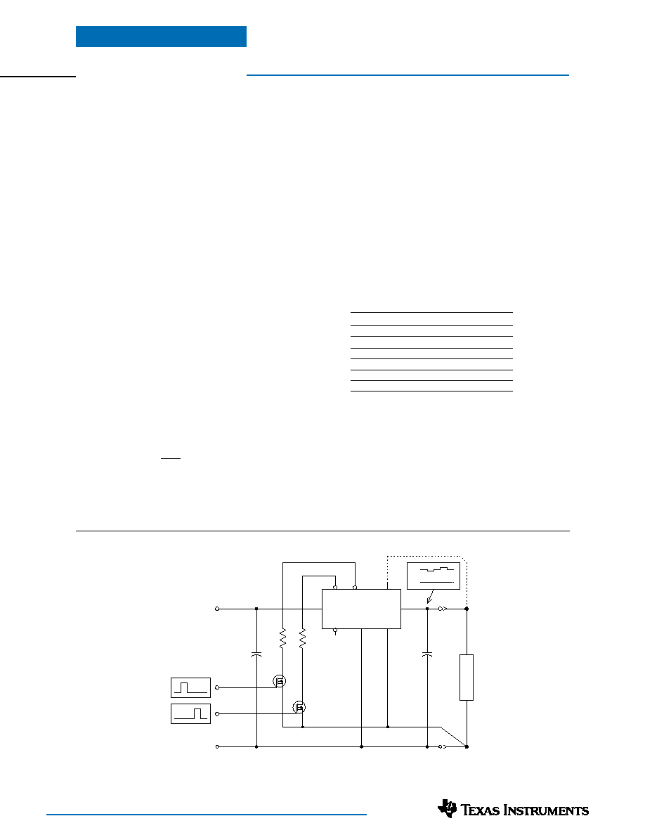
Using the Margin Up/Down Controls on the
PT5800 & PT5810 Regulator Series
The PT5800 & PT5810 series of integrated switching
regulator modules incorporate Margin Up* (pin 4) and
Margin Dn* (pin 3) control inputs. These controls allow the
output voltage set point to be momentarily adjusted
1
,
either up or down, by a nominal 5%. This provides a
convenient method for dynamically testing the load
circuit's power supply voltage over its operating margin
or range. Note that the ±5% change is also applied to any
adjustment of the output voltage, if made, using the V
o
Adjust (pin 1).
The 5% adjustment is made by driving the appropriate
margin control input directly to the ground reference at
Sense(-) (pin 8)
2
. An low-leakage open-drain device, such as
a MOSFET or a p-channel JFET is recommended for this
purpose. Adjustments of less than 5% can also be accom-
modated by adding series resistors to the control inputs
(See Figure 6-1). The value of the resistor can be selected
from Table 6-1, or calculated using the following formula.
Resistor Value Calculation
To reduce the margin adjustment to something less than
5%, series padding resistors are required (See R
D
and
R
U
in Figure 6-1). For the same amount of adjustment,
the resistor value calculated for R
U
and R
D
will be the
same. The formulas is as follows.
R
U
/R
D
=
499
≠ 99.8
k
%
Where
% = The desired amount of margin adjust in
percent.
Notes:
1. The Margin Up* and Margin Dn* controls were not
intended to be activated simultaneously. If they are
their affects on the output voltage may not completely
cancel, resulting in a slight shift in the output voltage
set point.
2. When possible use the Sense(-) (pin 8) as the ground
reference. This will produce a more accurate adjustment
of the output voltage at the load circuit terminals. GND
(pins 9-13) can be used if the Sense(-) pin is connected
to GND near the regulator.
C
out
+
C
in
+5V
GND
MargDn
L
O
A
D
Q
2
Sense(≠)
+V
OUT
GND
PT5800
18
14≠17
8
2
9≠13
5, 6, 7
V
OUT
V
IN
GND
SNS(+)
SNS(≠)
INHIBIT*
Q
1
4
3
MARG
DN*
MARG
UP*
+
MargUp
0V
+V
o
R
D
R
U
0V
Figure 6-1; Margin Up/Down Application Schematic
Table 6-1; Margin Up/Down Resistor Values
PADDING RESISTOR VALUES
% Adjust
R
U
/ R
D
5
0.0k
4
24.9k
3
66.5k
2
150.0k
1
397.0k
PT5800 & PT5810 Series

IMPORTANT NOTICE
Texas Instruments Incorporated and its subsidiaries (TI) reserve the right to make corrections, modifications,
enhancements, improvements, and other changes to its products and services at any time and to discontinue
any product or service without notice. Customers should obtain the latest relevant information before placing
orders and should verify that such information is current and complete. All products are sold subject to TI's terms
and conditions of sale supplied at the time of order acknowledgment.
TI warrants performance of its hardware products to the specifications applicable at the time of sale in
accordance with TI's standard warranty. Testing and other quality control techniques are used to the extent TI
deems necessary to support this warranty. Except where mandated by government requirements, testing of all
parameters of each product is not necessarily performed.
TI assumes no liability for applications assistance or customer product design. Customers are responsible for
their products and applications using TI components. To minimize the risks associated with customer products
and applications, customers should provide adequate design and operating safeguards.
TI does not warrant or represent that any license, either express or implied, is granted under any TI patent right,
copyright, mask work right, or other TI intellectual property right relating to any combination, machine, or process
in which TI products or services are used. Information published by TI regarding third≠party products or services
does not constitute a license from TI to use such products or services or a warranty or endorsement thereof.
Use of such information may require a license from a third party under the patents or other intellectual property
of the third party, or a license from TI under the patents or other intellectual property of TI.
Reproduction of information in TI data books or data sheets is permissible only if reproduction is without
alteration and is accompanied by all associated warranties, conditions, limitations, and notices. Reproduction
of this information with alteration is an unfair and deceptive business practice. TI is not responsible or liable for
such altered documentation.
Resale of TI products or services with statements different from or beyond the parameters stated by TI for that
product or service voids all express and any implied warranties for the associated TI product or service and
is an unfair and deceptive business practice. TI is not responsible or liable for any such statements.
Mailing Address:
Texas Instruments
Post Office Box 655303
Dallas, Texas 75265
Copyright
2003, Texas Instruments Incorporated