For assistance or to order, call
(800) 531-5782
Power Trends, Inc.
27715 Diehl Road, Warrenville, IL 60555
(800) 531-5782
Fax: (630) 393-6902 http://www.ti.com/powertrends
4
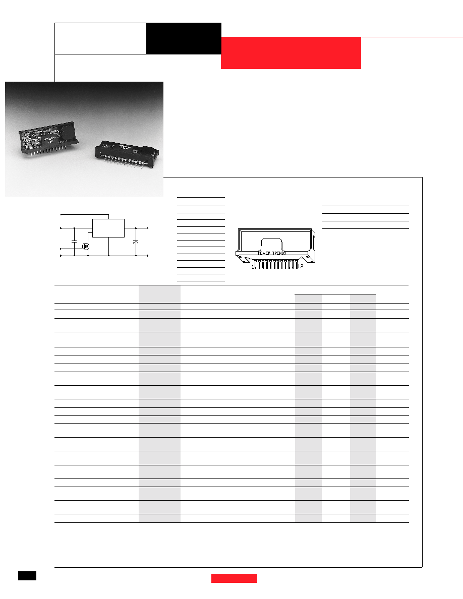
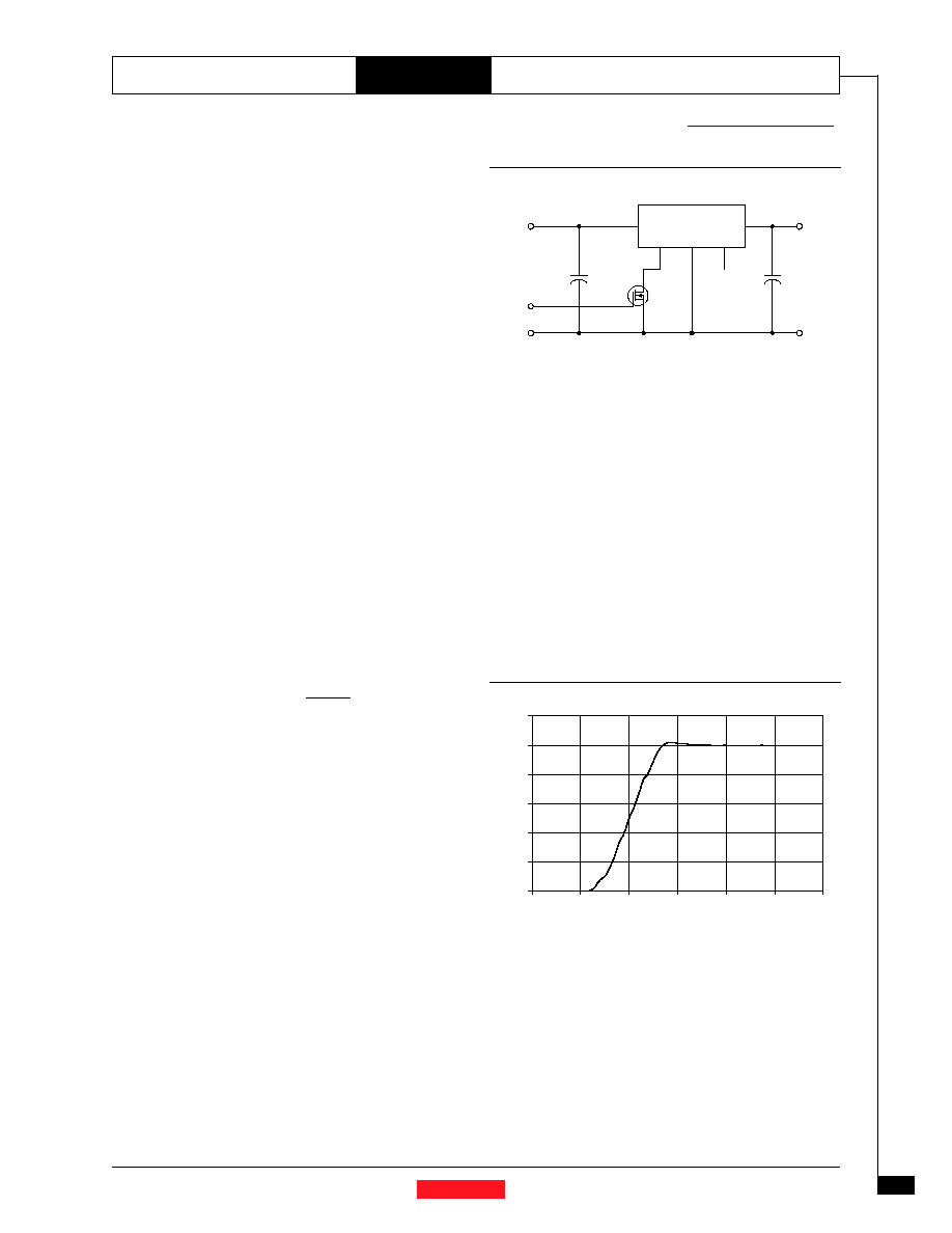
Standard Application
Ordering Information
PT6121! = +5 Volts
PT6122! = +3.3 Volts
PT Series Suffix
(PT1234
X
)
Case/Pin
Configuration
Vertical Through-Hole
N
Horizontal Through-Hole
A
Horizontal Surface Mount
C
Pin-Out Information
P T 6 1 2 0
S e r i e s
�
Low Voltage Input (7V)
�
89% Efficiency
�
Adjustable Output Voltage
�
Internal Short Circuit Protection
�
Over-Temperature Protection
�
On/Off Control (Ground Off)
The PT6120 series is a low volt-
age input (typically 7V) version of
Power Trends' high-performance
1A, 12 pin SIP Integrated Switching
Regulators (ISRs). These ISRs are de-
signed with premium low threshold FETs
for those applications requiring very low
input/output voltage differentials such as
battery powered equipment. This high-
performance ISR family offers a unique
combination of features combining 89%
typical efficiency with open-collector on/
off control and adjustable output voltage.
Quiescent current in the shutdown mode
is less than 100�A.
1 AMP ADJUSTABLE LOW VOLTAGE INPUT
INTEGRATED SWITCHING REGULATOR
C
1
= Optional 1�F ceramic
Q
1
=NFET
C
2
= Required 100�F electrolytic
Pin
Function
1
Inhibit
(30V max)
2
V
in
3
V
in
4
V
in
5
GND
6
GND
7
GND
8
GND
9
V
out
10
V
out
11
V
out
12
V
out
Adj
PT6120
2,3,4
5,6,7,8
9,10,11
12
V
IN
GND
GND
V
OUT
C2
+
1
V
O
ADJ
INH
Q1
C1
Specifications
Characteristics
PT6120 SERIES
(T
a
=25
�
C unless noted)
Symbols
Conditions
Min
Typ
Max
Units
Output Current
I
o
Over V
in
range
0.1*
--
1.0
A
Short Circuit Current
I
sc
V
in
= V
in
min
--
3.5
--
Apk
Input Voltage Range
V
in
0.1
I
o
1.0 A
V
o
= 3.3V
7
--
26
V
(Note: inhibit function cannot be used with Vin above 30V)
V
o
= 5V
7
--
30/38**
V
Output Voltage Tolerance
V
o
Over V
in
Range, I
o
= 1.0 A
--
�1.0
�2.0
%V
o
T
a
= 0�C to +60�C
Line Regulation
Reg
line
Over V
in
range
--
�0.25
�0.5
%V
o
Load Regulation
Reg
load
0.1
I
o
1.0 A
--
�0.25
�0.5
%V
o
V
o
Ripple/Noise
V
n
V
in
=V
in
min, I
o
=1.0 A
--
�2
--
%V
o
Transient Response
t
tr
50% load change
--
100
200
�Sec
with C
o
= 100�F
V
os
V
o
over/undershoot
--
5.0
--
%V
o
Efficiency
V
in
=9V, I
o
=0.5A, V
o
=3.3V
--
84
--
%
V
in
=9V, I
o
=0.5A, V
o
=5V
--
89
--
%
Switching Frequency
o
Over V
in
and I
o
ranges
400
500
600
kHz
Shutdown Current
I
sc
V
in
= 15V
--
100
--
�A
Quiescent Current
I
nl
I
o
= 0A, V
in
=10V
--
10
--
mA
Output Voltage
V
o
Below V
o
See Application Notes.
Adjustment Range
Above V
o
Absolute Maximum
T
a
-40
--
+85
�
C
Operating Temperature Range
Recommended Operating
T
a
Free Air Convection, V
o
= 3.3V
-40
--
+85***
�
C
Temperature Range
(40-60LFM)
V
o
= 5V
-40
--
+85***
Thermal Resistance
ja
Free Air Convection
V
o
= 3.3V
--
50
--
�
C/W
(40-60LFM)
V
o
= 5V
--
40
--
Storage Temperature
T
s
-40
--
+125
�
C
Mechanical Shock
Per Mil-STD-883D, Method 2002.3
--
500
--
G's
1 msec, Half Sine, mounted to a fixture
Mechanical Vibration
Per Mil-STD-883D, Method 2007.2
--
10
--
G's
20-2000 Hz, Soldered in a PC board
Weight
--
5.0
--
grams
* ISR will operate down to no load with reduced specifications.
** Input voltage cannot exceed 30V when the inhibit function is used. ***See Thermal Derating chart.
Note: The PT6120 Series requires a 100�F electrolytic or tantalum output capacitor for proper operation in all applications.
Pkg Style 200
PT6120
SLTS081
(Revised 6/4/98)
For assistance or to order, call
(800) 531-5782
Power Trends, Inc.
27715 Diehl Road, Warrenville, IL 60555
(800) 531-5782
Fax: (630) 393-6902 http://www.ti.com/powertrends
5
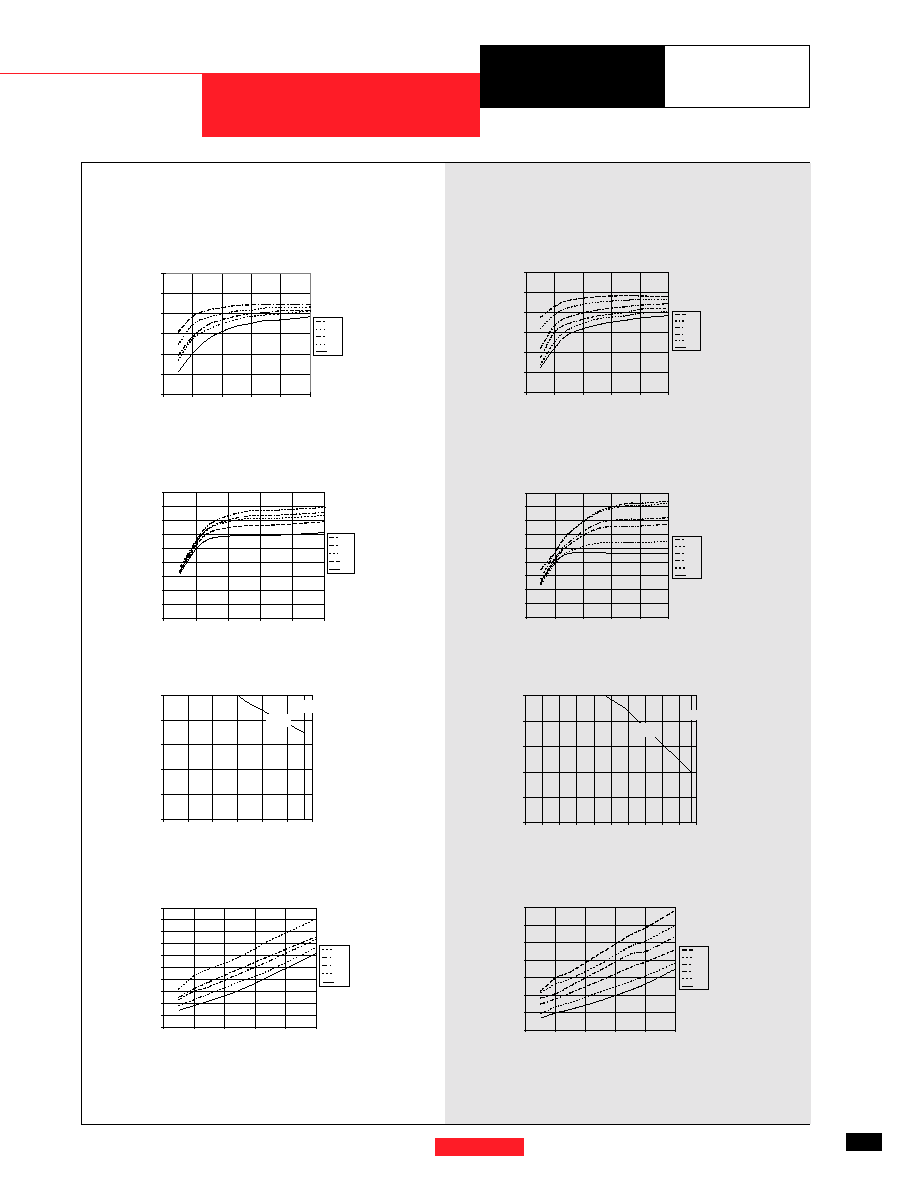
C H A R A C T E R I S T I C D A T A
0
0.2
0.4
0.6
0.8
1
9
12
15
18
21
24
27
(n
0
0.2
0.4
0.6
0.8
1
9
12
15
18
21
24
27
30
33
36
39
PT6122, 3.3 VDC
(See Note 1)
PT6121, 5.0 VDC
(See Note 1)
Note 1:
All data listed in the above graphs, except for derating data, has been developed from actual products tested at 25�C. This data is considered typical data for the ISR.
Note 2:
Thermal derating graphs are developed in free air convection cooling of 40-60 LFM. (See Thermal Application Notes.)
Efficiency - %
Ripple-(mV)
Iout-(Amps)
PD-(W
atts)
Efficiency - %
Ripple-(mV)
Iout-(Amps)
PD-(W
atts)
Iout-(Amps)
Iout-(Amps)
Iout-(Amps)
Iout-(Amps)
Iout-(Amps)
Iout-(Amps)
Vin-(Volts)
Vin-(Volts)
40
50
60
70
80
90
100
0
0.2
0.4
0.6
0.8
1
9.0V
12.0V
15.0V
18.0V
26.0V
Vin
85�C
70�C
0
20
40
60
80
100
120
140
160
180
0
0.2
0.4
0.6
0.8
1
38.0V
30.0V
24.0V
18.0V
12.0V
9.0V
Vin
40
50
60
70
80
90
100
0
0.2
0.4
0.6
0.8
1
9.0V
12.0V
18.0V
24.0V
30.0V
38.0V
Vin
0
0.2
0.4
0.6
0.8
1
1.2
1.4
0
0.2
0.4
0.6
0.8
1
38.0V
30.0V
24.0V
18.0V
12.0V
9.0V
Vin
0
10
20
30
40
50
60
70
80
90
0
0.2
0.4
0.6
0.8
1
26.0V
18.0V
15.0V
12.0V
9.0V
Vin
0
0.1
0.2
0.3
0.4
0.5
0.6
0.7
0.8
0.9
1
0
0.2
0.4
0.6
0.8
1
26.0V
18.0V
15.0V
12.0V
9.0V
Vin
P T 6 1 2 0
S e r i e s
70�C
85�C
Efficiency vs Output Current
Efficiency vs Output Current
Ripple vs Output Current
Ripple vs Output Current
Thermal Derating (T
a
)
(See Note 2)
Thermal Derating (T
a
)
(See Note 2)
Power Dissipation vs Output Current
Power Dissipation vs Output Current
For assistance or to order, call
(800) 531-5782
3
Power Trends, Inc.
27715 Diehl Road, Warrenville, IL 60555
(800) 531-5782
Fax: (630) 393-6902 http://www.powertrends.com
A p p l i c a t i o n
N o t e s
PT6100/6120/6210/6220/6300/6320 Series
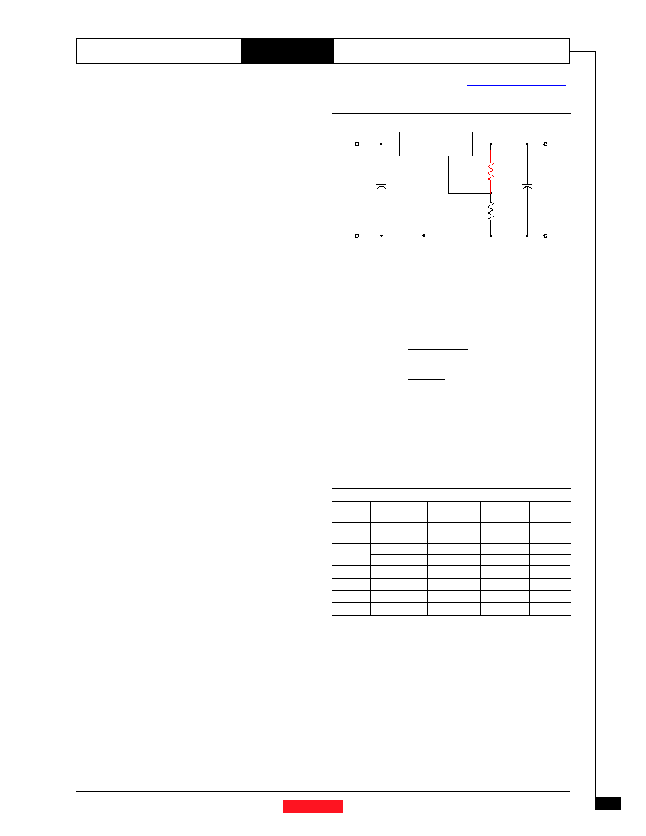
Adjusting the Output Voltage of Power Trends'
Wide Input Range Bus ISRs
The output voltage of the Power Trends' Wide Input Range
Series ISRs may be adjusted higher or lower than the factory
trimmed pre-set voltage with the addition of a single external
resistor. Table 1 accordingly gives the allowable adjustment
range for each model for either series as V
a
(min) and V
a
(max).
Adjust Up:
An increase in the output voltage is obtained by
adding a resistor R2, between pin 12 (V
o
adjust) and pins 5-8
(GND).
Adjust Down:
Add a resistor
(R1)
, between pin 12 (V
o
adjust)
and pins 9-11(V
out
).
Refer to Figure 1 and Table 2 for both the placement and value
of the required resistor; either
(R1)
or R2 as appropriate.
Notes:
1. Use only a single 1% resistor in either the
(R1)
or R2 loca-
tion. Place the resistor as close to the ISR as possible.
2. Never connect capacitors from V
o
adjust to either GND or
V
out
. Any capacitance added to the V
o
adjust pin will affect
the stability of the ISR.
4. Adjustments to the output voltage may place additional
limits on the maximum and minimum input voltage for the
part. The revised maximum and minimum input voltage
limits must comply with the following requirements. Note
that the minimum input voltage limits are also model depen-
dant.
V
in
(max) = (8 x V
a
)V or
*
30/38V,
whichever is less.
*
Limit is 30V when inhibit function is active.
PT6x
0
x/PT6x
1
x series:
V
in
(min) = (V
a
+ 4)V or 9V,
whichever is greater.
PT6x
2
x series:
V
o
<10V;
V
in
(min) = (V
a
+ 2.0)V or 7.0V,
whichever is greater.
V
o
10V;
V
in
(min) = (V
a
+ 2.5)V
Figure 1
The values of
(R1)
[adjust down], and R2 [adjust up], can
also be calculated using the following formulae.
R
o
(V
a
� 1.25)
(R1)
=
V
o
� V
a
k
1.25 R
o
k
R2
=
V
a
� V
o
Where: V
o
= Original output voltage
V
a
= Adjusted output voltage
R
o
= The resistance value fromTable 1
Table 1
ISR ADJUSTMENT RANGE AND FORMULA PARAMETERS
1Adc Rated
PT6102
PT6101
PT6103
PT6122
PT6121
2Adc Rated
PT6213
PT6212
PT6214
PT6223
PT6222
3Adc Rated
PT6303
PT6302
PT6304
PT6323
PT6322
Vo (nom)
3.3
5.0
5.0
12.0
Va (min)
1.89
1.88
2.18
2.43
Va (max)
6.07
11.25
8.5
22.12
Ro (k
)
66.5
150.0
90.9
243.0
R 2
Adjust Up
C 1
1
�
F Ceramic
(Optional)
C 2
100
�
F
(Req'd)
Vo
C O M
C O M
Vin
+
(R1)
Adj Down
PT6100/6200/6300
9 , 1 0 , 1 1
1 2
5,6,7,8
2,3,4
Vin
V o
G N D
Vo(adj)
More Application Notes
For assistance or to order, call
(800) 531-5782
4
A p p l i c a t i o n
Power Trends, Inc.
27715 Diehl Road, Warrenville, IL 60555
(800) 531-5782
Fax: (630) 393-6902 http://www.powertrends.com
N o t e s
PT6100/6120/6210/6220/6300/6320 Series
ISR ADJUSTMENT RESISTOR VALUES (Cont)
1Adc Rated
PT6101
PT6103
PT6121
2Adc Rated
PT6212
PT6214
PT6222
3Adc Rated
PT6302
PT6304
PT6322
V
o
(nom)
5.0
5.0
12.0
V
a
(req.d)
6.2
156.0k
94.7k
(207.0)k
6.4
134.0k
81.2k
(223.0)k
6.6
117.0k
71.0k
(241.0)k
6.8
104.0k
63.1k
(259.0)k
7.0
93.8k
56.8k
(279.0)k
7.2
85.2k
51.6k
(301.0)k
7.4
78.1k
47.3k
(325.0)k
7.6
72.1k
43.7k
(351.0)k
7.8
67.0k
40.6k
(379.0)k
8.0
62.5k
37.9k
(410.0)k
8.2
58.6k
35.5k
(444.0)k
8.4
55.1k
33.4k
(483.0)k
8.6
52.1k
(525.0)k
8.8
49.3k
(573.0)k
9.0
46.9k
(628.0)k
9.5
41.7k
(802.0)k
10.0
37.5k
(1060.0)k
10.5
34.1k
(1500.0)k
11.0
31.3k
11.5
12.0
12.5
608.0k
13.0
304.0k
13.5
203.0k
14.0
152.0k
14.5
122.0k
15.0
101.0k
15.5
86.8k
16.0
75.9k
16.5
67.5k
17.0
60.8k
17.5
55.2k
18.0
50.6k
18.5
46.7k
19.0
43.4k
19.5
40.5k
20.0
38.0k
20.5
35.7k
21.5
33.8k
21.5
32.0k
22.0
30.4k
ISR ADJUSTMENT RESISTOR VALUES
1Adc Rated
PT6102
PT6101
PT6103
PT6122
PT6121
2Adc Rated
PT6213
PT6212
PT6214
PT6223
PT6222
3Adc Rated
PT6303
PT6302
PT6304
PT6323
PT6322
V
o
(nom)
3.3
5.0
5.0
12.0
V
a
(req.d)
1.9
(30.9)k
(31.5)k
2.0
(38.4)k
(37.5)k
2.1
(47.1)k
(44.0)k
2.2
(57.4)k
(50.9)k
(30.8)k
2.3
(69.8)k
(58.3)k
(35.4)k
2.4
(85.0)k
(66.3)k
(40.2)k
2.5
(104.0)k
(75.0)k
(45.5)k
(32.0)k
2.6
(128.0)k
(84.4)k
(51.1)k
(34.9)k
2.7
(161.0)k
(94.6)k
(57.3)k
(37.9)k
2.8
(206.0)k
(106.0)k
(64.0)k
(40.9)k
2.9
(274.0k
(118.0)k
(71.4)k
(44.1)k
3.0
(388.0)k
(131.0)k
(79.5)k
(47.3)k
3.1
(615.0)k
(146.0)k
(88.5)k
(50.5)k
3.2
(1300.0)k
(163.0)k
(98.5)k
(53.8)k
3.3
(181.0)k
(110.0)k
(57.3)k
3.4
831.0k
(202.0)k
(122.0)k
(60.8)k
3.5
416.0k
(225.0)k
(136.0)k
(64.3)k
3.6
227.0k
(252.0)k
(153.0)k
(68.0)k
3.7
208.0k
(283.0)k
(171.0)k
(71.7)k
3.8
166.0k
(319.0)k
(193.0)k
(75.6)k
3.9
139.0k
(361.0)k
(219.0)k
(79.5)k
4.0
119.0k
(413.0)k
(250.0)k
(83.5)k
4.1
104.0k
(475.0)k
(288.0)k
(87.7)k
4.2
92.4k
(533.0)k
(335.0)k
(91.9)k
4.3
83.1k
(654.0)k
(396.0)k
(96.3)k
4.4
75.6k
(788.0)k
(477.0)k
(101.0)k
4.5
69.3k
(975.0)k
(591.0)k
(105.0)k
4.6
63.9k
(1260.0)k
(761.0)k
(110.0)k
4.7
59.4k
(1730.0)k
(1050.0)k
(115.0)k
4.8
55.4k
(1610.0)k
(120.0)k
4.9
52.0k
(125.0)k
5.0
48.9k
(130.0)k
5.1
46.2k
1880.0k
1140.0k
(136.0)k
5.2
43.8k
937.0k
568.0k
(141.0)k
5.3
41.6k
625.0k
379.0k
(147.0)k
5.4
39.6k
469.0k
284.0k
(153.0)k
5.5
37.8k
375.0k
227.0k
(159.0)k
5.6
36.1k
313.0k
189.0k
(165.0)k
5.7
34.6k
268.0k
162.0k
(172.0)k
5.8
33.3k
234.0k
142.0k
(178.0)k
5.9
32.0k
208.0k
126.0k
(185.0)k
6.0
30.8k
188.0k
114.0k
(192.0)k
Table 2
R1 =
(Red)
R2 = Black
For assistance or to order, call
(800) 531-5782
5
Power Trends, Inc.
27715 Diehl Road, Warrenville, IL 60555
(800) 531-5782
Fax: (630) 393-6902 http://www.powertrends.com
A p p l i c a t i o n
N o t e s
PT6100/6120/6210/6220/6300/6320 Series
More Application Notes
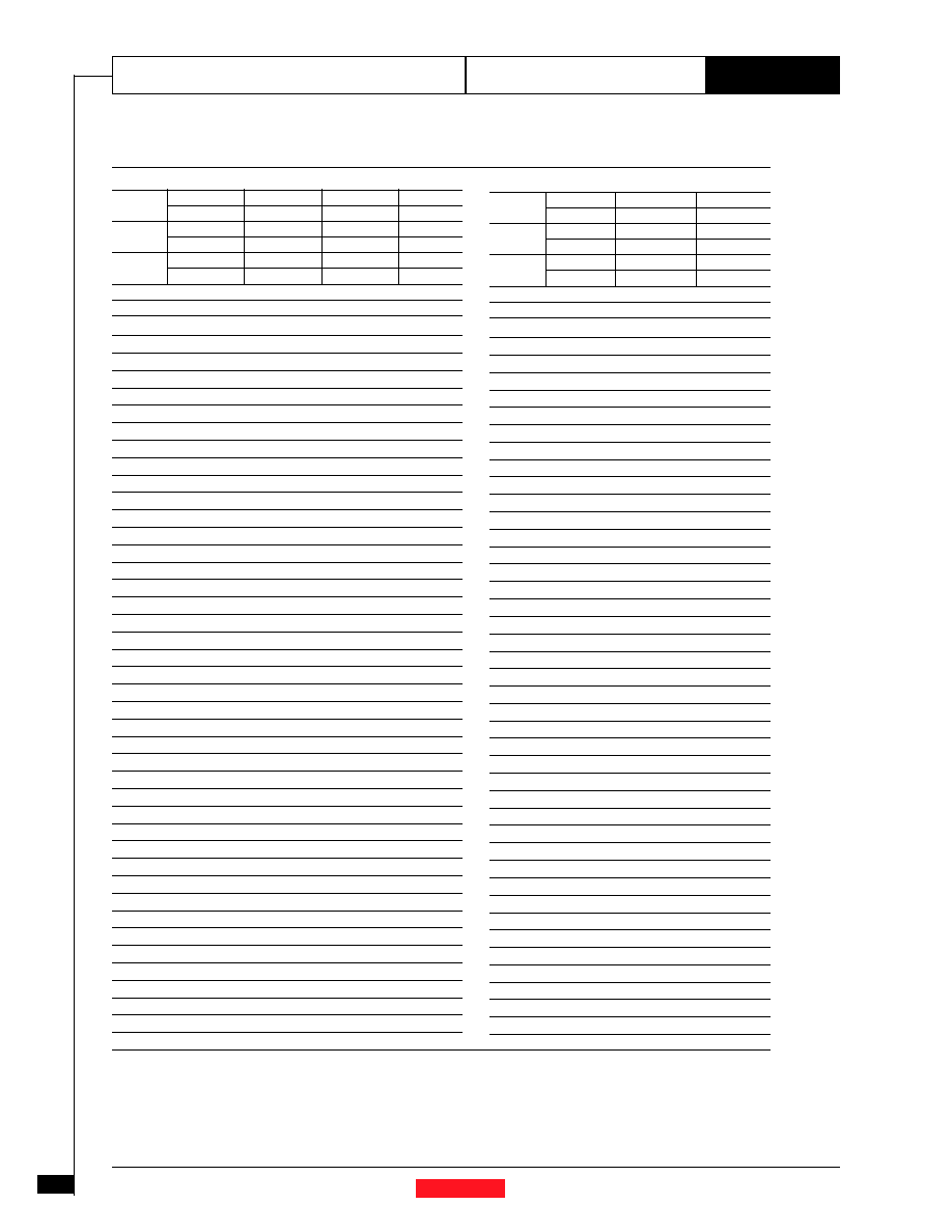
Using the Inhibit Function on Power Trends'
Wide Input Range Bus ISRs
For applications requiring output voltage On/Off control, the
12pin ISR products incorporate an inhibit function. The func-
tion has uses in areas such as battery conservation, power-up
sequencing, or any other application where the regulated output
from the module is required to be switched off. The On/Off
function is provided by the
Inhibit
control, pin 1.
The ISR functions normally with pin 1 open-circuit, providing a
regulated output whenever a valid source voltage is applied to
V
in
, (pins 2, 3, & 4). When a low-level
2
ground signal is applied
to pin 1 the regulator output is disabled, and the input current to
the ISR is reduced to about 100
�
A
3/
.
Figure 1 shows an application schematic, which details the typi-
cal use of the inhibit function. Note the discrete transistor, Q1.
The inhibit control has its own internal pull-up with a maximum
open-circuit voltage of 8.3VDC. Only devices with a true open-
collector or open-drain output can be used to control this pin. A
discrete bipolar transistor or MOSFET is recommended.
Notes:
1. The inhibit control logic is similar for all Power Trends'
modules, but the flexibility and threshold tolerances will be
different. For specific information on the inhibit function of
other ISR models, consult the applicable application note.
2. Use only a true open-collector device (preferably a discrete
transistor) for the inhibit input. Do Not use a pull-up resis-
tor, or drive the input directly from the output of a TTL or
other logic gate. To disable the output voltage, the control
pin should be pulled low to less than +1.5VDC.
3. The following equation may be used to determine the ap-
proximate current drawn from the input supply at V
in
, and
through Q1 when the inhibit is active.
I
stby
= V
in
�
155k
� 20%
4. When the inhibit control pin is active, i.e. pulled low, the
maximum input voltage is limited to +30Vdc.
5. Do not control the inhibit input with an external DC volt-
age. This will lead to erratic operation of the ISR and may
over-stress the regulator.
6. Avoid capacitance greater than 500pF at the Inhibit control
pin. Excessive capacitance at this pin will cause the ISR to
produce a pulse on the output voltage bus at turn-on.
7. Keep the On/Off transition to less than 10
�
s. This prevents
erratic operation of the ISR, which can cause a momentary
high output voltage.
C 2
100
�
F
+
C1, 1
�
F
(Optional)
V
out
C O M
V
in
C O M
Inh
Q1
2N7002
PT6100/6210/6300
9,10,11
12
5,6,7,8
2,3,4
Vin
Vo
G N D
Vo(adj)
1
Inh
Figure 1
Turn-On Time:
The output of the ISR is enabled automatically
when external power is applied to the input. The
Inhibit
control
pin is pulled high by its internal pull-up resistor. The ISR pro-
duces a fully regulated output voltage within 1-msec of either the
release of the Inhibit control pin, or the application of power.
The actual turn-on time will vary with the input voltage, output
load, and the total amount of capacitance connected to the out-
put Using the circuit of Figure 1, Figure 2 shows the typical rise
in output voltage for the PT6101 following the turn-off of Q1 at
time t =0. The waveform was measured with a 9Vdc input volt-
age, and 5-Ohm resistive load.
Figure 2
0
1
2
3
4
5
6
-0.2
0
0.2
0.4
0.6
0.8
1
t (milli-secs)
V
o
(V
d
c
)