 | –≠–ª–µ–∫—Ç—Ä–æ–Ω–Ω—ã–π –∫–æ–º–ø–æ–Ω–µ–Ω—Ç: PT6426 | –°–∫–∞—á–∞—Ç—å:  PDF PDF  ZIP ZIP |
For assistance or to order, call
(800) 531-5782
Power Trends, Inc.
27715 Diehl Road, Warrenville, IL 60555
(800) 531-5782
Fax: (630) 393-6902 http://www.powertrends.com
26
Application Notes
Mechanical Outline
Product Selector Guide
Revised 5/15/98
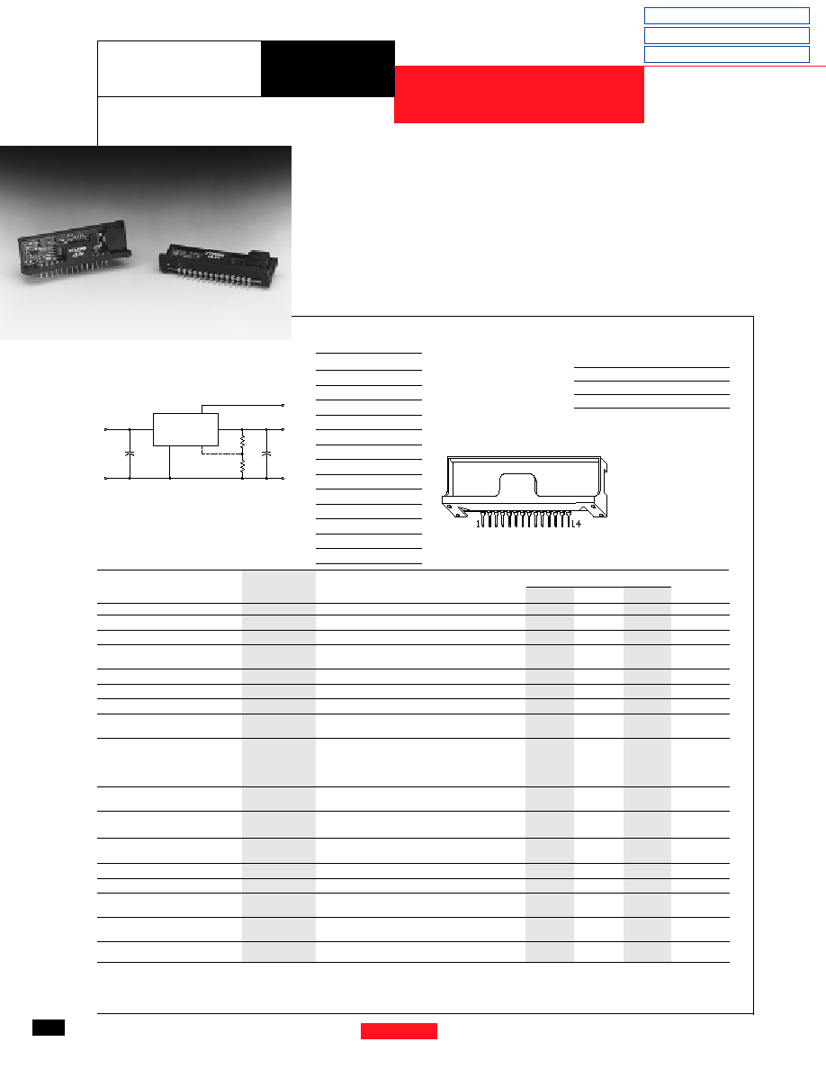
Standard Application
C
1
= Required 100µF electrolytic
C
2
= Required 100µF electrolytic
Ordering Information
PT6424
® = +1.5 Volts
PT6425
® = +3.3 Volts
PT6426
® = +1.8 Volts
PT6427
® = +2.1 Volts
PT6428
® = +1.2 Volts
PT6429
® = +2.5 Volts
Pin-Out Information
Pin
Function
1
Remote Sense
2
Do not connect
3
Do not connect
4
V
in
5
V
in
6
V
in
7
GND
8
GND
9
GND
10
GND
11
V
out
12
V
out
13
V
out
14
V
out
Adjust
∑
Adjustable Output Voltage
∑
85% Efficiency
∑
Small SIP Footprint
∑
Input Voltage Range: 4.5V to 5.5V
∑
Remote Sense Capability
The PT6420 is a new addition to
the Power Trends high performance
+5V to +3.3V, 3Amp family of 14-Pin
SIP (Single In-line Package) Integrated
Switching Regulators (ISRs). Only two
external capacitors are required for
proper operation.
Please note that this product does
not include short circuit protection.
3 AMP ADJUSTABLE INTEGRATED
SWITCHING REGULATOR
P T 6 4 2 0
S e r i e s
PT Series Suffix
(PT1234
X
)
Case/Pin
Configuration
Vertical Through-Hole
P
Horizontal Through-Hole
D
Horizontal Surface Mount
E
PT6420
POWER TRENDS
Note: Back surface
of product is
conducting metal.
PT6420
C2
100µF
+
COM
V
OUT
4,5,6
7,8,9,10
11,12,13
14
C1
100µF
+
V
IN
COM
R1
(V
O
UP)
R2
(V
O
DOWN)
Remote
Sense
1
Pkg Style 310
Specifications
Characteristics
PT6420 SERIES
(T
a
= 25∞C unless noted)
Symbols
Conditions
Min
Typ
Max
Units
Output Current
I
o
4.5V
V
in
5.5V
0
--
3.0
A
Current Limit
I
cl
V
in
= +5V
--
3.6
5.0
A
Input Voltage Range
V
in
0.1A
I
o
3.0A
4.5
--
5.5
V
Output Voltage Tolerance
V
o
V
in
= +5V, I
o
= 3.0A
V
o
-0.05
3.3
V
o
+0.05
V
0∞C
T
a
+70∞C
Line Regulation
Reg
line
4.5V
V
in
5.5V, I
o
= 3.0A
--
±10
±25
mV
Load Regulation
Reg
load
V
in
= +5V, 0.3
I
o
3.0A
--
±10*
±25*
mV
V
o
Ripple/Noise
V
n
V
in
= 5V, I
o
= 3.0A
--
66
165
mVpp
Transient Response
t
tr
I
o
step between 1.5A and 3.0A
--
200
--
µSec
with C
2
= 100µF
V
os
V
o
over/undershoot
--
200
--
mV
Efficiency
V
in
= +5V, I
o
= 1.5A
V
o
= 3.3V
--
85
--
%
V
o
= 1.8V
--
74
--
%
V
o
= 2.1V
--
77
--
%
V
o
= 1.2V
--
63
--
%
Switching Frequency
o
4.5V
V
in
5.5V
500
650
800
kHz
0.3A
I
o
3.0A
Absolute Maximum
T
a
0
--
+85
∞C
Operating Temperature Range
Recommended Operating
T
a
Free Air Convection (40-60 LFM)
0
--
+70**
∞C
Temperature Range
At Vin= 5V, Io=2.5A
Thermal Resistance
ja
Free Air Convection (40-60 LFM)
--
25
--
∞C/W
Storage Temperature
T
s
--
-40
--
+125
∞C
Mechanical Shock
Per Mil-STD-883D, Method 2002.3 , 1 msec,
--
500
--
G's
Half Sine, mounted to a fixture
Mechanical Vibration
Per Mil-STD-883D, Method 2007.2,
20-2000 Hz, Soldered in a PC board
--
15
--
G's
Weight
--
--
--
6.5
--
grams
*When used with remote sense function.
**See Thermal Derating chart.
Note: The PT6420 Series requires two 100µF electrolytic or tantalum capacitors for proper operation in all applications.
For assistance or to order, call
(800) 531-5782
Power Trends, Inc.
27715 Diehl Road, Warrenville, IL 60555
(800) 531-5782
Fax: (630) 393-6902 http://
www.powertrends.com
27
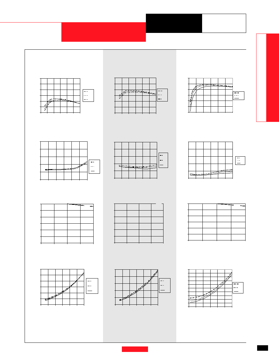
5V to 3.x Converters
5V Bus Products
DA
T
A
SHEETS
C H A R A C T E R I S T I C D A T A
0
0.5
1
1.5
2
2.5
3
4.5
4.75
5
5.25
5.5
PT6427, 2.1 VDC
(See Note 1)
Efficiency vs Output Current
Ripple vs Output Current
Power Dissipation vs Output Current
Note 1:
Note 1:
Note 1:
Note 1:
Note 1:
All data listed in the above graphs except for derating data has been developed from actual products tested at 25∞C. This data is considered typical data for the ISR.
Note 2:
Thermal derating graphs are developed in free air convection cooling of 40-60 LFM. (See Thermal Application Notes.)
40
50
60
70
80
90
100
0
0.5
1
1.5
2
2.5
3
4.5V
5.0V
5.5V
Vin
0
0.2
0.4
0.6
0.8
1
1.2
1.4
1.6
1.8
2
0
0.5
1
1.5
2
2.5
3
5.5V
5.0V
4.5V
Vin
Efficiency - %
Ripple-(mV)
PD-(W
atts)
Iout-(Amps)
Iout-(Amps)
Iout-(Amps)
P T 6 4 2 0
S e r i e s
Thermal Derating (T
a
)
(See Note 2)
Iout-(Amps)
Vin-(Volts)
Efficiency vs Output Current
Ripple vs Output Current
Power Dissipation vs Output Current
Efficiency - %
Ripple-(mV)
PD-(W
atts)
Iout-(Amps)
Iout-(Amps)
Iout-(Amps)
Thermal Derating (T
a
)
(See Note 2)
Iout-(Amps)
Vin-(Volts)
PT6425, 3.3 VDC
(See Note 1)
Efficiency vs Output Current
Ripple vs Output Current
Power Dissipation vs Output Current
Efficiency - %
Ripple-(mV)
PD-(W
atts)
Iout-(Amps)
Iout-(Amps)
Iout-(Amps)
Thermal Derating (T
a
)
(See Note 2)
Iout-(Amps)
Vin-(Volts)
PT6428 1.2 VDC
(See Note 1)
0
0.5
1
1.5
2
2.5
3
4.5
4 .7 5
5
5 .2 5
5.5
4 0
5 0
6 0
7 0
8 0
9 0
10 0
0.0
0.5
1.0
1.5
2.0
2.5
3.0
4.5V
5.0V
5.5V
Vin
85∞C
0.0
0.5
1.0
1.5
2.0
2.5
3.0
0.0
0.5
1.0
1.5
2.0
2.5
3.0
5.5V
5.0V
4.5V
Vin
0
20
40
60
80
100
0
0.5
1
1.5
2
2.5
3
5 .5V
5 .0V
4 .5V
V in
4 0
5 0
6 0
7 0
8 0
9 0
10 0
0
0.5
1
1.5
2
2.5
3
4.5 V
5.0 V
5.5 V
V in
0
0.5
1
1.5
2
2.5
3
4.5
4.75
5
5.25
5.5
85∞C
0
0.5
1
1.5
2
2.5
0
0.5
1
1.5
2
2.5
3
5 .5 V
5 .0 V
4 .5 V
Vin
0
2 0
4 0
6 0
8 0
10 0
0
0.5
1
1.5
2
2.5
3
5.5V
5.0V
4.5V
Vin
85∞C
0
20
40
60
80
100
0
0.5
1
1.5
2
2.5
3
5.5V
5.0V
4.5V
Vin
For assistance or to order, call
(800) 531-5782
3
Power Trends, Inc.
27715 Diehl Road, Warrenville, IL 60555
(800) 531-5782
Fax: (630) 393-6902 http://www.powertrends.com
A p p l i c a t i o n
N o t e s
PT6420 Series
More Applcation Notes
Adjusting the Output Voltage of the PT6420 Series
3AMP 5V Bus Converters
The output voltage of the Power Trends PT6420 Series ISRs
may be adjusted higher or lower than the factory trimmed pre-
set voltage with the addition of a single external resistor. Table 1
accordingly gives the allowable adjustment range for each model
in the series as V
a
(min) and V
a
(max).
Adjust Up:
(See note 1)
An increase in the output voltage is obtained by adding a resistor
R1, between pin 14 (V
o
adjust) and pins 11-13 (V
out
).
Adjust Down:
(See note 1)
Add a resistor
(R2)
, between pin 14 (V
o
adjust) and pins 7-10
(GND).
Refer to Figure 1 and Table 2 for both the placement and value
of the required resistor; either R1 or
(R2)
as appropriate.
Notes:
1. The direction in which each resistor adjusts the output of the
PT6420 series differs from many other Power Trends prod-
ucts. These output voltage adjustment notes are therefore
specific only to the PT6420 models.
2. Use only a single 1% resistor in either the R1 or
(R2)
loca-
tion. Place the resistor as close to the ISR as possible.
3. Never connect capacitors from V
o
adjust to either GND,
V
out
, or the Remote Sense pin. Any capacitance added to
the V
o
adjust pin will affect the stability of the ISR.
4. The PT6420 incorporates a Remote Sense (See Figure 1).
If this feature is being used, connecting the resistor R1
between pin 14 (V
o
adjust) and pin 1 (Remote Sense) can
benefit load regulation.
5. An increase in the output voltage may place additional limits
on the input voltage range of the part. The revised mini-
mum input voltage will be (V
out
+ 1.2) or 4.5V, whichever is
higher. Do not exceed 5.5Vdc.
Table 1
PT6420 ADJUSTMENT RANGE
Series Pt #
PT6428
PT6424
PT6426
PT6427
PT6429
PT6425
Vo (nom)
1.2
1.5
1.8
2.1
2.5
3.3
Va (min)
1.1
1.3
1.5
1.8
2.1
2.8
Va (max)
1.4
1.8
2.2
2.6
3.1
3.8
Figure 1
R 1
Adjust Up
C 1
100
µ
F
C 2
100
µ
F
Vo
C O M
C O M
Vin
+
+
(R2)
Adj Down
L
O
A
D
PT6420
1 1 , 1 2 , 1 3
1 4
7 , 8 , 9 , 1 0
4 , 5 , 6
V i n
V o
G N D
Vo(adj)
1
V s e n s e
The values of R1 [adjust up], and
(R2)
[adjust down], can
also be calculated using the following formulae.
12.45 V
o
R1
=
(V
a
≠ V
o
)
≠ 49.9
k
12.45 (2V
a
≠ V
o
)
≠ 49.9 k
(R2)
=
V
o
≠ V
a
Where:
V
o
= Original output voltage
V
a
= Adjusted output voltage
For assistance or to order, call
(800) 531-5782
4
A p p l i c a t i o n
Power Trends, Inc.
27715 Diehl Road, Warrenville, IL 60555
(800) 531-5782
Fax: (630) 393-6902 http://www.powertrends.com
N o t e s
PT6420 Series
Table 2
PT6420 ADJUSTMENT RESISTOR VALUES
Series Pt #
PT6428
PT6424
PT6426
PT6427
PT6429
PT6425
V
o
(nom)
1.2
1.5
1.8
2.1
2.5
3.3
V
a
(req'd)
1.1
(74.6)k
1.15
(224.0)k
1.2
1.25
249.0k
1.3
99.5k
(18.6)k
1.35
49.7k
(49.7)k
1.4
24.8k
(112.0)k
1.45
(299.0)k
1.5
(0.0)k
1.55
324.0k
(14.8)k
1.6
137.0k
(37.3)k
1.65
74.6k
(74.6)k
1.7
43.5k
(149.0)k
1.75
24.8k
(373.0)k
1.8
12.4k
(12.4)k
1.85
398.0k
(29.8)k
1.9
174.0k
(55.9)k
1.95
99.5k
(99.5)k
2.0
62.2k
(187.0)k
2.05
39.7k
(448.0)k
2.1
24.8k
(3.0)k
2.15
14.1k
473.0k
(14.1)k
2.2
6.1k
212.0k
(29.0)k
2.25
124.0k
(49.7)k
2.3
80.8k
(80.8)k
2.35
54.7k
(133.0)k
2.4
37.3k
(236.0)k
2.45
24.8k
(548.0)k
2.5
15.5k
2.55
8.2k
573.0k
2.6
2.4k
261.0k
2.65
158.0k
2.7
106.0k
2.75
74.6k
2.8
53.9k
(7.4)k
2.85
39.0k
(16.5)k
2.9
27.9k
(27.9)k
2.95
19.3k
(42.6)k
3.0
12.4k
(62.2)k
3.1
2.0k
(131.0)k
3.2
(336.0)k
3.3
3.4
361.0k
3.5
156.0k
3.6
87.0k
3.7
52.8k
3.8
32.3k
R1 = Black
R2 =
(Red)

IMPORTANT NOTICE
Texas Instruments and its subsidiaries (TI) reserve the right to make changes to their products or to discontinue
any product or service without notice, and advise customers to obtain the latest version of relevant information
to verify, before placing orders, that information being relied on is current and complete. All products are sold
subject to the terms and conditions of sale supplied at the time of order acknowledgement, including those
pertaining to warranty, patent infringement, and limitation of liability.
TI warrants performance of its semiconductor products to the specifications applicable at the time of sale in
accordance with TI's standard warranty. Testing and other quality control techniques are utilized to the extent
TI deems necessary to support this warranty. Specific testing of all parameters of each device is not necessarily
performed, except those mandated by government requirements.
CERTAIN APPLICATIONS USING SEMICONDUCTOR PRODUCTS MAY INVOLVE POTENTIAL RISKS OF
DEATH, PERSONAL INJURY, OR SEVERE PROPERTY OR ENVIRONMENTAL DAMAGE ("CRITICAL
APPLICATIONS"). TI SEMICONDUCTOR PRODUCTS ARE NOT DESIGNED, AUTHORIZED, OR
WARRANTED TO BE SUITABLE FOR USE IN LIFE-SUPPORT DEVICES OR SYSTEMS OR OTHER
CRITICAL APPLICATIONS. INCLUSION OF TI PRODUCTS IN SUCH APPLICATIONS IS UNDERSTOOD TO
BE FULLY AT THE CUSTOMER'S RISK.
In order to minimize risks associated with the customer's applications, adequate design and operating
safeguards must be provided by the customer to minimize inherent or procedural hazards.
TI assumes no liability for applications assistance or customer product design. TI does not warrant or represent
that any license, either express or implied, is granted under any patent right, copyright, mask work right, or other
intellectual property right of TI covering or relating to any combination, machine, or process in which such
semiconductor products or services might be or are used. TI's publication of information regarding any third
party's products or services does not constitute TI's approval, warranty or endorsement thereof.
Copyright
©
1999, Texas Instruments Incorporated