 | –≠–ª–µ–∫—Ç—Ä–æ–Ω–Ω—ã–π –∫–æ–º–ø–æ–Ω–µ–Ω—Ç: RC4136NS | –°–∫–∞—á–∞—Ç—å:  PDF PDF  ZIP ZIP |
RC4136, RM4136, RV4136
QUAD GENERAL-PURPOSE OPERATIONAL AMPLIFIERS
SLOS072A ≠ MARCH 1978 ≠ REVISED JANUARY 2002
1
POST OFFICE BOX 655303
∑
DALLAS, TEXAS 75265
D
Continuous Short-Circuit Protection
D
Wide Common-Mode and Differential
Voltage Ranges
D
No Frequency Compensation Required
D
Low Power Consumption
D
No Latch-Up
D
Unity-Gain Bandwidth . . . 3 MHz Typ
D
Gain and Phase Match Between Amplifiers
D
Designed To Be Interchangeable With
Raytheon RC4136, RM4136, and RV4136
D
Low Noise . . . 8 nV
Hz Typ at 1 kHz
description
The RC4136, RM4136, and RV4136 are quad
general-purpose operational amplifiers, with each
amplifier electrically similar to the
µ
A741, except
that offset null capability is not provided.
The high common-mode input voltage range and
the absence of latch-up make these amplifiers
ideal for voltage-follower applications. The
devices are short-circuit protected and the
internal frequency compensation ensures stability
without external components.
The RC4136 is characterized for operation from
0
∞
C to 70
∞
C, the RM4136 is characterized for
operation over the full military temperature range
of ≠55
∞
C to 125
∞
C, and the RV4136 is
characterized for operation from ≠40
∞
C to 85
∞
C.
symbol (each amplifier)
+
≠
IN+
IN≠
OUT
AVAILABLE OPTIONS
VIOMAX
PACKAGE
TA
VIOMAX
AT 25
∞
C
SMALL OUTLINE
CHIP CARRIER
CERAMIC DIP
PLASTIC DIP
FLAT
AT 25 C
(D)
(FK)
(J)
(N)
(W)
0
∞
C to 70
∞
C
6 mV
RC4136D
--
--
RC4136N
--
≠40
∞
C to 85
∞
C
6 mV
RV4136D
--
--
RV4136N
--
≠55
∞
C to 125
∞
C
4 mV
--
RM4136FK
RM4136J
--
RM4136W
The D packages are available taped and reeled. Add the suffix R to the device type (e.g., RC4136DR).
The RM4136 and RV4136 are
obsolete and are no longer supplied.
Copyright
2002, Texas Instruments Incorporated
PRODUCTION DATA information is current as of publication date.
Products conform to specifications per the terms of Texas Instruments
standard warranty. Production processing does not necessarily include
testing of all parameters.
Please be aware that an important notice concerning availability, standard warranty, and use in critical applications of
Texas Instruments semiconductor products and disclaimers thereto appears at the end of this data sheet.
1
2
3
4
5
6
7
14
13
12
11
10
9
8
1IN≠
1IN+
1OUT
2OUT
2IN+
2IN≠
V
CC≠
4IN≠
4IN+
4OUT
V
CC+
3OUT
3IN+
3IN≠
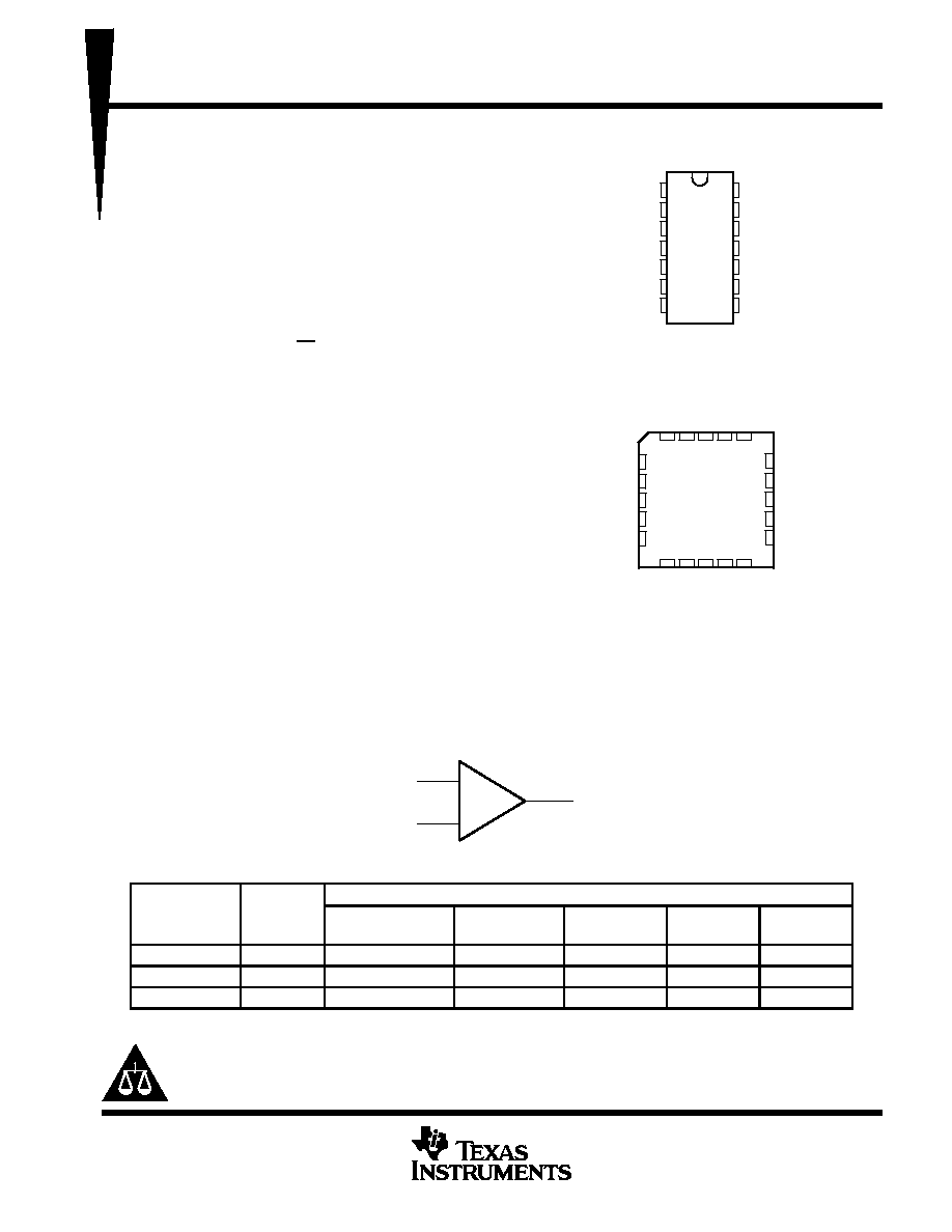
RM4136 . . . J OR W PACKAGE
ALL OTHERS . . . D OR N PACKAGE
(TOP VIEW)
3
2
1 20 19
9 10 11 12 13
4
5
6
7
8
18
17
16
15
14
4OUT
NC
V
CC+
NC
3OUT
1OUT
NC
2OUT
NC
2IN+
RM4136 . . . FK PACKAGE
(TOP VIEW)
NC
3IN≠
3IN+
2IN≠
NC
1IN+
1IN≠
4IN≠
4IN+
V
CC≠
NC ≠ No internal connection
On products compliant to MIL-PRF-38535, all parameters are tested
unless otherwise noted. On all other products, production
processing does not necessarily include testing of all parameters.
RC4136, RM4136, RV4136
QUAD GENERAL-PURPOSE OPERATIONAL AMPLIFIERS
SLOS072A ≠ MARCH 1978 ≠ REVISED JANUARY 2002
2
POST OFFICE BOX 655303
∑
DALLAS, TEXAS 75265
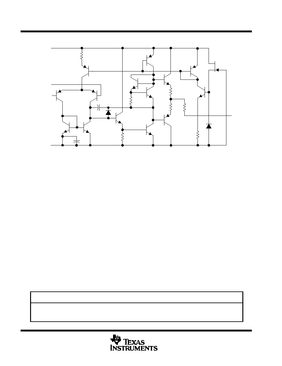
schematic (each amplifier)
OUT
IN+
IN≠
VCC≠
VCC+
absolute maximum ratings over operating free-air temperature range (unless otherwise noted)
Supply voltage (see Note 1): V
CC+,
RC4136 and RV4136
18 V
. . . . . . . . . . . . . . . . . . . . . . . . . . . . . . . . . . . . . . .
V
CC+,
RM4136 22
V
. . . . . . . . . . . . . . . . . . . . . . . . . . . . . . . . . . . . . . . . . . . . . . . . . .
V
CC≠,
RC4136 and RV4136
≠18 V
. . . . . . . . . . . . . . . . . . . . . . . . . . . . . . . . . . . . . .
V
CC≠,
RM4136
≠22 V
. . . . . . . . . . . . . . . . . . . . . . . . . . . . . . . . . . . . . . . . . . . . . . . . .
Differential input voltage, V
ID
(see Note 2)
±
30
V
. . . . . . . . . . . . . . . . . . . . . . . . . . . . . . . . . . . . . . . . . . . . . . . . . . .
Input voltage, V
I
(any input) (see Notes 1 and 3)
±
15 V
. . . . . . . . . . . . . . . . . . . . . . . . . . . . . . . . . . . . . . . . . . . . . .
Duration of output short circuit to ground, one amplifier at a time (see Note 4)
Unlimited
. . . . . . . . . . . . . . . . .
Continuous total dissipation
See Dissipation Rating Table
. . . . . . . . . . . . . . . . . . . . . . . . . . . . . . . . . . . . . . . . . . .
Package thermal impedance,
JA
(see Note 5): D package
86
∞
C/W
. . . . . . . . . . . . . . . . . . . . . . . . . . . . . . . . . . .
N package
80
∞
C/W
. . . . . . . . . . . . . . . . . . . . . . . . . . . . . . . . . . .
Case temperature for 60 seconds: FK package
260
∞
C
. . . . . . . . . . . . . . . . . . . . . . . . . . . . . . . . . . . . . . . . . . . . . .
Lead temperature 1,6 mm (1/16 inch) from case for 10 seconds: D or N package
260
∞
C
. . . . . . . . . . . . . . . .
Lead temperature 1,6 mm (1/16 inch) from case for 60 seconds: J or W package
300
∞
C
. . . . . . . . . . . . . . . .
Storage temperature range, T
stg
≠65
∞
C to 150
∞
C
. . . . . . . . . . . . . . . . . . . . . . . . . . . . . . . . . . . . . . . . . . . . . . . . . . .
Stresses beyond those listed under "absolute maximum ratings" may cause permanent damage to the device. These are stress ratings only, and
functional operation of the device at these or any other conditions beyond those indicated under "recommended operating conditions" is not
implied. Exposure to absolute-maximum-rated conditions for extended periods may affect device reliability.
NOTES:
1. All voltage values, unless otherwise noted, are with respect to the midpoint between VCC+ and VCC≠.
2. Differential voltages are at IN+ with respect to IN≠.
3. The magnitude of the input voltage must never exceed the magnitude of the supply voltage or 15 V, whichever is less.
4. Temperature and/or supply voltages must be limited to ensure that the dissipation rating is not exceeded.
5. The package thermal impedance is calculated in accordance with JESD 51-7.
DISSIPATION RATING TABLE
PACKAGE
TA
25
∞
C
POWER RATING
DERATING
FACTOR
DERATE
ABOVE TA
TA = 70
∞
C
POWER RATING
TA = 85
∞
C
POWER RATING
TA = 125
∞
C
POWER RATING
FK
800 mW
11.0 mW/
∞
C
77
∞
C
800 mW
715 mW
275 mW
J
800 mW
11.0 mW/
∞
C
77
∞
C
800 mW
715 mW
275 mW
W
800 mW
8.0 mW/
∞
C
50
∞
C
640 mW
520 mW
200 mW
The RM4136 and RV4136 are
obsolete and are no longer supplied.
RC4136, RM4136, RV4136
QUAD GENERAL-PURPOSE OPERATIONAL AMPLIFIERS
SLOS072A ≠ MARCH 1978 ≠ REVISED JANUARY 2002
3
POST OFFICE BOX 655303
∑
DALLAS, TEXAS 75265
recommended operating conditions
MIN
MAX
UNIT
VCC+
Supply voltage
5
15
V
VCC≠
Supply voltage
≠5
≠15
V
electrical characteristics at specified free-air temperature, V
CC+
= 15 V, V
CC≠
= ≠15 V
PARAMETER
TEST CONDITIONS
RC4136
RM4136
RV4136
UNIT
PARAMETER
TEST CONDITIONS
MIN
TYP
MAX
MIN
TYP
MAX
MIN
TYP
MAX
UNIT
Input offset
25
∞
C
0.5
6
0.5
4
0.5
6
VIL
Input offset
voltage
VO = 0
Full
range
7.5
6
7.5
mV
Input offset
25
∞
C
5
200
5
150
5
200
IIO
Input offset
current
VO = 0
Full
range
300
500
500
nA
25
∞
C
140
500
140
400
140
500
IIB
Input bias current
VO = 0
Full
range
800
1500
1500
nA
Vi
Input voltage
range
25
∞
C
±
12
±
14
±
12
±
14
±
12
±
14
V
Maximum peak
RL = 10 k
25
∞
C
±
12
±
14
±
12
±
14
±
12
±
14
VOM
Maximum peak
output voltage
RL = 2 k
25
∞
C
±
10
±
13
±
10
±
13
±
10
±
13
V
VOM
out ut voltage
swing
RL
2 k
Full
range
±
10
±
10
±
10
V
Large-signal
VO =
±
10 V
25
∞
C
20
300
50
350
20
300
AVD
g
g
differential voltage
amplification
VO =
±
10 V,
RL
2 k
Full
range
15
25
15
V/mV
B1
Unity-gain
bandwidth
25
∞
C
3
3.5
3
MHz
ri
Input resistance
25
∞
C
0.3
*
5
0.3
*
5
0.3
*
5
M
CMRR
Common-mode
rejection ratio
VO = 0,
RS = 50
25
∞
C
70
90
70
90
70
90
dB
Supply-voltage
VCC =
±
9 V to
±
15 V
kSVS
y
g
sensitivity
VCC =
±
9 V to
±
15 V,
VO = 0
25
∞
C
30
150
30
150
30
150
µ
V/V
SVS
(
VIO/
VCC)
VO = 0
µ
Vn
Equivalent input
noise voltage
(closed loop)
AVD = 100,
BW = 1 Hz,
f = 1 kHz,
RS = 100
25
∞
C
8
8
8
nV
Hz
Supply current
25
∞
C
5
11.3
5
11.3
5
11.3
ICC
Supply current
(all four amplifiers)
VO = 0,
No load
MIN TA
6
13.7
6
13.3
6
13.7
mA
(all four am lifiers)
MAX TA
4.5
10
4.5
10
4.5
10
Total power
25
∞
C
150
340
150
340
150
340
PD
Total ower
dissipation
VO = 0,
No load
MIN TA
180
400
180
400
180
400
mW
(all four amplifiers)
MAX TA
135
300
135
300
135
300
Crosstalk
AVD = 100,
attenuation
VD
,
f = 10 kHz,
25
∞
C
105
105
105
dB
(VO1/VO2)
RS = 1 k
*
This parameter is not production tested.
All characteristics are measured under open-loop conditions with zero common-mode input voltage, unless otherwise specified. Full range is
0
∞
C to 70
∞
C for RC4136, ≠55
∞
C to 125
∞
C for RM4136, and ≠40
∞
C to 85
∞
C for RV4136. Minimum TA is 0
∞
C for RC4136, ≠55
∞
C for RM4136, and
≠40
∞
C for RV4136. Maximum TA is 70
∞
C for RC4136, 125
∞
C for RM4136, and 85
∞
C for RV4136.
The RM4136 and RV4136 are
obsolete and are no longer supplied.
RC4136, RM4136, RV4136
QUAD GENERAL-PURPOSE OPERATIONAL AMPLIFIERS
SLOS072A ≠ MARCH 1978 ≠ REVISED JANUARY 2002
4
POST OFFICE BOX 655303
∑
DALLAS, TEXAS 75265
operating characteristics, V
CC+
= 15 V, V
CC≠
= ≠15 V, T
A
= 25
∞
C
PARAMETER
TEST CONDITIONS
TYP
UNIT
tr
Rise time
VI = 20 mV,
CL = 100 pF, RL = 2 k
0.13
µ
s
Overshoot factor
VI = 20 mV,
CL = 100 pF, RL = 2 k
5
%
SR
Slew rate at unity gain
VI = 10 V
CL = 100 pF
RL = 2 k
1 7
V/
µ
s
SR
Slew rate at unity gain
VI = 10 V,
CL = 100 pF, RL = 2 k
1.7
V/
µ
s
The RM4136 and RV4136 are
obsolete and are no longer supplied.

IMPORTANT NOTICE
Texas Instruments Incorporated and its subsidiaries (TI) reserve the right to make corrections, modifications,
enhancements, improvements, and other changes to its products and services at any time and to discontinue
any product or service without notice. Customers should obtain the latest relevant information before placing
orders and should verify that such information is current and complete. All products are sold subject to TI's terms
and conditions of sale supplied at the time of order acknowledgment.
TI warrants performance of its hardware products to the specifications applicable at the time of sale in
accordance with TI's standard warranty. Testing and other quality control techniques are used to the extent TI
deems necessary to support this warranty. Except where mandated by government requirements, testing of all
parameters of each product is not necessarily performed.
TI assumes no liability for applications assistance or customer product design. Customers are responsible for
their products and applications using TI components. To minimize the risks associated with customer products
and applications, customers should provide adequate design and operating safeguards.
TI does not warrant or represent that any license, either express or implied, is granted under any TI patent right,
copyright, mask work right, or other TI intellectual property right relating to any combination, machine, or process
in which TI products or services are used. Information published by TI regarding third≠party products or services
does not constitute a license from TI to use such products or services or a warranty or endorsement thereof.
Use of such information may require a license from a third party under the patents or other intellectual property
of the third party, or a license from TI under the patents or other intellectual property of TI.
Reproduction of information in TI data books or data sheets is permissible only if reproduction is without
alteration and is accompanied by all associated warranties, conditions, limitations, and notices. Reproduction
of this information with alteration is an unfair and deceptive business practice. TI is not responsible or liable for
such altered documentation.
Resale of TI products or services with statements different from or beyond the parameters stated by TI for that
product or service voids all express and any implied warranties for the associated TI product or service and
is an unfair and deceptive business practice. TI is not responsible or liable for any such statements.
Mailing Address:
Texas Instruments
Post Office Box 655303
Dallas, Texas 75265
Copyright
2002, Texas Instruments Incorporated