 | –≠–ª–µ–∫—Ç—Ä–æ–Ω–Ω—ã–π –∫–æ–º–ø–æ–Ω–µ–Ω—Ç: RC4558IDR | –°–∫–∞—á–∞—Ç—å:  PDF PDF  ZIP ZIP |
RC4558
DUAL GENERAL PURPOSE OPERATIONAL AMPLIFIER
SLOS073D - MARCH 1976 - REVISED SEPTEMBER 2004
1
POST OFFICE BOX 655303
∑
DALLAS, TEXAS 75265
D
Continuous Short-Circuit Protection
D
Wide Common-Mode and Differential
Voltage Ranges
D
No Frequency Compensation Required
D
Low Power Consumption
D
No Latch-Up
D
Unity-Gain Bandwidth . . . 3 MHz Typ
D
Gain and Phase Match Between Amplifiers
D
Low Noise . . . 8 nV/
Hz Typ at 1 kHz
description/ordering information
The RC4558 device is a dual general-purpose operational amplifier, with each half electrically similar to the
µ
A741, except that offset null capability is not provided.
The high common-mode input voltage range and the absence of latch-up make this amplifier ideal for
voltage-follower applications. The device is short-circuit protected, and the internal frequency compensation
ensures stability without external components.
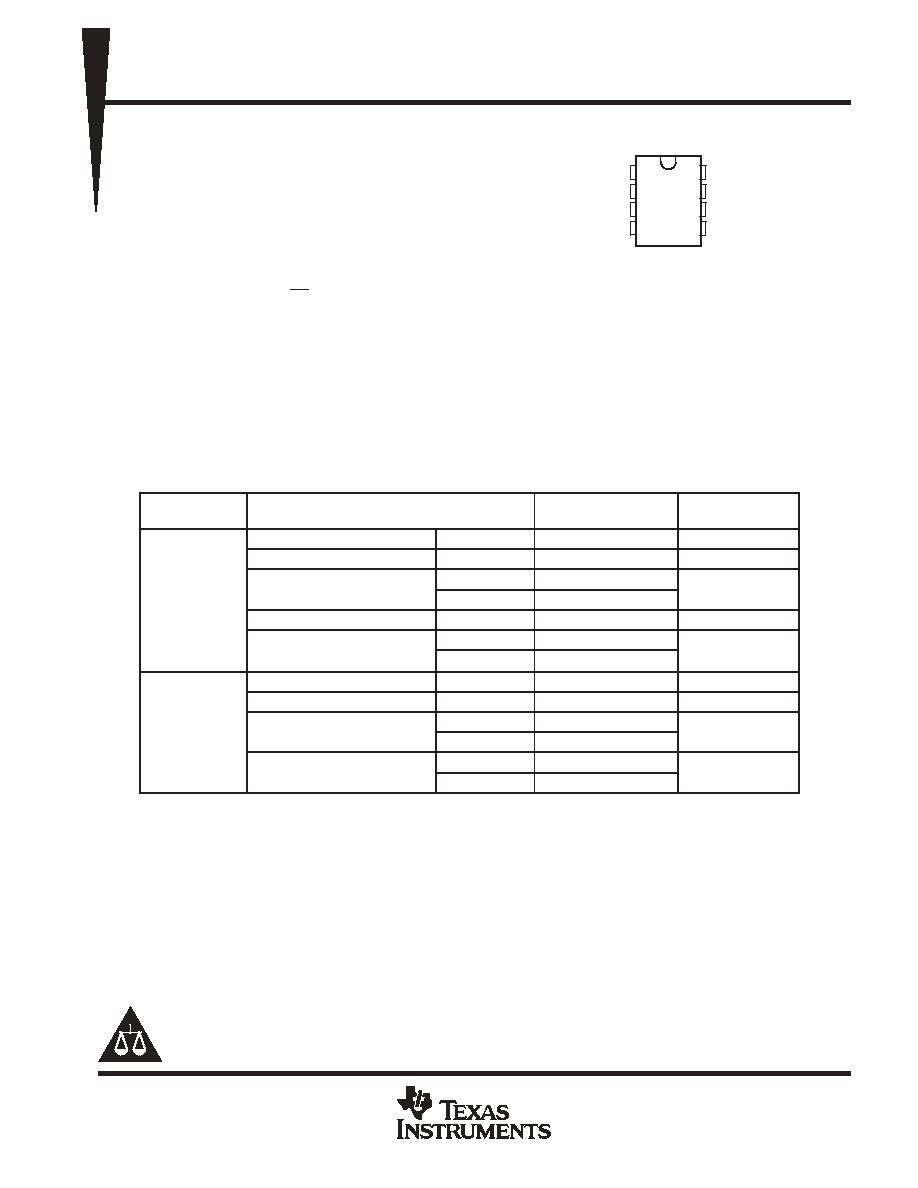
ORDERING INFORMATION
TA
PACKAGE
ORDERABLE
PART NUMBER
TOP-SIDE
MARKING
MSOP/VSSOP (DGK)
Reel of 2500
RC4558DGKR
YR_
PDIP (P)
Tube of 50
RC4558P
RC4558P
SOIC (D)
Tube of 75
RC4558D
RC4558
0
∞
C to 70
∞
C
SOIC (D)
Reel of 2500
RC4558DR
RC4558
0 C to 70 C
SOP (PS)
Reel of 2000
RC4558PSR
R4558
TSSOP (PW)
Tube of 150
RC4558PW
R4558
TSSOP (PW)
Reel of 2000
RC4558PWR
R4558
MSOP/VSSOP (DGK)
Reel of 2500
RC4558IDGKR
YS_
PDIP (P)
Tube of 50
RC4558IP
RC4558IP
-40
∞
C to 85
∞
C
SOIC (D)
Tube of 75
RC4558ID
R4558I
-40
∞
C to 85
∞
C
SOIC (D)
Reel of 2500
RC4558IDR
R4558I
TSSOP (PW)
Tube of 150
RC4558IPW
R4558I
TSSOP (PW)
Reel of 2000
RC4558IPWR
R4558I
Package drawings, standard packing quantities, thermal data, symbolization, and PCB design guidelines are available at
www.ti.com/sc/package.
The actual top-side marking has one additional character that designates the assembly/test site.
Copyright
2004, Texas Instruments Incorporated
PRODUCTION DATA information is current as of publication date.
Products conform to specifications per the terms of Texas Instruments
standard warranty. Production processing does not necessarily include
testing of all parameters.
1
2
3
4
8
7
6
5
1OUT
1IN-
1IN+
V
CC
-
V
CC
+
2OUT
2IN-
2IN+
D, DGK, P, PS, OR PW PACKAGE
(TOP VIEW)
Please be aware that an important notice concerning availability, standard warranty, and use in critical applications of
Texas Instruments semiconductor products and disclaimers thereto appears at the end of this data sheet.
RC4558
DUAL GENERAL PURPOSE OPERATIONAL AMPLIFIER
SLOS073D - MARCH 1976 - REVISED SEPTEMBER 2004
2
POST OFFICE BOX 655303
∑
DALLAS, TEXAS 75265
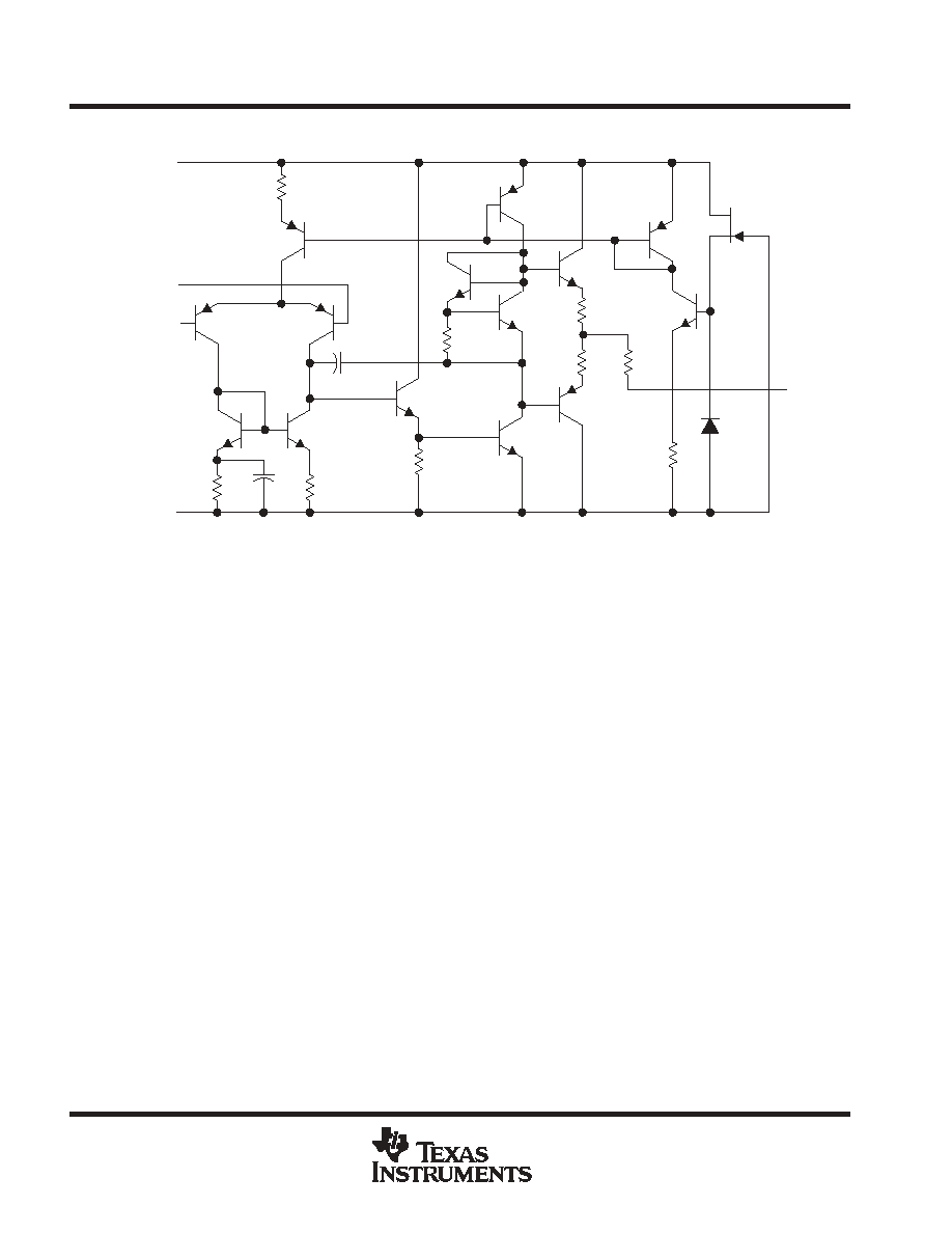
schematic (each amplifier)
OUT
IN+
IN-
VCC-
VCC+
absolute maximum ratings over operating free-air temperature range (unless otherwise noted)
Supply voltage
(see Note 1): V
CC+
18
V
. . . . . . . . . . . . . . . . . . . . . . . . . . . . . . . . . . . . . . . . . . . . . . . . . . . . . . . . . .
V
CC-
-18
V
. . . . . . . . . . . . . . . . . . . . . . . . . . . . . . . . . . . . . . . . . . . . . . . . . . . . . . . . .
Differential input voltage, V
ID
(see Note 2)
±
30 V
. . . . . . . . . . . . . . . . . . . . . . . . . . . . . . . . . . . . . . . . . . . . . . . . . . .
Input voltage, V
I
(any input, see Notes 1 and 3)
±
15 V
. . . . . . . . . . . . . . . . . . . . . . . . . . . . . . . . . . . . . . . . . . . . . . .
Duration of output short circuit to ground, one amplifier at a time (see Note 4)
Unlimited
. . . . . . . . . . . . . . . . .
Package thermal impedance,
JA
(see Notes 5 and 6): D package
97
∞
C/W
. . . . . . . . . . . . . . . . . . . . . . . . . . . .
DGK package
172
∞
C/W
. . . . . . . . . . . . . . . . . . . . . . . .
P package
85
∞
C/W
. . . . . . . . . . . . . . . . . . . . . . . . . . . .
PS package
95
∞
C/W
. . . . . . . . . . . . . . . . . . . . . . . . . . .
PW package
149
∞
C/W
. . . . . . . . . . . . . . . . . . . . . . . . .
Operating virtual junction temperature, T
J
150
∞
C
. . . . . . . . . . . . . . . . . . . . . . . . . . . . . . . . . . . . . . . . . . . . . . . . . . .
Storage temperature range, T
stg
-65
∞
C to 150
∞
C
. . . . . . . . . . . . . . . . . . . . . . . . . . . . . . . . . . . . . . . . . . . . . . . . . . .
Stresses beyond those listed under "absolute maximum ratings" may cause permanent damage to the device. These are stress ratings only, and
functional operation of the device at these or any other conditions beyond those indicated under "recommended operating conditions" is not
implied. Exposure to absolute-maximum-rated conditions for extended periods may affect device reliability.
NOTES:
1. All voltage values, unless otherwise noted, are with respect to the midpoint between VCC+ and VCC-.
2. Differential voltages are at IN+ with respect to IN-.
3. The magnitude of the input voltage must never exceed the magnitude of the supply voltage or 15 V, whichever is less.
4. Temperature and/or supply voltages must be limited to ensure that the dissipation rating is not exceeded.
5. Maximum power dissipation is a function of TJ(max),
JA, and TA. The maximum allowable power dissipation at any allowable
ambient temperature is PD = (TJ(max) - TA)/
JA. Operating at the absolute maximum TJ of 150
∞
C can affect reliability.
6. The package thermal impedance is calculated in accordance with JESD 51-7.

RC4558
DUAL GENERAL PURPOSE OPERATIONAL AMPLIFIER
SLOS073D - MARCH 1976 - REVISED SEPTEMBER 2004
3
POST OFFICE BOX 655303
∑
DALLAS, TEXAS 75265
recommended operating conditions
MIN
MAX
UNIT
VCC+
Supply voltage
5
15
V
VCC-
Supply voltage
-5
-15
V
TA
Operating free-air temperature
RC4558
0
70
∞
C
TA
Operating free-air temperature
RC4558I
-40
85
∞
C
electrical characteristics at specified free-air temperature, V
CC+
= 15 V, V
CC-
= -15 V
PARAMETER
TEST CONDITIONS
MIN
TYP
MAX
UNIT
25
∞
C
0.5
6
VIO
Input offset voltage
VO = 0
Full
range
7.5
mV
25
∞
C
5
200
IIO
Input offset current
VO = 0
Full
range
300
nA
25
∞
C
150
500
IIB
Input bias current
VO = 0
Full
range
800
nA
VICR
Common-mode input voltage range
25
∞
C
±
12
±
14
V
RL = 10 k
25
∞
C
±
12
±
14
VOM
Maximum output voltage swing
25
∞
C
±
10
±
13
V
VOM
Maximum output voltage swing
RL = 2 k
Full
range
±
10
V
RL
2 k
,
25
∞
C
20
300
AVD
Large-signal differential voltage amplification
RL
2 k
,
VO =
±
10 V
Full
range
15
V/mV
B1
Unity-gain bandwith
25
∞
C
3
MHz
ri
Input resistance
25
∞
C
0.3
5
M
CMRR
Common-mode rejection ratio
25
∞
C
70
90
dB
kSVS
Supply-voltage sensitivity (
VIO/
VCC)
VCC =
±
15 V
to
±
9 V
25
∞
C
30
150
µ
V/V
Vn
Equivalent input noise voltage (closed loop)
AVD = 100,
RS = 100
,
f = 1 kHz,
BW = 1 Hz
25
∞
C
8
nV/
Hz
VO = 0,
25
∞
C
2.5
5.6
ICC
Supply current (both amplifiers)
VO = 0,
No load
TA(min)
3
6.6
mA
ICC
Supply current (both amplifiers)
No load
TA(max)
2.3
5
mA
Total power dissipation
VO = 0,
25
∞
C
75
170
PD
Total power dissipation
(both amplifiers)
VO = 0,
No load
TA(min)
90
200
mW
PD
(both amplifiers)
No load
TA(max)
70
150
mW
VO1/VO2
Crosstalk attenuation
Open loop
RS = 1 k
,
f = 10 kHz
25
∞
C
85
dB
VO1/VO2
Crosstalk attenuation
AVD = 100
RS = 1 k
,
f = 10 kHz
25
∞
C
105
dB
All characteristics are measured under open-loop conditions with zero common-mode input voltage, unless otherwise specified. Full range is
0
∞
C to 70
∞
C for RC4558 and -40
∞
C to 85
∞
C for RC4558I.
operating characteristics, V
CC+
= 15 V, V
CC-
= -15 V, T
A
= 25
∞
C
PARAMETER
TEST CONDITIONS
MIN
TYP
MAX
UNIT
tr
Rise time
VI = 20 mV,
RL = 2 k
,
CL = 100 pF
0.13
ns
Overshoot
VI = 20 mV,
RL = 2 k
,
CL = 100 pF
5
%
SR
Slew rate at unity gain
VI = 10 V,
RL = 2 k
,
CL = 100 pF
1.1
1.7
V/
µ
s
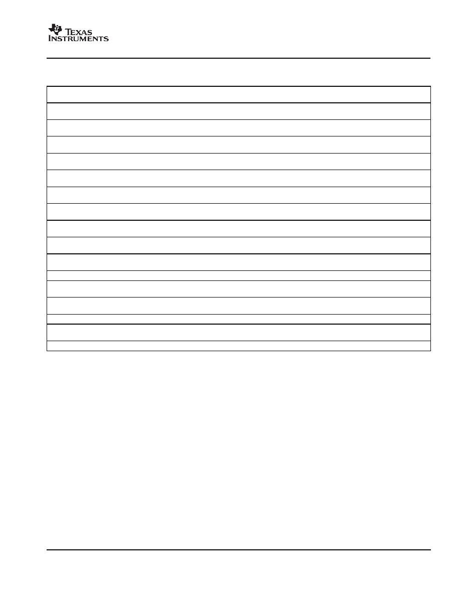
PACKAGING INFORMATION
Orderable Device
Status
(1)
Package
Type
Package
Drawing
Pins Package
Qty
Eco Plan
(2)
Lead/Ball Finish
MSL Peak Temp
(3)
RC4558D
ACTIVE
SOIC
D
8
75
Pb-Free
(RoHS)
CU NIPDAU
Level-2-260C-1 YEAR/
Level-1-235C-UNLIM
RC4558DGKR
ACTIVE
MSOP
DGK
8
2500 Green (RoHS &
no Sb/Br)
CU NIPDAU
Level-2-260C-1YEAR
RC4558DR
ACTIVE
SOIC
D
8
2500 Green (RoHS &
no Sb/Br)
CU NIPDAU
Level-1-260C-UNLIM
RC4558ID
ACTIVE
SOIC
D
8
75
Pb-Free
(RoHS)
CU NIPDAU
Level-2-260C-1 YEAR/
Level-1-235C-UNLIM
RC4558IDGKR
ACTIVE
MSOP
DGK
8
2500 Green (RoHS &
no Sb/Br)
CU NIPDAU
Level-2-260C-1YEAR
RC4558IDR
ACTIVE
SOIC
D
8
2500 Green (RoHS &
no Sb/Br)
CU NIPDAU
Level-1-260C-UNLIM
RC4558IP
ACTIVE
PDIP
P
8
50
Pb-Free
(RoHS)
CU NIPDAU
Level-NC-NC-NC
RC4558IPW
ACTIVE
TSSOP
PW
8
150
Pb-Free
(RoHS)
CU NIPDAU
Level-1-250C-UNLIM
RC4558IPWR
ACTIVE
TSSOP
PW
8
2000
Pb-Free
(RoHS)
CU NIPDAU
Level-1-250C-UNLIM
RC4558P
ACTIVE
PDIP
P
8
50
Pb-Free
(RoHS)
CU NIPDAU
Level-NC-NC-NC
RC4558PSLE
OBSOLETE
SO
PS
8
None
Call TI
Call TI
RC4558PSR
ACTIVE
SO
PS
8
2000
Pb-Free
(RoHS)
CU NIPDAU
Level-2-260C-1 YEAR/
Level-1-235C-UNLIM
RC4558PW
ACTIVE
TSSOP
PW
8
150
Pb-Free
(RoHS)
CU NIPDAU
Level-1-250C-UNLIM
RC4558PWLE
OBSOLETE
TSSOP
PW
8
None
Call TI
Call TI
RC4558PWR
ACTIVE
TSSOP
PW
8
2000
Pb-Free
(RoHS)
CU NIPDAU
Level-1-250C-UNLIM
RC4558Y
OBSOLETE
XCEPT
Y
0
None
Call TI
Call TI
(1)
The marketing status values are defined as follows:
ACTIVE: Product device recommended for new designs.
LIFEBUY: TI has announced that the device will be discontinued, and a lifetime-buy period is in effect.
NRND: Not recommended for new designs. Device is in production to support existing customers, but TI does not recommend using this part in
a new design.
PREVIEW: Device has been announced but is not in production. Samples may or may not be available.
OBSOLETE: TI has discontinued the production of the device.
(2)
Eco Plan - May not be currently available - please check
http://www.ti.com/productcontent
for the latest availability information and additional
product content details.
None: Not yet available Lead (Pb-Free).
Pb-Free (RoHS): TI's terms "Lead-Free" or "Pb-Free" mean semiconductor products that are compatible with the current RoHS requirements
for all 6 substances, including the requirement that lead not exceed 0.1% by weight in homogeneous materials. Where designed to be soldered
at high temperatures, TI Pb-Free products are suitable for use in specified lead-free processes.
Green (RoHS & no Sb/Br): TI defines "Green" to mean "Pb-Free" and in addition, uses package materials that do not contain halogens,
including bromine (Br) or antimony (Sb) above 0.1% of total product weight.
(3)
MSL, Peak Temp. -- The Moisture Sensitivity Level rating according to the JEDECindustry standard classifications, and peak solder
temperature.
Important Information and Disclaimer:The information provided on this page represents TI's knowledge and belief as of the date that it is
provided. TI bases its knowledge and belief on information provided by third parties, and makes no representation or warranty as to the
PACKAGE OPTION ADDENDUM
www.ti.com
18-Feb-2005
Addendum-Page 1

accuracy of such information. Efforts are underway to better integrate information from third parties. TI has taken and continues to take
reasonable steps to provide representative and accurate information but may not have conducted destructive testing or chemical analysis on
incoming materials and chemicals. TI and TI suppliers consider certain information to be proprietary, and thus CAS numbers and other limited
information may not be available for release.
In no event shall TI's liability arising out of such information exceed the total purchase price of the TI part(s) at issue in this document sold by TI
to Customer on an annual basis.
PACKAGE OPTION ADDENDUM
www.ti.com
18-Feb-2005
Addendum-Page 2
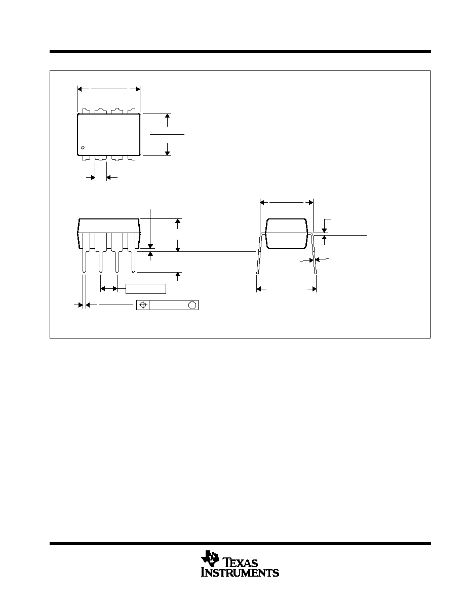
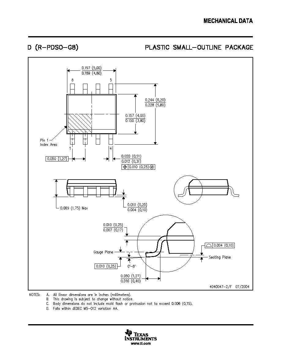
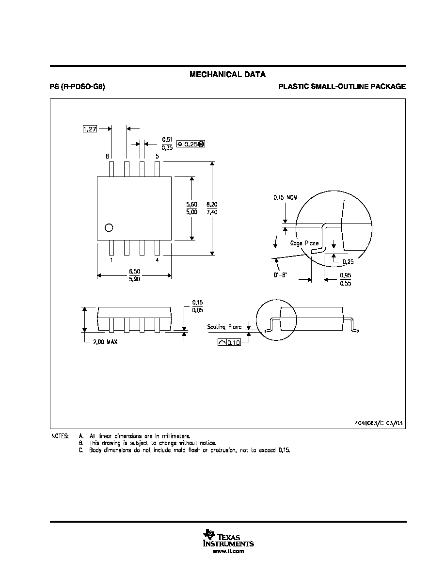
MECHANICAL DATA
MPDI001A ≠ JANUARY 1995 ≠ REVISED JUNE 1999
POST OFFICE BOX 655303
∑
DALLAS, TEXAS 75265
P (R-PDIP-T8)
PLASTIC DUAL-IN-LINE
8
4
0.015 (0,38)
Gage Plane
0.325 (8,26)
0.300 (7,62)
0.010 (0,25) NOM
MAX
0.430 (10,92)
4040082/D 05/98
0.200 (5,08) MAX
0.125 (3,18) MIN
5
0.355 (9,02)
0.020 (0,51) MIN
0.070 (1,78) MAX
0.240 (6,10)
0.260 (6,60)
0.400 (10,60)
1
0.015 (0,38)
0.021 (0,53)
Seating Plane
M
0.010 (0,25)
0.100 (2,54)
NOTES: A. All linear dimensions are in inches (millimeters).
B. This drawing is subject to change without notice.
C. Falls within JEDEC MS-001
For the latest package information, go to http://www.ti.com/sc/docs/package/pkg_info.htm

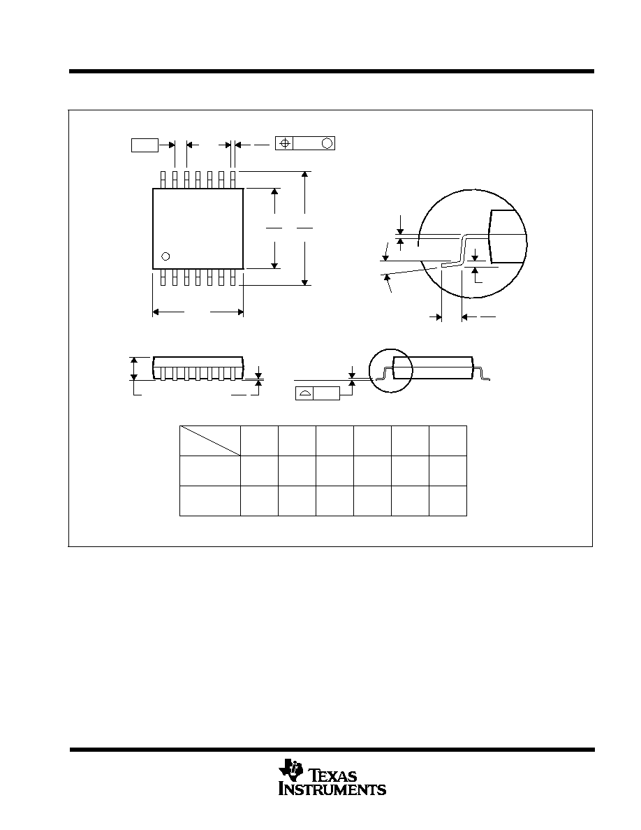
MECHANICAL DATA
MTSS001C ≠ JANUARY 1995 ≠ REVISED FEBRUARY 1999
POST OFFICE BOX 655303
∑
DALLAS, TEXAS 75265
PW (R-PDSO-G**)
PLASTIC SMALL-OUTLINE PACKAGE
14 PINS SHOWN
0,65
M
0,10
0,10
0,25
0,50
0,75
0,15 NOM
Gage Plane
28
9,80
9,60
24
7,90
7,70
20
16
6,60
6,40
4040064/F 01/97
0,30
6,60
6,20
8
0,19
4,30
4,50
7
0,15
14
A
1
1,20 MAX
14
5,10
4,90
8
3,10
2,90
A MAX
A MIN
DIM
PINS **
0,05
4,90
5,10
Seating Plane
0
∞
≠ 8
∞
NOTES: A. All linear dimensions are in millimeters.
B. This drawing is subject to change without notice.
C. Body dimensions do not include mold flash or protrusion not to exceed 0,15.
D. Falls within JEDEC MO-153

IMPORTANT NOTICE
Texas Instruments Incorporated and its subsidiaries (TI) reserve the right to make corrections, modifications,
enhancements, improvements, and other changes to its products and services at any time and to discontinue
any product or service without notice. Customers should obtain the latest relevant information before placing
orders and should verify that such information is current and complete. All products are sold subject to TI's terms
and conditions of sale supplied at the time of order acknowledgment.
TI warrants performance of its hardware products to the specifications applicable at the time of sale in
accordance with TI's standard warranty. Testing and other quality control techniques are used to the extent TI
deems necessary to support this warranty. Except where mandated by government requirements, testing of all
parameters of each product is not necessarily performed.
TI assumes no liability for applications assistance or customer product design. Customers are responsible for
their products and applications using TI components. To minimize the risks associated with customer products
and applications, customers should provide adequate design and operating safeguards.
TI does not warrant or represent that any license, either express or implied, is granted under any TI patent right,
copyright, mask work right, or other TI intellectual property right relating to any combination, machine, or process
in which TI products or services are used. Information published by TI regarding third-party products or services
does not constitute a license from TI to use such products or services or a warranty or endorsement thereof.
Use of such information may require a license from a third party under the patents or other intellectual property
of the third party, or a license from TI under the patents or other intellectual property of TI.
Reproduction of information in TI data books or data sheets is permissible only if reproduction is without
alteration and is accompanied by all associated warranties, conditions, limitations, and notices. Reproduction
of this information with alteration is an unfair and deceptive business practice. TI is not responsible or liable for
such altered documentation.
Resale of TI products or services with statements different from or beyond the parameters stated by TI for that
product or service voids all express and any implied warranties for the associated TI product or service and
is an unfair and deceptive business practice. TI is not responsible or liable for any such statements.
Following are URLs where you can obtain information on other Texas Instruments products and application
solutions:
Products
Applications
Amplifiers
amplifier.ti.com
Audio
www.ti.com/audio
Data Converters
dataconverter.ti.com
Automotive
www.ti.com/automotive
DSP
dsp.ti.com
Broadband
www.ti.com/broadband
Interface
interface.ti.com
Digital Control
www.ti.com/digitalcontrol
Logic
logic.ti.com
Military
www.ti.com/military
Power Mgmt
power.ti.com
Optical Networking
www.ti.com/opticalnetwork
Microcontrollers
microcontroller.ti.com
Security
www.ti.com/security
Telephony
www.ti.com/telephony
Video & Imaging
www.ti.com/video
Wireless
www.ti.com/wireless
Mailing Address:
Texas Instruments
Post Office Box 655303 Dallas, Texas 75265
Copyright
2005, Texas Instruments Incorporated