RC4580
DUAL AUDIO OPERATIONAL AMPLIFIER
SLOS412C - APRIL 2003 - REVISED MARCH 2004
1
POST OFFICE BOX 655303
∑
DALLAS, TEXAS 75265
D
Operating Voltage . . .
±
2 V to
±
18 V
D
Low Noise Voltage . . . 0.8
µ
Vrms (TYP)
D
Wide GBW . . . 12 MHz (TYP)
D
Low THD . . . 0.0005% (TYP)
D
Slew Rate . . . 5 V/
µ
s (TYP)
D
Suitable for Applications Such As Audio
Preamplifier, Active Filter, Headphone
Amplifier, Industrial Measurement
Equipment
D
Drop-In Replacement for NJM4580
D
Pin and Function Compatible With LM833,
NE5532, NJM4558/9, and NJM4560/2/5
description/ordering information
The RC4580 is a dual operational amplifier that has been designed optimally for audio applications, such as
improving tone control. It offers low noise, high gain bandwidth, low harmonic distortion, and high output current,
all of which make the device ideally suited for audio electronics, such as audio preamplifiers and active filters,
as well as industrial measurement equipment. When high output current is required, the RC4580 also can be
used as a headphone amplifier. Due to its wide operating supply voltage, the RC4580 also can be used in
low-voltage applications.
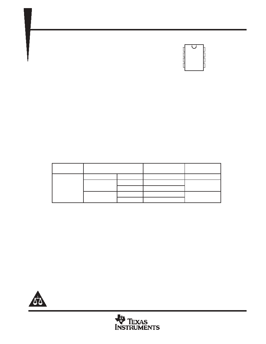
ORDERING INFORMATION
TA
PACKAGE
ORDERABLE
PART NUMBER
TOP-SIDE
MARKING
PDIP (P)
Tube of 50
RC4580IP
RC4580IP
SOIC (D)
Tube of 75
RC4580ID
R4580I
-40
∞
C to 85
∞
C
SOIC (D)
Reel of 2500
RC4580IDR
R4580I
-40 C to 85 C
TSSOP (PW)
Tube of 150
RC4580IPW
R4580I
TSSOP (PW)
Reel of 2000
RC4580IPWR
R4580I
Package drawings, standard packing quantities, thermal data, symbolization, and PCB design guidelines are
available at www.ti.com/sc/package.
Please be aware that an important notice concerning availability, standard warranty, and use in critical applications of
Texas Instruments semiconductor products and disclaimers thereto appears at the end of this data sheet.
Copyright
2004, Texas Instruments Incorporated
1
2
3
4
8
7
6
5
1OUT
1IN-
1IN+
V
CC-
V
CC+
2OUT
2IN-
2IN+
D, P, OR PW PACKAGE
(TOP VIEW)
PRODUCTION DATA information is current as of publication date.
Products conform to specifications per the terms of Texas Instruments
standard warranty. Production processing does not necessarily include
testing of all parameters.

RC4580
DUAL AUDIO OPERATIONAL AMPLIFIER
SLOS412C - APRIL 2003 - REVISED MARCH 2004
2
POST OFFICE BOX 655303
∑
DALLAS, TEXAS 75265
equivalent schematic
Output
VCC+
- Input
+ Input
VCC-
RC4580
DUAL AUDIO OPERATIONAL AMPLIFIER
SLOS412C - APRIL 2003 - REVISED MARCH 2004
3
POST OFFICE BOX 655303
∑
DALLAS, TEXAS 75265
absolute maximum ratings over operating free-air temperature range (unless otherwise noted)
Supply voltage, V
CC+
±
18 V
. . . . . . . . . . . . . . . . . . . . . . . . . . . . . . . . . . . . . . . . . . . . . . . . . . . . . . . . . . . . . . . . . . . . .
Input voltage (any input)
±
15 V
. . . . . . . . . . . . . . . . . . . . . . . . . . . . . . . . . . . . . . . . . . . . . . . . . . . . . . . . . . . . . . . . . . .
Differential input voltage, V
ID
±
30 V
. . . . . . . . . . . . . . . . . . . . . . . . . . . . . . . . . . . . . . . . . . . . . . . . . . . . . . . . . . . . . . .
Output current
±
50 mA
. . . . . . . . . . . . . . . . . . . . . . . . . . . . . . . . . . . . . . . . . . . . . . . . . . . . . . . . . . . . . . . . . . . . . . . . . .
Package thermal impedance,
JA
(see Notes 1 and 2): D package
97
∞
C/W
. . . . . . . . . . . . . . . . . . . . . . . . . . . .
P package
85
∞
C/W
. . . . . . . . . . . . . . . . . . . . . . . . . . . . .
PW package
149
∞
C/W
. . . . . . . . . . . . . . . . . . . . . . . . . .
Operating virtual junction temperature, T
J
150
∞
C
. . . . . . . . . . . . . . . . . . . . . . . . . . . . . . . . . . . . . . . . . . . . . . . . . . .
Storage temperature range, T
stg
-60
∞
C to 125
∞
C
. . . . . . . . . . . . . . . . . . . . . . . . . . . . . . . . . . . . . . . . . . . . . . . . . . .
Stresses beyond those listed under "absolute maximum ratings" may cause permanent damage to the device. These are stress ratings only, and
functional operation of the device at these or any other conditions beyond those indicated under "recommended operating conditions" is not
implied. Exposure to absolute-maximum-rated conditions for extended periods may affect device reliability.
NOTES:
1. Maximum power dissipation is a function of TJ(max),
JA, and TA. The maximum allowable power dissipation at any allowable
ambient temperature is PD = (TJ(max) - TA)/
JA. Operating at the absolute maximum TJ of 150
∞
C can affect reliability.
2. The package thermal impedance is calculated in accordance with JESD 51-7.
recommended operating conditions
MIN
MAX
UNIT
VCC+
Supply voltage
2
16
V
VCC-
Supply voltage
-2
-16
V
VICR
Input common-mode voltage range
-13.5
13.5
V
TA
Operating free-air temperature range
-40
85
∞
C
electrical characteristics, V
CC
±
=
±
15 V, T
A
= 25
∞
C (unless otherwise noted)
PARAMETER
TEST CONDITIONS
MIN
TYP
MAX
UNIT
VIO
Input offset voltage
RS
10 k
0.5
3
mV
IIO
Input offset current
5
200
nA
IIB
Input bias current
100
500
nA
AVD
Large-signal differential-voltage amplification
RL
2 k
, VO =
±
10 V
90
110
dB
VOM
Output voltage swing
RL
2 k
±
12
±
13.5
V
VICR
Common-mode input voltage range
±
12
±
13.5
V
CMRR
Common-mode rejection ratio
RS
10 k
80
110
dB
kSVR
Supply-voltage rejection ratio
RS
10 k
80
110
dB
ICC
Supply current (all amplifiers)
6
9
mA
Measured with VCC
±
varied simultaneously
operating characteristics, V
CC
±
=
±
15 V, T
A
= 25
∞
C (unless otherwise noted)
PARAMETER
TEST CONDITIONS
TYP
UNIT
SR
Slew rate at unity gain
RL
2 k
5
V/
µ
s
GBW
Gain-bandwidth product
f = 10 kHz
12
MHz
THD
Total harmonic distortion
VO = 5 V, RL = 2 k
, f = 1 kHz, AVD = 20 dB
0.0005%
Vn
Equivalent input noise voltage
RIAA, RS
2.2 k
, 30-kHz LPF
0.8
µ
Vrms

RC4580
DUAL AUDIO OPERATIONAL AMPLIFIER
SLOS412C - APRIL 2003 - REVISED MARCH 2004
4
POST OFFICE BOX 655303
∑
DALLAS, TEXAS 75265
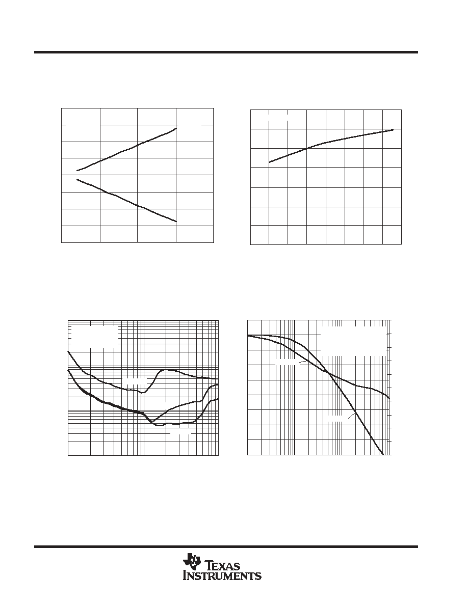
TYPICAL CHARACTERISTICS
Figure 1
-15
-10
-5
0
5
10
15
100
1 k
10 k
Maximum Output V
oltage Swing - V
RL - Load Resistance -
MAXIMUM OUTPUT VOLTAGE SWING
vs
LOAD RESISTANCE
VCC
±
=
±
15 V
TA = 25
∞
C
VOM+
VOM-
Figure 2
MAXIMUM OUTPUT VOLTAGE SWING
vs
FREQUENCY
0
5
10
15
20
25
30
1
5
10
50 60 70 80 100 200 300 500 700 1M 10M
Frequency - kHz
Maximum Output V
oltage Swing - V
V+/V- =
±
15 V
RL = 2 k
TA = 25
∞
C
Figure 3
OUTPUT VOLTAGE SWING
vs
OUTPUT CURRENT
Output V
oltage Swing - V
IO - Output Current - mA
VOM+
VOM-
VCC
±
=
±
15 V
20
15
10
5
0
-5
-10
-15
-20
1000
100
10
1
V - Equivalent Input Noise V
oltage -
0
10
20
30
10
100
1 k
10 k
100 k
Frequency - Hz
n
Figure 4
EQUIVALENT INPUT NOISE VOLTAGE
vs
FREQUENCY
VCC
±
=
±
1.5 V
RS = 50
AV = 60 dB
TA = 25
∞
C
nV/
Hz

RC4580
DUAL AUDIO OPERATIONAL AMPLIFIER
SLOS412C - APRIL 2003 - REVISED MARCH 2004
5
POST OFFICE BOX 655303
∑
DALLAS, TEXAS 75265
TYPICAL CHARACTERISTICS
0
2
4
6
8
10
12
14
16
18
-55
-40
0
25
70
85
125
Operating Current - mA
TA - Ambient Temperature -
∞
C
I - CC
Figure 5
OPERATING CURRENT
vs
TEMPERATURE
VCC
±
=
±
15 V
-15
-10
-5
0
5
10
15
-55
-40
0
25
70
85
105
TA - Ambient Temperature -
∞
C
V
O
VCC
±
= 15 V
RL = 2 k
- Output V
oltage Swing - V
Figure 6
OUTPUT VOLTAGE SWING
vs
TEMPERATURE
VOM+
VOM-
-100
-50
0
50
-50
-40
0
25
70
85
125
- Input Offset V
o
ltage - V
TA - Ambient Temperature -
∞
C
V
IO
µ
Figure 7
INPUT OFFSET VOLTAGE
vs
TEMPERATURE
100
VCC
±
=
±
15 V
TA - Ambient Temperature -
∞
C
0
100
200
300
400
-40
0
25
70
85
Input Bias Current - nA
VCC
±
=
±
15 V
I - IB
Figure 8
INPUT BIAS CURRENT
vs
TEMPERATURE
RC4580
DUAL AUDIO OPERATIONAL AMPLIFIER
SLOS412C - APRIL 2003 - REVISED MARCH 2004
6
POST OFFICE BOX 655303
∑
DALLAS, TEXAS 75265
TYPICAL CHARACTERISTICS
-20
-15
-10
-5
0
5
10
15
20
0
Maximum Output V
oltage Swing - V
V -
O
VCC+/VCC- - Operating Voltage - V
±
5
±
10
±
20
±
15
-VOM
TA = 25
∞
C
RL = 2 k
Figure 9
MAXIMUM OUTPUT VOLTAGE SWING
vs
OPERATING VOLTAGE
+VOM
0
1
2
3
4
5
6
7
Operating Current - mA
±
0
±
14
±
12
±
10
±
8
±
6
±
4
±
2
±
16
TA = 25
∞
C
VCC+/VCC- - Operating Voltage - V
Figure 10
OPERATING CURRENT
vs
OPERATING VOLTAGE
0.0001
0.001
0.01
0.1
0.1
1
10
THD - T
otal Harmonic Distortion - %
VO - Output Voltage - V
VCC
±
=
±
15 V
Gain = 20 dB
RL = 2 k
Figure 11
TOTAL HARMONIC DISTORTION
vs
OUTPUT VOLTAGE
20 Hz
1 kHz
20 kHz
0
5
10
15
20
25
30
35
40
45
10 k
100 k
1 M
10 M
-270
-240
-210
-180
-150
-120
-90
-60
-30
0
30
Phase - Deg
V
oltage Gain - dB
Frequency - Hz
VCC
±
=
±
15 V
RL = 2 k
40-dB Amplification
TA = 25
∞
C
Figure 12
VOLTAGE GAIN, PHASE
vs
FREQUENCY
Gain
Phase

MECHANICAL DATA
MPDI001A ≠ JANUARY 1995 ≠ REVISED JUNE 1999
POST OFFICE BOX 655303
∑
DALLAS, TEXAS 75265
P (R-PDIP-T8)
PLASTIC DUAL-IN-LINE
8
4
0.015 (0,38)
Gage Plane
0.325 (8,26)
0.300 (7,62)
0.010 (0,25) NOM
MAX
0.430 (10,92)
4040082/D 05/98
0.200 (5,08) MAX
0.125 (3,18) MIN
5
0.355 (9,02)
0.020 (0,51) MIN
0.070 (1,78) MAX
0.240 (6,10)
0.260 (6,60)
0.400 (10,60)
1
0.015 (0,38)
0.021 (0,53)
Seating Plane
M
0.010 (0,25)
0.100 (2,54)
NOTES: A. All linear dimensions are in inches (millimeters).
B. This drawing is subject to change without notice.
C. Falls within JEDEC MS-001
For the latest package information, go to http://www.ti.com/sc/docs/package/pkg_info.htm


MECHANICAL DATA
MTSS001C ≠ JANUARY 1995 ≠ REVISED FEBRUARY 1999
POST OFFICE BOX 655303
∑
DALLAS, TEXAS 75265
PW (R-PDSO-G**)
PLASTIC SMALL-OUTLINE PACKAGE
14 PINS SHOWN
0,65
M
0,10
0,10
0,25
0,50
0,75
0,15 NOM
Gage Plane
28
9,80
9,60
24
7,90
7,70
20
16
6,60
6,40
4040064/F 01/97
0,30
6,60
6,20
8
0,19
4,30
4,50
7
0,15
14
A
1
1,20 MAX
14
5,10
4,90
8
3,10
2,90
A MAX
A MIN
DIM
PINS **
0,05
4,90
5,10
Seating Plane
0
∞
≠ 8
∞
NOTES: A. All linear dimensions are in millimeters.
B. This drawing is subject to change without notice.
C. Body dimensions do not include mold flash or protrusion not to exceed 0,15.
D. Falls within JEDEC MO-153

IMPORTANT NOTICE
Texas Instruments Incorporated and its subsidiaries (TI) reserve the right to make corrections, modifications,
enhancements, improvements, and other changes to its products and services at any time and to discontinue
any product or service without notice. Customers should obtain the latest relevant information before placing
orders and should verify that such information is current and complete. All products are sold subject to TI's terms
and conditions of sale supplied at the time of order acknowledgment.
TI warrants performance of its hardware products to the specifications applicable at the time of sale in
accordance with TI's standard warranty. Testing and other quality control techniques are used to the extent TI
deems necessary to support this warranty. Except where mandated by government requirements, testing of all
parameters of each product is not necessarily performed.
TI assumes no liability for applications assistance or customer product design. Customers are responsible for
their products and applications using TI components. To minimize the risks associated with customer products
and applications, customers should provide adequate design and operating safeguards.
TI does not warrant or represent that any license, either express or implied, is granted under any TI patent right,
copyright, mask work right, or other TI intellectual property right relating to any combination, machine, or process
in which TI products or services are used. Information published by TI regarding third-party products or services
does not constitute a license from TI to use such products or services or a warranty or endorsement thereof.
Use of such information may require a license from a third party under the patents or other intellectual property
of the third party, or a license from TI under the patents or other intellectual property of TI.
Reproduction of information in TI data books or data sheets is permissible only if reproduction is without
alteration and is accompanied by all associated warranties, conditions, limitations, and notices. Reproduction
of this information with alteration is an unfair and deceptive business practice. TI is not responsible or liable for
such altered documentation.
Resale of TI products or services with statements different from or beyond the parameters stated by TI for that
product or service voids all express and any implied warranties for the associated TI product or service and
is an unfair and deceptive business practice. TI is not responsible or liable for any such statements.
Following are URLs where you can obtain information on other Texas Instruments products and application
solutions:
Products
Applications
Amplifiers
amplifier.ti.com
Audio
www.ti.com/audio
Data Converters
dataconverter.ti.com
Automotive
www.ti.com/automotive
DSP
dsp.ti.com
Broadband
www.ti.com/broadband
Interface
interface.ti.com
Digital Control
www.ti.com/digitalcontrol
Logic
logic.ti.com
Military
www.ti.com/military
Power Mgmt
power.ti.com
Optical Networking
www.ti.com/opticalnetwork
Microcontrollers
microcontroller.ti.com
Security
www.ti.com/security
Telephony
www.ti.com/telephony
Video & Imaging
www.ti.com/video
Wireless
www.ti.com/wireless
Mailing Address:
Texas Instruments
Post Office Box 655303 Dallas, Texas 75265
Copyright
2004, Texas Instruments Incorporated