
FEATURES
D
EXCELLENT SPECIFIED DRIFT
PERFORMANCE:
7ppm/
∞
C (max) at 0
∞
C to +125
∞
C
20ppm/
∞
C (max) at -40
∞
C to +125
∞
C
D
MICROSIZE PACKAGE: SOT23-6
D
HIGH OUTPUT CURRENT:
+
10mA
D
HIGH ACCURACY: 0.01%
D
LOW QUIESCENT CURRENT: 100
µ
A
D
LOW DROPOUT: 5mV
APPLICATIONS
D
PORTABLE EQUIPMENT
D
DATA ACQUISITION SYSTEMS
D
MEDICAL EQUIPMENT
D
TEST EQUIPMENT
1
GND_F
GND_S
3
2
ENABLE
5
6
4
OUT_S
IN
OUT_F
REF3212
REF3220
REF3225
REF3230
REF3233
REF3240
DESCRIPTION
The REF32xx is a very low drift, micropower, low-dropout,
precision voltage reference family available in the tiny
SOT23-6 package.
The small size and low power consumption (120
µ
A max)
of the REF32xx make it ideal for portable and
battery-powered applications. This reference is stable with
any capacitive load.
The REF32xx can be operated from a supply as low as
5mV above the output voltage, under no load conditions.
All models are specified for the wide temperature range of
-40
∞
C to +125
∞
C.
AVAILABLE OUTPUT VOLTAGES
PRODUCT
VOLTAGE
REF3212
1.25V
REF3220
2.048V
REF3225
2.5V
REF3230
3.0V
REF3233
3.3V
REF3240
4.096V
REF3212, REF3220
REF3225, REF3230
REF3233, REF3240
SBVS058 -JUNE 2005
4ppm/
∞
C, 100
µ
A, SOT23-6
SERIES VOLTAGE REFERENCE
PRODUCTION DATA information is current as of publication date. Products
conform to specifications per the terms of Texas Instruments standard warranty.
Production processing does not necessarily include testing of all parameters.
www.ti.com
Copyright
2005, Texas Instruments Incorporated
Please be aware that an important notice concerning availability, standard warranty, and use in critical applications of Texas Instruments
semiconductor products and disclaimers thereto appears at the end of this data sheet.
All trademarks are the property of their respective owners.

REF3212, REF3220
REF3225, REF3230
REF3233, REF3240
SBVS058 -JUNE 2005
www.ti.com
2
ABSOLUTE MAXIMUM RATINGS
(1)
Input Voltage
+7.5V
. . . . . . . . . . . . . . . . . . . . . . . . . . . . . . . . . . . . . . . . . . . . . .
Operating Temperature
-55
∞
C to +135
∞
C
. . . . . . . . . . . . . . . . . . . . . . . . . . . .
Storage Temperature
-65
∞
C to +150
∞
C
. . . . . . . . . . . . . . . . . . . . . . . . . . . . . .
Junction Temperature
+150
∞
C
. . . . . . . . . . . . . . . . . . . . . . . . . . . . . . . . . . . . .
Lead Temperature (soldering, 10s)
+300
∞
C
. . . . . . . . . . . . . . . . . . . . . . . . . . .
ESD Rating
Human Body Model
4kV
. . . . . . . . . . . . . . . . . . . . . . . . . . . . . . . . . . . . . . . . .
Charged Device Model
1kV
. . . . . . . . . . . . . . . . . . . . . . . . . . . . . . . . . . . . . .
Machine Model
400V
. . . . . . . . . . . . . . . . . . . . . . . . . . . . . . . . . . . . . . . . . . .
(1) Stresses above these ratings may cause permanent damage. Exposure
to absolute maximum conditions for extended periods may degrade
device reliability. These are stress ratings only, and functional operation of
the device at these or any other conditions beyond those specified is not
implied.
This integrated circuit can be damaged by ESD. Texas
Instruments recommends that all integrated circuits be
handled with appropriate precautions. Failure to observe
proper handling and installation procedures can cause damage.
ESD damage can range from subtle performance degradation to
complete device failure. Precision integrated circuits may be more
susceptible to damage because very small parametric changes could
cause the device not to meet its published specifications.
PACKAGE/ORDERING INFORMATION
(1)
PRODUCT
OUTPUT VOLTAGE
PACKAGE-LEAD
PACKAGE DESIGNATOR
PACKAGE MARKING
REF3212
1.25V
SOT23-6
DBV
R32A
REF3212
1.25V
SOT23-6
DBV
R32A
REF3220
2.048V
SOT23-6
DBV
R32B
REF3220
2.048V
SOT23-6
DBV
R32B
REF3225
2.5V
SOT23-6
DBV
R32C
REF3225
2.5V
SOT23-6
DBV
R32C
REF3230
3.0V
SOT23-6
DBV
R32D
REF3230
3.0V
SOT23-6
DBV
R32D
REF3233
3.30V
SOT23-6
DBV
R32E
REF3233
3.30V
SOT23-6
DBV
R32E
REF3240
4.096V
SOT23-6
DBV
R32F
REF3240
4.096V
SOT23-6
DBV
R32F
(1) For the most current package and ordering information, see the Package Option Addendum at the end of this document, or see the TI website at www.ti.com.
PIN CONFIGURATION
1
GND_F
GND_S
3
2
ENABLE
5
6
4
OUT_S
IN
OUT_F
R3
2x
Top View
SOT23
NOTE: The location of pin 1 on the REF32xx is determined by orienting the package marking as shown in the diagram above.
REF3212, REF3220
REF3225, REF3230
REF3233, REF3240
SBVS058 -JUNE 2005
www.ti.com
3
ELECTRICAL CHARACTERISTICS
Boldface limits apply over the listed temperature range.
At T
A
= +25
∞
C, I
LOAD
= 0mA, and V
IN
= 5V, unless otherwise noted.
REF32xx
PARAMETER
CONDITIONS
MIN
TYP
MAX
UNIT
REF3212 (1.25V)
OUTPUT VOLTAGE, V
OUT
1.2475
1.25
1.2525
V
Initial Accuracy
-0.2
0.01
0.2
%
NOISE
Output Voltage Noise
f = 0.1Hz to 10Hz
17
µ
V
PP
Voltage Noise
f = 10Hz to 10kHz
24
µ
V
RMS
REF3220 (2.048V)
OUTPUT VOLTAGE, V
OUT
2.044
2.048
2.052
V
Initial Accuracy
-0.2
0.01
0.2
%
NOISE
Output Voltage Noise
f = 0.1Hz to 10Hz
27
µ
V
PP
Voltage Noise
f = 10Hz to 10kHz
39
µ
V
RMS
REF3225 (2.5V)
OUTPUT VOLTAGE, V
OUT
2.495
2.50
2.505
V
Initial Accuracy
-0.2
0.01
0.2
%
NOISE
Output Voltage Noise
f = 0.1Hz to 10Hz
33
µ
V
PP
Voltage Noise
f = 10Hz to 10kHz
48
µ
V
RMS
REF3230 (3V)
OUTPUT VOLTAGE, V
OUT
2.994
3
3.006
V
Initial Accuracy
-0.2
0.01
0.2
%
NOISE
Output Voltage Noise
f = 0.1Hz to 10Hz
39
µ
V
PP
Voltage Noise
f = 10Hz to 10kHz
57
µ
V
RMS
REF3233 (3.3V)
OUTPUT VOLTAGE, V
OUT
3.293
3.3
3.307
V
Initial Accuracy
-0.2
0.01
0.2
%
NOISE
Output Voltage Noise
f = 0.1Hz to 10Hz
43
µ
V
PP
Voltage Noise
f = 10Hz to 10kHz
63
µ
V
RMS
REF3240 (4.096V)
OUTPUT VOLTAGE, V
OUT
4.088
4.096
4.104
V
Initial Accuracy
-0.2
0.01
0.2
%
NOISE
Output Voltage Noise
f = 0.1Hz to 10Hz
53
µ
V
PP
Voltage Noise
f = 10Hz to 10kHz
78
µ
V
RMS
REF3212, REF3220
REF3225, REF3230
REF3233, REF3240
SBVS058 -JUNE 2005
www.ti.com
4
ELECTRICAL CHARACTERISTICS (continued)
Boldface limits apply over the listed temperature range.
At T
A
= +25
∞
C, I
LOAD
= 0mA, and V
IN
= 5V, unless otherwise noted.
REF32xx
PARAMETER
UNIT
MAX
TYP
MIN
CONDITIONS
REF3212 / REF3220 / REF3225 / REF3230 / REF3233 / REF3240
OUTPUT VOLTAGE TEMP DRIFT
dV
OUT
/dT
0
∞
C
T
A
+125
∞
C
4
7
ppm/
∞
C
-40
∞
C
T
A
+125
∞
C
10.5
20
ppm/
∞
C
LONG-TERM STABILITY
0 to 1000h
55
ppm
LINE REGULATION
V
OUT
+ 0.05
(1)
V
IN
5.5V
-65
15
+65
ppm/V
LOAD REGULATION
dV
OUT
/dI
LOAD
Sourcing
0mA < I
LOAD
< 10mA, V
IN
= V
OUT
+ 250mV(1)
-40
3
40
µ
V/mA
Sinking
-10mA < I
LOAD
< 0mA, V
IN
= V
OUT
+ 100mV(1)
-60
20
60
µ
V/mA
THERMAL HYSTERESIS(2)
dT
First cycle
100
ppm
Additional cycles
25
ppm
DROPOUT VOLTAGE
(1)
VIN - VOUT
0
∞
C
T
A
+125
∞
C
5
50
mV
OUTPUT CURRENT
I
LOAD
V
IN
= V
OUT
+ 250mV
(1)
-10
10
mA
SHORT-CIRCUIT CURRENT
I
SC
Sourcing
50
mA
Sinking
40
mA
TURN-ON SETTLING TIME
to 0.1% at V
IN
= 5V with C
L
= 0
60
µ
s
ENABLE/SHUTDOWN
V
L
Reference in Shutdown mode
0
0.7
V
V
H
Reference is active
0.75
◊
V
IN
V
IN
V
POWER SUPPLY
I
L
= 0
Voltage
V
IN
V
OUT
+ 0.05
(1)
5.5
V
Current
I
Q
ENABLE > 0.75 x V
IN
100
120
µ
A
Over-temperature
0
∞
C
T
A
+125
∞
C
115
135
m
A
Shutdown
I
S
ENABLE < 0.7V
0.1
1
µ
A
TEMPERATURE RANGE
Specified
-40
+125
∞
C
Operating
-55
+135
∞
C
Storage
-65
+150
∞
C
Thermal resistance, SOT23-6
JA
200
∞
C/W
(1) The minimum supply voltage for the REF3212 is 1.8V.
(2) Thermal hysteresis procedure is explained in more detail in the Applications Information section.
(3) Load regulation is using force and sense lines; see the Load Regulation section for more information.
REF3212, REF3220
REF3225, REF3230
REF3233, REF3240
SBVS058 -JUNE 2005
www.ti.com
5
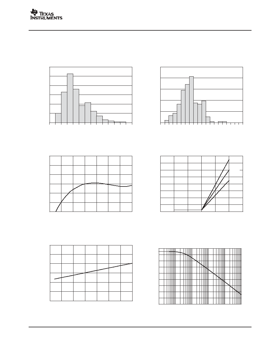
TYPICAL CHARACTERISTICS
At TA = +25
∞
C, I
LOAD
= 0mA, VIN = +5V power supply, REF3225 is used for typical characteristics, unless otherwise noted.
TEMPERATURE DRIFT
(0
_
C to +125
_
C)
Po
p
u
la
t
i
o
n
0.5
1.5
2.5
3.5
4.5
Drift (ppm/
_
C)
7
6.5
6
5
4
3
2
1
5.5
TEMPERATURE DRIFT
(
-
40
_
C to +125
_
C)
P
opul
ati
o
n
1 2 3 4 5 6 7 8 9
Drift (ppm/
_
C)
17 18 19 20
16
15
14
13
12
11
10
OUTPUT VOLTAGE ACCURACY
vs TEMPERATURE
0.12
0.08
0.04
0
-
0.04
-
0.08
-
0.12
O
u
tput
V
o
l
t
a
g
e
A
c
c
ur
ac
y
(
%
)
-
50
-
25
0
+25
+50
+75
+100
+125
Temperature (
_
C)
DROPOUT VOLTAGE
vs LOAD CURRENT
160
140
120
100
80
60
40
20
0
D
r
op
o
u
t
V
ol
t
a
g
e
(
m
V
)
-
15
15
10
5
0
-
5
-
10
Load Current (mA)
-
40
_
C
+25
_
C
+125
_
C
QUIESCENT CURRENT
vs TEMPERATURE
130
120
110
100
90
80
70
Q
u
ie
sce
n
t
C
u
rre
n
t
(
µ
A)
-
50
-
25
0
+25
+50
+75
+125
+100
Temperature (
_
C)
POWER-SUPPLY REJECTION RATIO
vs FREQUENCY
100
90
80
70
60
50
40
30
20
10
PS
R
R
(
d
B
)
1
10
100
1k
10k
100k
Frequency (Hz)