 | –≠–ª–µ–∫—Ç—Ä–æ–Ω–Ω—ã–π –∫–æ–º–ø–æ–Ω–µ–Ω—Ç: REG104FA | –°–∫–∞—á–∞—Ç—å:  PDF PDF  ZIP ZIP |

DMOS
1A Low-Dropout Regulator
FEATURES
q
NEW DMOS TOPOLOGY:
Ultra Low Dropout Voltage:
230mV typ at 1A and 3.3V Output
Output Capacitor NOT Required for Stability
q
FAST TRANSIENT RESPONSE
q
VERY LOW NOISE: 33
µ
V
RMS
q
HIGH ACCURACY:
±
2% max
q
HIGH EFFICIENCY:
I
GND
= 1.7mA at I
OUT
= 1A
Not Enabled: I
GND
= 0.5
µ
A
q
2.5V, 2.7V, 3.0V, 3.3V, 5.0V AND
ADJUSTABLE OUTPUT VERSIONS
q
THERMAL PROTECTION
q
SMALL SURFACE-MOUNT PACKAGES:
SOT223-5, DDPAK-5
APPLICATIONS
q
PORTABLE COMMUNICATION DEVICES
q
BATTERY-POWERED EQUIPMENT
q
MODEMS
q
BAR-CODE SCANNERS
q
BACKUP POWER SUPPLIES
DESCRIPTION
The REG104 is a family of low-noise, low-dropout linear
regulators with low ground pin current. Its new DMOS topol-
ogy provides significant improvement over previous designs,
including low dropout voltage (only 230mV typ at full load),
and better transient performance. In addition, no output
capacitor is required for stability, unlike conventional low
dropout regulators that are difficult to compensate and
require expensive low ESR capacitors greater than 1
µ
F.
Typical ground pin current is only 1.7mA (at I
OUT
= 1A) and
drops to 0.5
µ
A in
not enabled mode. Unlike regulators with
PNP pass devices, quiescent current remains relatively con-
stant over load variations and under dropout conditions.
The REG104 has very low output noise (typically 33
µ
V
RMS
for V
OUT
= 3.3V with C
NR
= 0.01
µ
F), making it ideal for use
in portable communications equipment. On-chip trimming
results in high output voltage accuracy. Accuracy is main-
tained over temperature, line, and load variations. Key pa-
rameters are tested over the specified temperature range
(≠40
∞
C to +85
∞
C).
The REG104 is well protected--internal circuitry provides a
current limit which protects the load from damage. Thermal
protection circuitry keeps the chip from being damaged by
excessive temperature. The REG104 is available in the
DDPAK-5 and the SOT223-5.
REG
104
REG104
REG104
(Fixed Voltage
Versions)
Enable
Gnd
0.1
µ
F
C
OUT
(1)
+
+
V
OUT
V
IN
NR
NR = Noise Reduction
NOTE: (1) Optional.
REG104-A
Gnd
Enable
0.1
µ
F
+
C
OUT
(1)
+
V
OUT
V
IN
R
2
R
1
Adj
REG104
SBVS025G ≠ SEPTEMBER 2001 ≠ REVISED SEPTEMBER 2005
www.ti.com
PRODUCTION DATA information is current as of publication date.
Products conform to specifications per the terms of Texas Instruments
standard warranty. Production processing does not necessarily include
testing of all parameters.
Copyright © 2001-2005, Texas Instruments Incorporated
Please be aware that an important notice concerning availability, standard warranty, and use in critical applications of
Texas Instruments semiconductor products and disclaimers thereto appears at the end of this data sheet.
All trademarks are the property of their respective owners.

SBVS025G
REG104
2
ABSOLUTE MAXIMUM RATINGS
(1)
Supply Input Voltage, V
IN
....................................................... ≠0.3V to 16V
Enable Input Voltage, V
EN
....................................................... ≠0.3V to V
IN
Feedback Voltage, V
FB
........................................................ ≠0.3V to 6.0V
NR Pin Voltage, V
NR
............................................................. ≠0.3V to 6.0V
Output Short-Circuit Duration ...................................................... Indefinite
Operating Temperature Range ....................................... ≠55
∞
C to +125
∞
C
Storage Temperature Range .......................................... ≠65
∞
C to +150
∞
C
Junction Temperature ..................................................... ≠55
∞
C to +150
∞
C
Lead Temperature (soldering, 3s, SOT, and DDPAK) ................... +240
∞
C
ESD Rating: HBM (V
OUT
to GND) ..................................................... 1.5kV
HBM (All other pins) ........................................................ 2kV
CDM .............................................................................. 500V
NOTE: (1) Stresses above these ratings may cause permanent damage.
Exposure to absolute maximum conditions for extended periods may degrade
device reliability.
PIN CONFIGURATIONS
Top View
NOTE: (1) For REG104A-A: voltage setting resistor pin.
All other models: noise reduction capacitor pin.
Gnd
Enable
V
IN
NR/Adjust
(1)
V
O
1 2 3 4 5
DDPAK-5
SOT223-5
(KTT Package)
(DCQ Package)
Tab is Gnd
Tab is Gnd
Enable
NR/Adjust
(1)
Gnd
V
IN
1
2
3
4
5
V
OUT
ELECTROSTATIC
DISCHARGE SENSITIVITY
This integrated circuit can be damaged by ESD. Texas Instru-
ments recommends that all integrated circuits be handled with
appropriate precautions. Failure to observe proper handling
and installation procedures can cause damage.
ESD damage can range from subtle performance degradation
to complete device failure. Precision integrated circuits may be
more susceptible to damage because very small parametric
changes could cause the device not to meet its published
specifications.
PACKAGE/ORDERING INFORMATION
(1)
PRODUCT
V
OUT
REG104xx-
yyyy/zzz
XX is package designator.
YYYY is typical output voltage (5 = 5.0V, 2.85 = 2.85V, A = Adjustable).
ZZZ is package quantity.
(1) For the most current package and ordering information, see the Package Option Addendum at the end of this document, or see the TI website at www.ti.com.

REG104
3
SBVS025G
REG104GA
REG104FA
PARAMETER
CONDITION
MIN
TYP
MAX
UNITS
OUTPUT VOLTAGE
Output Voltage Range
V
OUT
REG104-2.5
2.5
V
REG104-2.7
2.7
V
REG104-3.0
3.0
V
REG104-3.3
3.3
V
REG104-5
5
V
REG104-A
V
REF
5.5
V
Reference Voltage
V
REF
1.295
V
Adjust Pin Current
I
ADJ
0.2
1
µ
A
Accuracy
±
0.5
±
2
%
T
J
= ≠40
∞
C to +85
∞
C
±
3.0
%
vs Temperature
dV
OUT
/dT
T
J
= ≠40
∞
C to +85
∞
C
70
ppm/
∞
C
vs Line and Load
I
OUT
= 10mA to 1A, V
IN
= (V
OUT
+ 0.7V) to 15V
±
0.5
±
2.5
%
T
J
= ≠40
∞
C to +85
∞
C
V
IN
= (V
OUT
+ 0.9V) to 15V
±
3.5
%
DC DROPOUT VOLTAGE
(2, 3)
V
DROP
I
OUT
= 10mA
3
25
mV
For all models except 5V
I
OUT
= 1A
230
400
mV
For 5V model
I
OUT
= 1A 320
500
mV
For all models except 5V
I
OUT
= 1A
480
mV
T
J
= ≠40
∞
C to +85
∞
C
For 5V models
I
OUT
= 1A
580
mV
T
J
= ≠40
∞
C to +85
∞
C
VOLTAGE NOISE
f = 10Hz to 100kHz
V
n
Without C
NR
(all models)
C
NR
= 0, C
OUT
= 0
35
µ
V
RMS
/V ∑ V
OUT
µ
V
RMS
With C
NR
(all fixed voltage models)
C
NR
= 0.01
µ
F, C
OUT
= 10
µ
F
10
µ
V
RMS
/V ∑ V
OUT
µ
V
RMS
OUTPUT CURRENT
Current Limit
(4)
I
CL
1.2
1.7
2.1
A
T
J
= ≠40
∞
C to +85
∞
C
1.0
2.2
A
RIPPLE REJECTION
f = 120Hz
65
dB
ENABLE CONTROL
V
ENABLE
High (output enabled)
V
ENABLE
2
V
IN
V
V
ENABLE
Low (output disabled)
≠0.2
0.5
V
I
ENABLE
High (output enabled)
I
ENABLE
V
ENABLE
= 2V to V
IN
, V
IN
= 2.1V to 6.5
(5)
1
100
nA
I
ENABLE
Low (output disabled)
V
ENABLE
= 0V to 0.5V
2
100
nA
Output Disable Time
50
µ
s
Output Enable Softstart Time
1.5
ms
THERMAL SHUTDOWN
Junction Temperature
Shutdown
150
∞
C
Reset from Shutdown
130
∞
C
GROUND PIN CURRENT
Ground Pin Current
I
GND
I
OUT
= 10mA
0.5
0.7
mA
I
OUT
= 1A
1.7
1.8
mA
Enable Pin Low
V
ENABLE
0.5V
0.5
µ
A
INPUT VOLTAGE
V
IN
Operating Input Voltage Range
(6)
2.1
15
V
Specified Input Voltage Range
V
IN
> 2.7V
V
OUT
+ 0.7
15
V
T
J
= ≠40
∞
C to +85
∞
C
V
IN
> 2.9V
V
OUT
+ 0.9
15
V
TEMPERATURE RANGE
Specified Range
T
J
≠40
+85
∞
C
Operating Range
≠55
+125
∞
C
Storage Range
≠65
+150
∞
C
Thermal Resistance
DDPAK-5 Surface Mount
JC
Junction-to-Case
4
∞
C/W
SOT223-5 Surface Mount
JC
Junction-to-Case
15
∞
C/W
NOTES: (1) The REG104 does not require a minimum output capacitor for stability. However, transient response can be improved with proper capacitor selection.
(2) Dropout voltage is defined as the input voltage minus the output voltage that produces a 2% change in the output voltage from the value at V
IN
= V
OUT
+ 1V
at fixed load.
(3) Not applicable for V
OUT
less than 2.7V.
(4) Current limit is the output current that produces a 15% change in output voltage from V
IN
= V
OUT
+ 1V and I
OUT
= 10mA.
(5) For V
IN
> 6.5V, see typical characteristic
V
ENABLE
vs I
ENABLE
.
(6) The REG104 no longer regulates when V
IN
< V
OUT
+ V
DROP (MAX)
. In drop-out or when the input voltage is between 2.7V and 2.1V, the impedance from V
IN
to V
OUT
is typically less than 1
at T
J
= +25
∞
C. See typical characteristic
Output Voltage Change vs V
IN
.
ELECTRICAL CHARACTERISTICS
Boldface limits apply over the specified temperature range, T
J
= ≠40
∞
C to +85
∞
C
At T
J
= +25
∞
C, V
IN
= V
OUT
+ 1V (V
OUT
= 3.0V for REG104-A), V
ENABLE
= 2V, I
OUT
= 10mA, C
NR
= 0.01
µ
F, and C
OUT
= 0.1
µ
F
(1)
, unless otherwise noted.
SBVS025G
REG104
4
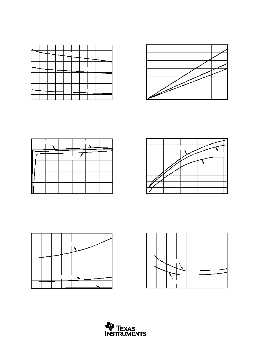
TYPICAL CHARACTERISTICS
For all models, at T
J
= +25
∞
C and V
ENABLE
= 2V, unless otherwise noted.
0
200
100
600
500
400
300
700
800 900 1000
0.8
0.6
0.4
0.2
0
≠0.2
≠0.4
≠0.6
≠0.8
≠1
≠1.2
Output Voltage Change (%)
Output Current (mA)
OUTPUT VOLTAGE CHANGE vs I
OUT
(V
IN
= V
OUT
+ 1V, Output Voltage % Change
Referred to I
OUT
= 10mA at +25
∞
C)
+125
∞
C
+25
∞
C
≠55
∞
C
0
200
600
400
800
1000
350
300
250
200
150
100
50
0
DC Dropout Voltage (mV)
I
OUT
(mA)
DC DROPOUT VOLTAGE vs I
OUT
+125
∞
C
+25
∞
C
≠55
∞
C
≠60
≠40
≠20
40
60
0
20
100
80
120
0.6
0.4
0.2
0
≠0.2
≠0.4
≠0.6
≠0.8
≠1
≠1.2
Output Voltage (%)
Temperature (
∞
C)
OUTPUT VOLTAGE CHANGE vs I
OUT
(Output Voltage % Change Referred to
I
OUT
= 10mA at +25
∞
C)
I
OUT
= 10mA
I
OUT
= 200mA
I
OUT
= 1000mA
≠75
≠50
≠25
25
50
0
100
75
125
350
300
250
200
150
100
50
0
DC Dropout Voltage (mV)
Temperature (
∞
C)
DC DROPOUT VOLTAGE vs TEMPERATURE
I
OUT
= 1000mA
I
OUT
= 200mA
I
OUT
= 10mA
≠75
≠50
≠25
25
50
0
100
75
125
0.5
0.4
0.3
0.2
0.1
0
Output Voltage Change (%)
Temperature (
∞
C)
LINE REGULATION vs TEMPERATURE
(V
IN
= V
OUT
+ 1V to 16V)
I
OUT
= 10mA
I
OUT
= 200mA
0
2
6
8
4
10
12
0.5
0
≠0.5
≠1
≠1.5
≠2
Output Voltage Change (%)
Input Voltage Above V
OUT
(V)
OUTPUT VOLTAGE CHANGE vs V
IN
(Output Voltage % Change Referred to
V
IN
= V
OUT
+ 1V at I
OUT
= 10mA)
I
OUT
= 10mA
I
OUT
= 1000mA
I
OUT
= 200mA
REG104
5
SBVS025G
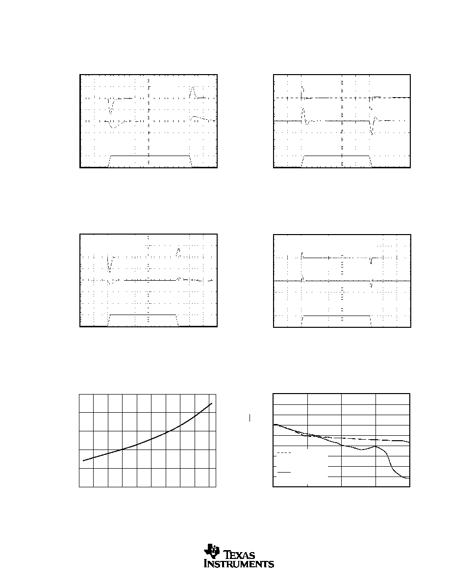
TYPICAL CHARACTERISTICS
(Cont.)
For all models, at T
J
= +25
∞
C and V
ENABLE
= 2V, unless otherwise noted.
6V
V
IN
V
OUT
V
OUT
5V
50mV/div
50mV/div
50
µ
s/div
LINE TRANSIENT RESPONSE
C
OUT
= 10
µ
F
C
OUT
= 0
REG104-3.3
I
OUT
= 200mA
1A
I
LOAD
V
OUT
V
OUT
10mA
500mV/div
500mV/div
10
µ
s/div
LOAD TRANSIENT RESPONSE
C
OUT
= 10
µ
F
C
OUT
= 0
REG104-3.3
C
OUT
= 0
REG104≠A
C
FB
= 0.01
µ
F, V
OUT
= 3.3V
C
OUT
= 10
µ
F
I
LOAD
1A
10mA
LOAD TRANSIENT RESPONSE
10
µ
s/div
500mV/div
500mV/div
C
OUT
= 0
REG104≠A
Load = 200mA, C
FB
= 0.01
µ
F, V
OUT
= 3.3V
C
OUT
= 10
µ
F
V
IN
6V
5V
LOAD TRANSIENT RESPONSE
50
µ
s/div
50mV/div
50mV/div
0.5
0.4
0.3
0.2
0.1
0
Output Voltage Change (%)
Temperature (
∞
C)
LOAD REGULATION vs TEMPERATURE
(V
IN
= V
OUT
+ 1V and 10mA < I
OUT
< 1000mA)
≠60
≠40
≠20
40
60
0
20
100
80
120
10
100
1000
10000
100,000
10
5
2
1
0.5
0.2
0.1
0.05
0.02
0.01
Noise Density (
µ
V/
Hz)
Frequency (Hz)
OUTPUT NOISE DENSITY
C
NR
= 0
C
OUT
= 0
C
NR
= 0.01
µ
F
C
OUT
= 10
µ
F