
1996
Application Specific Products
T
exas
I
nstruments
R
egistration
and
I
dentification
System
RI-RFM-006A
TIRIS RF-Module IC for Automotive
RI45538NS ( SOP package; Product Code: RI-RFM-006A-00 )
Reference Manual
and
Description of Application Circuit
REV 3.5

Rev. 3.5
RI-RFM-006A
TIRIS
RF-Module IC for Automotive
Page 1 of 19
IMPORTANT NOTICE
Texas Instruments (TI) reserves the right to make changes to its products or to discontinue any
product or service without notice, and advises its customers to obtain the latest version of relevant
information to verify, before placing orders, that the information being relied on is current.
TI warrants performance of its products and related software to the specifications applicable at
the time of sale in accordance with TI's standard warranty. Testing and other quality control
techniques are utilized to the extent TI deems necessary to support this warranty. Specific testing
of all parameters of each device is not necessarily performed, except those mandated by
government requirements.
Certain applications using products may involve potential risks of death, personal injury, or
severe property or environmental damage ("Critical Applications").
TI PRODUCTS ARE NOT DESIGNED, INTENDED, AUTHORIZED, OR WARRANTED
TO BE SUITABLE FOR USE IN LIFE-SUPPORT APPLICATIONS, DEVICES OR
SYSTEMS OR OTHER CRITICAL APPLICATIONS.
Inclusion of TI products in such applications is understood to be fully at the risk of the customer.
Use of TI products in such applications requires the written approval of an appropriate TI officer.
Questions concerning potential risk applications should be directed to TI through a local sales
office.
In order to minimize risks associated with the customer's applications, adequate design and
operating safeguards should be provided by the customer to minimize inherent or procedural
hazards.
TI assumes no liability for applications assistance, customer product design, software
performance, or infringement of patents or services described herein. Nor does TI warrant or
represent that any license, either express or implied, is granted under any patent right, copyright,
mask work right, or other intellectual property right of TI covering or relating to any combination,
machine, or process in which such products or services might be or are used.

Rev. 3.5
RI-RFM-006A
TIRIS
RF-Module IC for Automotive
Page 2 of 19
INDEX
IMPORTANT NOTICE
1
Overview
3
Features
3
TIRIS System Configuration (Schematic Diagram)
3
Internal Block Diagram and Pin Assignment
4
Description of Pins
5
Functions and Operation
6
1.
General
6
2.
Sending Mode
6
3.
Receiving Mode
7
Electrical Specifications
9
1.
Absolute Maximum Rating
9
2.
Recommended Operating Conditions
9
3.
Electrical Features under Recommended Operating Conditions
Input-Output Specifications
10
1.
Transmitter Signal I/O Timing
10
2.
Receiver Signal I/O Timing
10
Dimensional Outline Drawing - 16-pin SOP
12
Applied Circuit Configuration - Example
13
Typical Transmitter Circuit Configuration
14
Typical Receiver Circuit Configuration
15
Typical Antenna Circuit Configuration
16
Precautions for Mounting and Actual Use
17
1.
Power Supply Line
17
2.
Wiring for Antenna Circuit
18
Package
19
Rev. 3.5
RI-RFM-006A
TIRIS
RF-Module IC for Automotive
Page 3 of 19
!
Overview
RI-RFM-006A is a CMOS-technology based RF-module IC which integrates all transmitter-receiver
functions required for constructing a TIRIS Read-Write System into one single chip.
RI-RFM-006A consists of a transmitter signal control logic which generates signals for power
transmission and for sending the data you wrote to a remote TIRIS transponder, and a receiver which
amplifies and demodulates frequency shift keyed (FSK) signals received from this transponder.
Therefore, RI-RFM-006A is beneficially usable for constructing, in particular, a compact TIRIS Read-
Write System at a reduced cost. Furthermore, demodulation of the FSK signals received in its receiver
from a remote transponder is entirely digitized; this completely eliminates the need of regulations and
lessens the number of required external parts, thus enhancing the operational reliability of the system.
!
Features
The TIRIS RF-Module IC for Automotive Application, RI-RFM-006A, provides the following features
amongst others:
�
It incorporates a transmitter circuit with power selector and an open drain transmission power pre-
driver.
�
Also incorporated are a receiver signal amplifier and a digitized FSK signal demodulator.
�
I/O specifications: Conform to TIRIS standard RF-module specifications, with available signals of
TXCT-, RXDT-(*) and RXCK only.
(*) For RXDT- signals, this RF-module has a reverse polarity in relation to TIRIS standard
RF-modules. See the section "Description of Pins" for more information.
�
Operating supply voltage: 4.5 V to 5.5 V
�
Operating temperature range: -40
�
C to +85
�
C
�
Package: 16-pin SO package
�
Structure: CMOS process
!
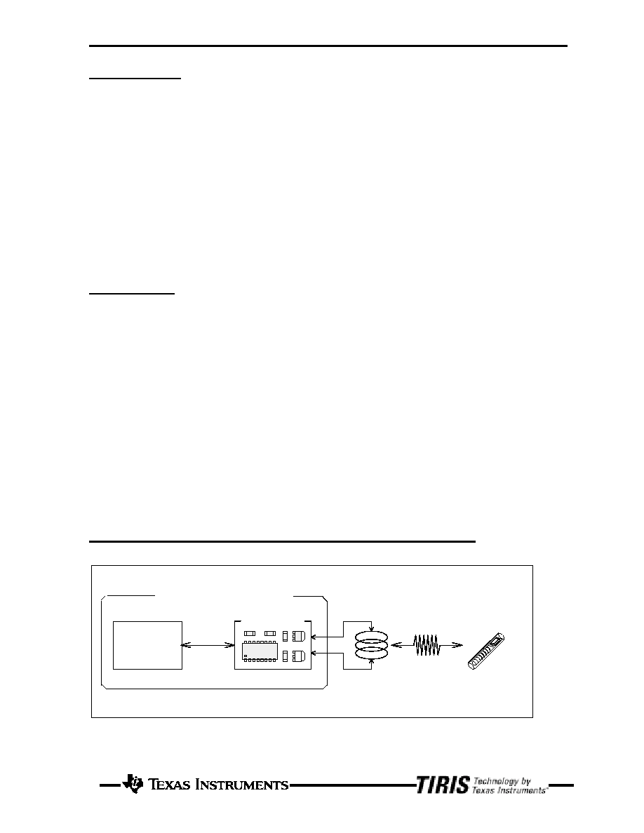
TIRIS System Configuration (Schematic Diagram)
TIRIS transponder
Controller
Serial
transmission
TIRIS RF-module
RI45538NS
TIRIS Read-Write System
Transmitter-receiver
Antenna
FSK
ASK
TIRIS System Configuration
Rev. 3.5
RI-RFM-006A
TIRIS
RF-Module IC for Automotive
Page 4 of 19
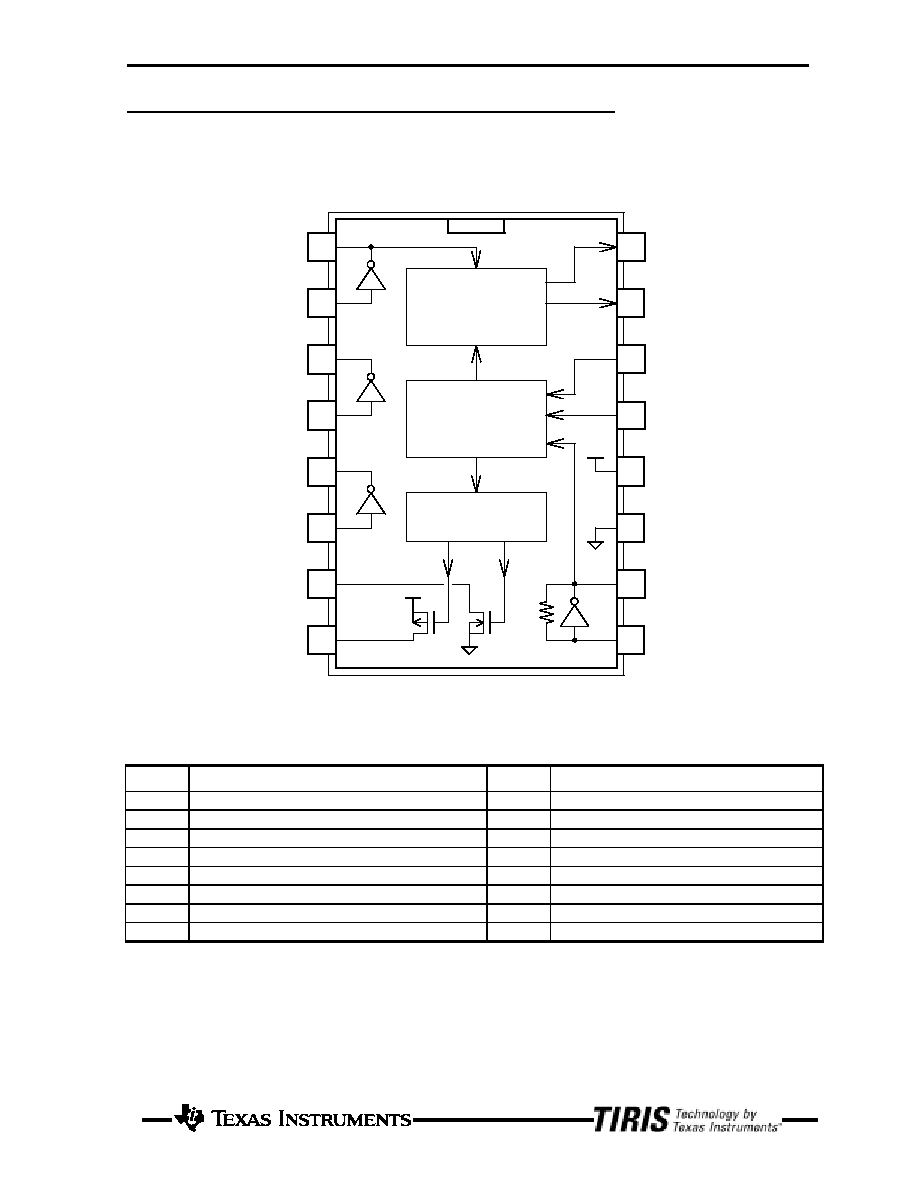
!
Internal Block Diagram and Pin Assignment
16
1
2
3
4
5
6
7
8
9
10
11
12
13
14
15
DIGITAL
DEMODULATOR
CONTROL
LOGIC
TRANSMITTER
NCH OPEN DRAIN
PCH OPEN DRAIN
MOS INVERTER
MOS INVERTER
MOS INVERTER
A3OP
A3IN
A2OP
A2IN
A1OP
A1IN
TXLO
TXHI
OSCI
OSCO
GND
VCC
TPC
TXCT-
RXDT-
RXCK
OSCILLATOR
Name
I/O Function
Name
I/O Function
A3OP
CMOS INVERTER-3/FSK SIGNAL OUTPUT
OSCI
OSCILLATOR INPUT(17.1776MHz typ.)
A3IN
CMOS INVERTER-3/FSK SIGNAL INPUT
OSCO
OSCILLATOR OUTPUT
A2OP
CMOS INVERTER-2 OUTPUT
GND
GND(POWER SUPPLY)
A2IN
CMOS INVERTER-2 INPUT
VCC
VCC(POWER SUPPLY)
A1OP
CMOS INVERTER-1 OUTPUT
TPC
TX-POWER Hi/Lo SELECT SIG. INPUT
A1IN
CMOS INVERTER-1 INPUT
TXCT-
TX-OUTPUT CONTROL SIGNAL INPUT
TXLO
TX-OUTPUT(NCH OPEN DRAIN OUTPUT)
RXDT-
RX-DATA("L"="1","H"="0") OUTPUT
TXHI
TX-OUTPUT(PCH OPEN DRAIN OUTPUT)
RXCK
RX-DATA CLOCK OUTPUT

Rev. 3.5
RI-RFM-006A
TIRIS
RF-Module IC for Automotive
Page 5 of 19
!
Description of Pins
Pin #
Signal
I/O
Description
1
A3OP
O
Signal output from CMOS inverter-3 amplifier; this pin is connected to the
internal FSK signal digital demodulator.
2
A3IN
I
Signal input to CMOS inverter-3 amplifier; if an external circuit is used to
amplify FSK signals, the amplified signals are input through this pin.
3
A2OP
O
Signal output from CMOS inverter-2 amplifier.
4
A2IN
I
Signal input to CMOS inverter-2 amplifier.
5
A1OP
O
Signal output from CMOS inverter-1 amplifier.
6
A1IN
I
I 16. Signal input to CMOS inverter-1 amplifier.
7
TXLO
Negative open
drain output
Negative level output of transmission signals; this output drives the
n-channel MOSFET used as antenna driver.
8
TXHI
Positive open
drain output
Positive level output of transmission signals; this output drives the
p-channel MOSFET used as antenna driver.
9
OSCI
I
Signal input to 17.1776 MHz master clock oscillator.
10
OSCO
O
Signal output from 17.1776 MHz master clock oscillator.
11
GND
-
Negative power supply.
12
VCC
-
Positive power supply.
13
TPC
I, w/pull-up
resistor
Input of transmission power selection signals (High-Low). A Low level
signal input through this pin substantially lowers the power during
transmission.
14
TXCT-
I, w/pull-up
resistor
Input of transmission output control signals (Transmit-Receive Mode
Selector). A Low level signal input through this pin outputs a transmission
signal to either "TXLO/TXHI" pin while a High level signal input turns the
mode to Receive and activates the internal FSK signal digital demodulator.
15
RXDT-
O
Serial output of demodulated FSK signal bit data. Negative level output
when the bit data received from the remote transponder is "1", and positive
level output when it is "0".
Note: The RI-RFM-006A has a reverse polarity in relation to TIRIS
standard RF-modules.
16
RXCK
O
Synchronous clock output of demodulated FSK signal data; a clock signal
synchronized with the "RXDT-" signal is output.
Rev. 3.5
RI-RFM-006A
TIRIS
RF-Module IC for Automotive
Page 6 of 19
!
Function and Operation
1. General
This RF-module IC counts on two operating modes:
Sending Mode - This mode is active when the "TXCT-" pin is set to L-level. A remote TIRIS
transponder can be charged up and ID code can be sent to that transponder in this mode.
Receiving Mode - This mode is active when the "TXCT-" pin is set to H-level. FSK signals sent from a
remote TIRIS transponder are received and demodulated in this mode.
Therefore, by switching over these modes using an external controller, data communications with a
TIRIS transponder can be made.
Note that this RF-module IC is exclusively designed to provide the user with a simple signal modulator-
demodulator (modem) function for data communications with a remote TIRIS transponder, based on the
appropriate data modulation-demodulation specifications. And therefore, it does not incorporate error
detection, data allotment nor other similar data processing functions in terms of protocol and data
formats.
(*) In both transmit and receive modes, this RF-module IC modulates and demodulates signals by logical
operation based on the incorporated master clock. This means that the modulating-demodulating
performance characteristics of this IC are directly affected by the frequency accuracy and variation of its
master clock (normal frequency is 17.1776 MHz). Therefore, the user is requested to select an oscillating
element or an external clock which is compatible with the remote TIRIS transponder to be used (see the
section describing the specifications "fexc", "fL" and "fH").
2. Sending Mode
In the Sending Mode, the frequency of the IC master clock (normal value: 17.1776 MHz) is divided
by 128. The resulting clock signal then has a frequency of 134.2 kHz (normal value). This resulting signal
is output as a composite signal for "TXHI" and "TXLO" terminals (pins) to drive the MOSFET which is
incorporated as an antenna resonance circuit driver, as illustrated below.
When the IC is in the Receiving Mode, its "TXHI" terminal is fixed at positive level and the "TXLO" at
high impedance. As a result, the output terminal "A" of the MOSFET used as an antenna resonance
circuit driver is fixed at negative level.
Note that when the IC is in the Sending Mode, its "RXDT-" terminal is always fixed at positive level and
as a consequence, the IC's FSK signal demodulator remains deactivated although data clock signals,
which are transmitted at a frequency resulting from division of the "A3IN" terminal signal frequency by
16, are output to the "RXCK".
7
8
RI45538NS
TXLO
TXHI
Master clock frequency divided by 128
(Ref. frequency, resulting: 134.2 kHz)
"A"
MOSFET(PCH)
MOSFET(NCH)
Rev. 3.5
RI-RFM-006A
TIRIS
RF-Module IC for Automotive
Page 7 of 19
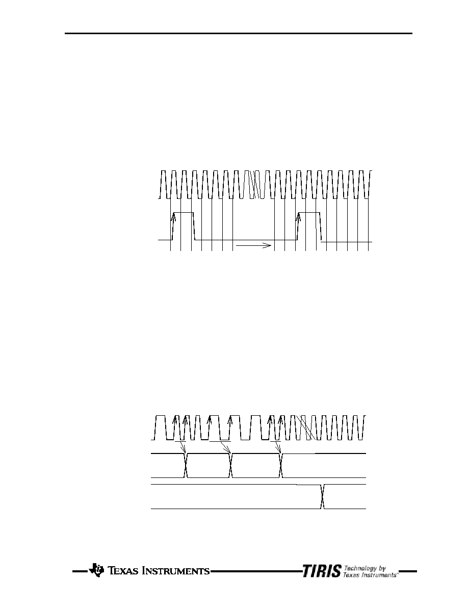
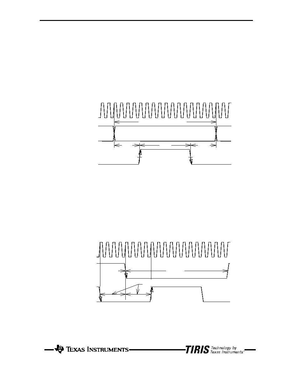
3.
Receiving Mode
In the Receiving Mode, the frequency-shift-keyed data signals are sequentially digitized to discriminate
their frequencies by binary notation (high-low) and demodulate them into bit strings consisting of bit data
"1" and "0".
For binary discrimination of signal frequencies between high and low, the frequency level of each
FS-keyed signal is measured from its leading edge at the "A3OP" terminal through to the next leading
edge by count of the internal master clock, as shown below. The threshold for this counted value
(x in the diagram below) is fixed at 132; when the clock count is over 132, it results in a negative level
output at the "RXDT-" terminal (bit data "1"), and when the clock count does not reach 132, a positive
level output at the same terminal (bit data "0"), respectively.
As the normal frequency of the internal master clock is 17.1776 MHz, one clock count is equivalent to
130.133... kHz (17.1776 MHz divided by 132 = 130.133... kHz). Accordingly, a signal is identified as bit
data "1" with the resulting negative level output at the "RXDT-" terminal when the signal frequency at
the "A3OP" terminal is 130.133... kHz or less, and it is identified as bit data "0" with the resulting
positive level output at the "RXDT-" terminal when the signal frequency at the "A3OP" terminal is over
130.133... kHz.
An additional feature is included to maximize the stability of the above-mentioned FSK signal
demodulating system based on binary notation: the system incorporates a circuit which disables definition
of an "RXDT-" signal unless more than four consecutive FS-keyed signal waves are identified within the
same frequency band during binary discrimination. This protects the once defined "RXDT-" signal in the
bit data form from being affected by sporadic events. For instance, even when its discrimination result is
sporadically inverted due to some noise effects, it is not affected if only three or less consecutive FS-
keyed signal waves are identified at the "A3OP" terminal. (See the diagram below.)
Note: For the timing between "A3OP" and "RXDT-" signals, refer to the section describing
"Input-Output Specifications".
The signals demodulated through the above-mentioned process are sequentially output from the "RXDT-"
Internal master clock
Signals discriminated
at A3OP terminal
Clock counts
1
1
2
3
4
5
6
X
X-1
2
3
4
5
6
7
Internal frequency
discriminating signals
Signal discriminated
at A3OP terminal
RXDT- terminal
output signals
DATA VALID
DATA VALID
Rev. 3.5
RI-RFM-006A
TIRIS
RF-Module IC for Automotive
Page 8 of 19
terminal in bit strings ("1" or "0"). To delimit these continuous bit strings, clock signals are output from
the "RXCK" terminal in synchronization with each bit data.
In normal operating conditions (when data communication can be properly performed between the RI-
RFM-006A and a TIRIS transponder), each bit data group sent from the remote transponder is composed
of sixteen consecutive signal waves belonging to the same frequency band (consisting of two wave
groups, 134.2-kHz high and 123.2-kHz low in terms of normal values). Therefore, clock signals at a
frequency resulting from a simple division of the "A3OP" terminal signal frequency by 16, are output
from the "RXCK" terminal. Then, each "RXCK" clock signal is controlled for output so that its first
transition falls after four consecutive "A3OP" signal waves from the "RXDT-" signal change point. This
enables an external controller to obtain the relevant bit data without fail provided that each "RXDT-"
signal is fetched well timed with the first transition of each "RXCK" signal. (See the diagram below.)
Sometimes at starting or during data receiving, some bit data group (composed of sixteen consecutive
signal waves belonging to the same frequency band) may be affected by interference noise, this causing
the number of its waves to vary and the consequent synchronous discrepancy between "RXDT-" and
"RXCK" signals. To correct this discrepancy, the sixteenth dividing counter of frequency incorporated in
this RF-module IC for "RXCK" clock signal generation are always reset at the moment at which any
internal demodulated bit data changes from "0" to "1" so that "RXCK" terminal signals are forcibly
output at L-level with the timing shown below. This correction is made automatically regardless of
whether or not receiving signals are properly input. (The frequency dividing counter is not reset at bit
data change from "1" to "0".)
Note: For details about timing among these signals, refer to the section describing "Input-
Output Specifications".
A3OP terminal signal
RXCK terminal output
DATA VALID
RXDT- terminal output
15
16
1
2
3
4
5
6
7
8
9
10
11
12
13
14
15
16
1
2
3
One bit data group (16 waves)
4 waves
4 waves
8 waves
A3OP terminal signal
RXCK terminal output
RXDT- terminal output
14
1
2
3
4
5
6
7
8
9
10
11
12
13
14
15
16
1
DATA="0"
16
DATA="1"
15
13
(each duration is equivalent to four A3OP terminal
Timing is controlled so that these durations are uniform

Rev. 3.5
RI-RFM-006A
TIRIS
RF-Module IC for Automotive
Page 9 of 19
!
Electrical Specifications
Absolute Maximum Rating
Supply voltage
(V
CC
)
- 0.5 to 7.0V
Input voltage range
(V
i
)
- 0.5 to 7.0V
Output voltage range
(V
o
)
- 0.5 to 7.0V
Input clamping current
(Iik)
� 20 mA
Output clamping current
(V
ok
)
� 20 mA
Output current
(I
out
(V
out
=0 to V
cc
))
� 25 mA
Operating temperature
(T
A
)
- 40 to +85�C
Storage temperature
(T
stg
)
- 65 to +150�C
Recommended Operating Conditions
Recommended Operating Conditions
MIN MAX
UNIT
Supply voltage, VCC
3.5 5.5
V
High-level input voltage, VIH
0.7Vcc
V
Low-level input voltage, VIL
0.2Vcc
V
Operating free-air temperature, TA
-40 85
�
C
Electrical Characteristics (VCC=5.0V, TA=25�C)
PARAMETER
CONDITIONS
MIN TYP MAX
UNIT
Vth Hysteresis voltage
1.7
V
IOH High-level output current
(TXHI)
(A2OP,A3OP)
(A1OP)
VOH=3.7V
6.8
20
73
144
mA
mA
uA
uA
IOL Low-level output current
(TXLO)
(A2OP,A3OP)
(A1OP)
VOL=0.5V
-6.8
-20
-72
-144
mA
mA
uA
uA
Ci Input capacitance
7.4
pF
Icc Supply current
35
mA
Note: Unless otherwise specified, all the voltage values indicated above are those measured
versus the "GND" pin of this RF-module IC.
Rev. 3.5
RI-RFM-006A
TIRIS
RF-Module IC for Automotive
Page 10 of 19
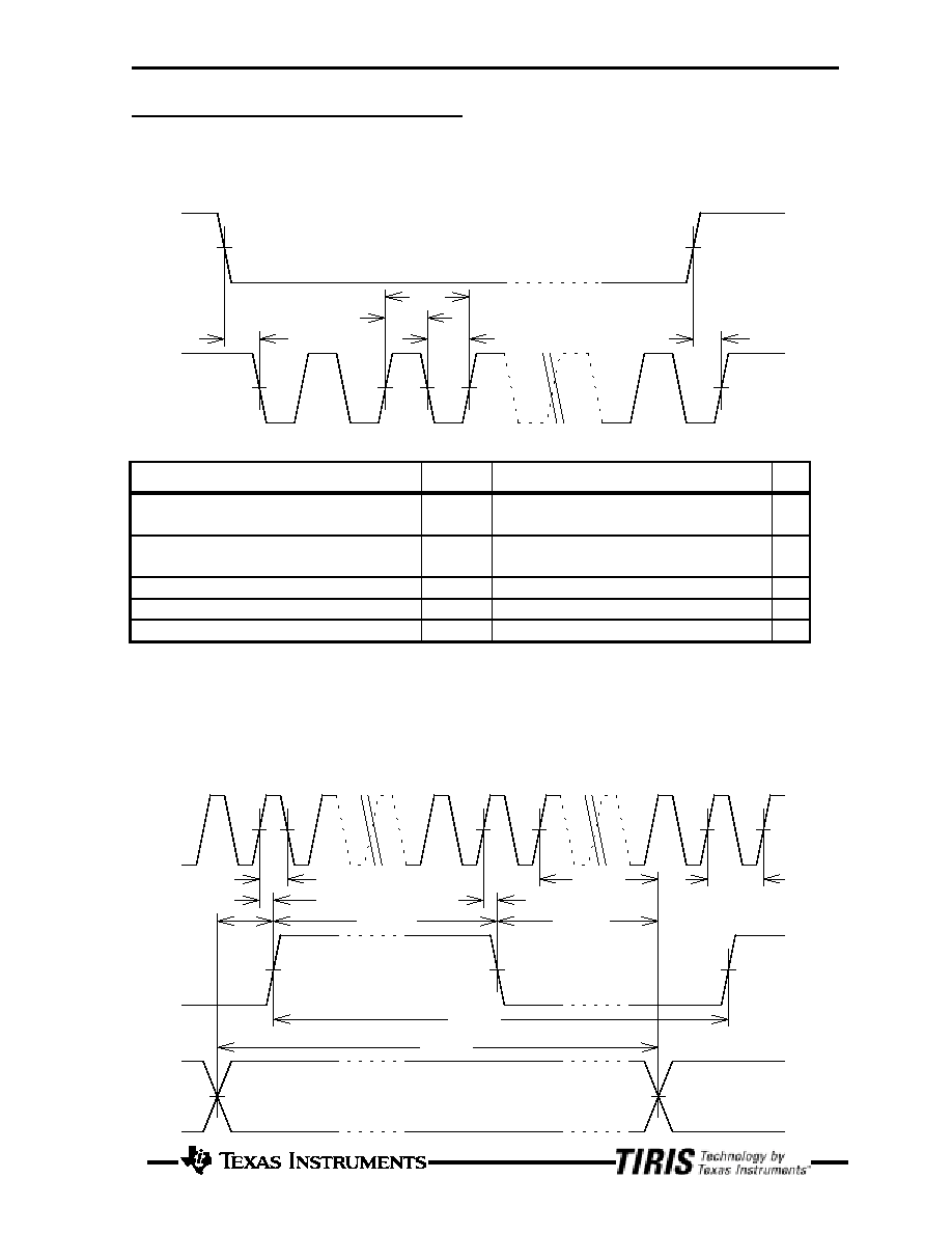
!
Input-Output Specifications
Transmitter Signal I/O Timing
TXCT-
TXHI+TXLO
tdl(TX)
tc(TX)
twh(TX)
twl(TX)
tdh(TX)
TX=
Item
Signal
Min. Typical Max.
Unit
Delay time between TXCT- and TX
trailing edges
t
dl
(TX)
64T
c
(OSC)
nS
Delay time between TXCT- and TX
leading edges
t
dh
(TX)
1T
c
(OSC)
nS
TX cycle time
t
c
(TX)
128T
c
(OSC)
nS
TX low level pulse duration
t
wl
(TX)
64T
c
(OSC)
nS
TX high level pulse duration
t
wh
(TX)
64T
c
(OSC)
nS
Note: "Tc
(osc)
" denotes the master clock cycle of this RF-module IC and its normal value is
specified at 56.3 ns (1/0.0171776). The same applies hereinafter. "TX" is defined as a
composite signal of "TXLO" and "TXHI" signals.
Receiver Signal I/O Timing
A3OP
RXCK
RXDT-
tdh(RXCK)
tdl(RXCK)
twh(RXCK)
tc(RXCK)
ts(RXDT)
tw(RXDT)
th(RXDT)
twh(A3OP)
DATA VALID
tc(A3OP)
td(RXDT)

Rev. 3.5
RI-RFM-006A
TIRIS
RF-Module IC for Automotive
Page 11 of 19
Item
Signal
Min. Typical Max.
Unit
A3OP cycle time for normal FSK signal
demodulation
t
c
(A3OP)
2T
c
(OSC)
nS
A3OP positive level pulse duration for normal
FSK signal demodulation
t
wh
(A3OP)
1T
c
(OSC)
nS
A3OP cycle time for negative level output of
RXDT- signal (bit data "1")
t
c
(A3OP)
132T
c
(OSC)
nS
Delay time between A3OP and RXCK leading
edges
t
dh
(RXCK)
1T
c
(OSC)
nS
Delay time between A3OP leading edge and
RXCK trailing edge
t
dl
(RXCK)
1T
c
(OSC)
nS
RXCK cycle time
t
c
(RXCK)
16T
c
(A3)
nS
RXCK positive level pulse duration
t
wh
(RXCK)
8T
c
(A3)
nS
Delay time from consecutive A3OP identical
signal waves to definition of an RXDT- signal
t
d
(RXDT)
16T
c
(A3)
+1T
c
(OSC)
nS
RXDT- positive/negative level duration, definite
t
w
(RXDT)
16T
c
(A3)
nS
RXDT- signal setup time in relation to RXCK
signal
t
s
(RXDT)
4T
c
(A3)
-1T
c
(OSC)
nS
RXDT-signal hold time in relation to RXCK
signal
t
h
(RXDT)
4T
c
(A3)
-1T
c
(OSC)
nS
Note: "Tc(A3)" denotes the signal cycle at the "A3OP" terminal and the above values are
based on the condition that a bit data group composed of sixteen consecutive signal waves
belonging to the same frequency band (sent from a remote TIRIS transponder in normal
operating conditions) has been previously input; otherwise, the values shown in the table
below shall apply.
Item
Signal
Min. Typical Max.
Unit
RXCK cycle time (except for normal signal
receiving)
t
c
(RXCK)
9T
c
(A3)
nS
RXCK positive level pulse duration (except for
normal signal receiving)
t
wh
(RXCK)
1T
c
(A3)
nS
RXDT- positive/negative level duration,
definite (except for normal signal receiving)
t
w
(RXDT)
9T
c
(A3)
nS
Rev. 3.5
RI-RFM-006A
TIRIS
RF-Module IC for Automotive
Page 12 of 19
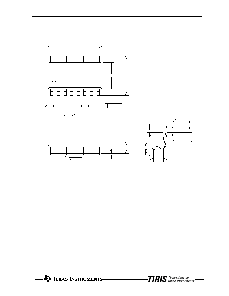
Dimensional Outline Drawing - 16-pin SOP
(Dimensions in mm)
9.90~10.50
0.81(MAX)
0.35~0.51
0.25
1.27(TYP)
5.00~5.60 7.40~8.20
0 - 10
0.55~1.05
2.00(MAX)
0.05(MIN)
0.10
�'P^�,�, ,
1
8
9
16
S57780 MA
YMLLLLJ
0.15(TYP)
RI45538NS
Rev. 3.5
RI-RFM-006A
TIRIS
RF-Module IC for Automotive
Page 13 of 19
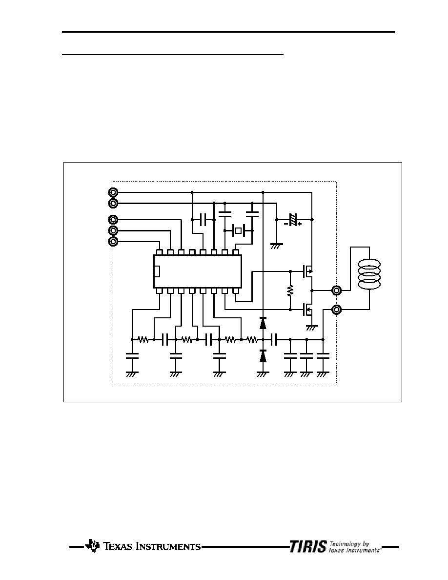
!
Applied Circuit Configuration - Example
Shown below is an example of applied circuit configuration for constructing a TIRIS Transmit-Receive
RF-module using the RI-RFM-006A. This example illustrates a simplified amplifier circuit for received
signals by eliminating a frequency band rejection filter which effectively eliminates external noises and
signals out of the frequency band of the response signals from the remote TIRIS transponder. In this
configuration, therefore, it is assumed that the available data communication distance of the system could
be easily affected by environmental conditions.
Note that this is only one of various possible applications. For more information of applied circuit
configurations, refer to the Application Handbook issued by our TIRIS Operation Dept.
* When configuring an applied circuit, take the following into account:
�
Choose the capacity of a resonance capacitor for clock generator oscillator in accordance with the
oscillator characteristics.
�
Define the frequency accuracy and variation of the clock generator oscillator by conversion based on
the specifications for the TIRIS transponder to be used together so that it can be within the range of
17.17248 MHz to 17.18272 MHz (standard frequency: 17.1776 MHz).
�
Select the values at resonance points around 134.2 kHz for L and C of the antenna circuit,
respectively. (In the example illustrated above, the following combination is used: antenna: 48
�
H;
capacitor: 0.03
�
F = 0.01
�
F x 3 units)
�
It is desirable to use a MOSFET having a low on-state resistance for antenna driver
TMS57780NS
9
10
11
12
13
14
15
16
5
1
2
3
4
6
7
8
ANTENNA
VCC
GND
TXCT
RXDT
RXCK
NC
1M
1200pF
68pF
68pF
68pF
0.01uF 0.01uF 0.01uF
120pF
120pF
1M
10K
100
1S1588
1S1588
120
100uF
0.1uF
17.1776MHz
(*)
(*)
2SJ182
2SK974
(L=48uH)
RI45538NS
Rev. 3.5
RI-RFM-006A
TIRIS
RF-Module IC for Automotive
Page 14 of 19
!
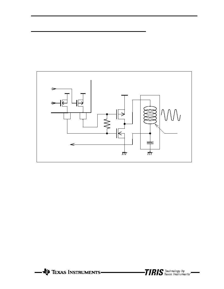
Typical Transmitter Circuit Configuration
This RF-module IC is provided with "TXHI" and "TXLO" terminals which can drive external MOSFETs
for driving the LC serial resonance antenna circuit. This resonance antenna circuit is to send 134.2-kHz
signals to the remote TIRIS transponder. Use these terminals as illustrated below.
In this circuit configuration, by selecting a value for R1 within a range of several hundred ohms and in
accordance with the characteristics of MOSFETs (T1 and T2) and introducing the selected value, the
through current which is consumed by the MOSFETs themselves during transmission can be reduced. If
the value for R1 is too high, the on-state resistances of T1 and T2 become very high and they will have
difficulty in driving the LC resonance circuit, leading to a possible reduction of available data
communication distance. Therefore, it is recommended that the value for R1 be defined after careful
evaluation of the characteristics of T1 and T2.
L1 and C1 in the LC resonance circuit may be mutually exchanged in position without giving significant
adverse effects to the operating performance of the circuit. However, the connection as is as illustrated
above is most preferable since it reduces potential influence of high-voltage transmission signals
produced at C1 on T1 and T2, thus a higher efficiency is gained.
RI45538NS
To receiving circuit
R1
7
TXLO
8
TXHI
LC resonance circuit
GND
VCC
134.2KHz
C1
L1
T1
T2
Antenna
Rev. 3.5
RI-RFM-006A
TIRIS
RF-Module IC for Automotive
Page 15 of 19
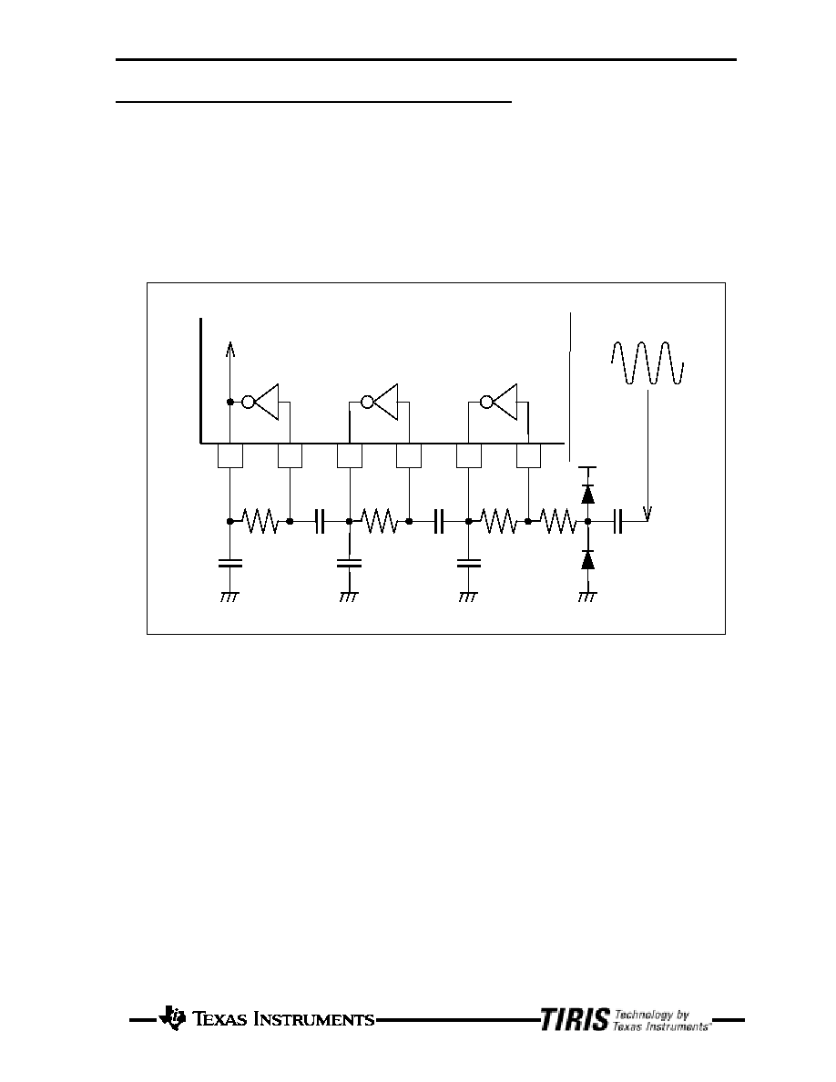
!
Typical Receiver Circuit Configuration
Three simple CMOS inverter type amplifiers are integrated in this RF-module IC in order to amplify the
FSK signals received from a remote TIRIS transponder up to a satisfactory logic level. The IC is
designed so as to permit their amplification factor and frequency characteristics to be selected within a
certain range by the use of appropriate external parts and/or circuits. A typical applied receiver circuit is
illustrated below.
In general, the FSK signals sent from a remote TIRIS transponder are found within a band of 120 kHz to
140 kHz, mainly due to dispersion of workmanship during manufacture and ambient temperature
fluctuation during transmitting operation. Therefore, by damping signals that fall out of the above band
range as much as possible, noise suppression performance can be improved. In the illustrated circuit
configuration, amplifier input coupling capacitors C2, C4 and C6 are used to reduce extremely
low-frequency noise signals, and amplifier output load capacitors C1, C3 and C5 to reduce
high-frequency noises. If you desire to enhance the noise resistance of the circuit still more, it is
necessary to install a required number of external wide band amplifiers with high amplification factor and
add an active band pass filter, LC resonance circuit, etc.
D1, D2 and R4 for input into the first amplifier (A1) form a circuit to prevent high-voltage signals for
power transmission and similar signals from entering the IC, thereby keeping from occurrence of
latch-up or other adverse situations. This circuit or otherwise, an equivalent protector, must be inserted
without fail.
1
2
3
4
5
6
To FSK signal demodulator
RI45538NS
R1
R2
R3
R4
C1
C2
C4
C5
A3OP
A3IN
A2OP
A2IN
A1OP
A1IN
From Antenna
C3
D2
D1
C6

Rev. 3.5
RI-RFM-006A
TIRIS
RF-Module IC for Automotive
Page 16 of 19
!
Typical Antenna Circuit Configuration
The antenna circuit consisting of L and C illustrated earlier in this manual (see the section describing
"Applied Circuit Configuration � Example") is designed to work as an LC serial resonance circuit in
which impedance drops in the presence of resonance frequencies during sending operation, and as an LC
parallel resonance circuit in which impedance increases in the presence of resonance frequencies during
receiving operation. The relationship between L and C incorporated in the resonance circuit can be
defined according to the following expression. Each value is calculated using this expression:
f
LC
(
)
134. 2KHz
=
1
2
The higher the Q value (quality factor) is, the higher transmission power the antenna L obtains and also
the higher the receiving gain becomes, thus allowing the system to have a greater available data
communication distance. If, however, at switch-over from power transmission mode to the receiving
mode, damping of the power transmission signal would not be completed before the remote TIRIS
transponder sends its ID code back to the IC, the signals sent from the transponder could not be received
properly. And the higher the Q value is, the longer the decay time of this power transmission signal will
be. It has been revealed by experimental testing that an antenna with its maximum Q value of around 30 is
usable in the circuit as is as illustrated in the "Applied Circuit Configuration � Example" section. If it is
desired to use an antenna having a higher Q value, some measures must be devised and added to this
circuit.
Additionally, the characteristics and efficiency of the resonance circuit used here greatly depend not only
on the antenna L but also on the capacitor C and the MOSFETs which drive them. Therefore, the
application of the lowest possible impedance at the frequency f(134.2 kHz) to them will permit a higher
transmission power, and as a result, it will allow the system to have a greater available data
communication distance with the remote transponder.
Rev. 3.5
RI-RFM-006A
TIRIS
RF-Module IC for Automotive
Page 17 of 19
!
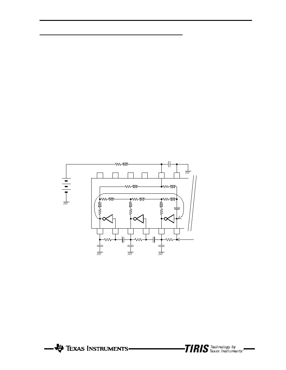
Precautions for Mounting and Actual Use
Described in this section are the precautions to be taken at mounting and actual use of the RI-RFM-006A
while designing and manufacturing a TIRIS Read-Write System using this IC, especially, critical issues
as may affect the operating performance of the IC and, in particular, the system communication
performance with a remote TIRIS transponder.
1. Power Supply Line
When the signals returned from a remote TIRIS transponder are amplified by sequentially using the three
CMOS inverter type amplifiers incorporated in this RF-module IC, an undesirable feedback loop is
formed from the third amplifier toward the first one through parasitic L, R and C whose formation is not
avoidable because of the structure of this IC and its internal power supply line (see the diagram below) as
CMOS devices are inevitably bi-directional. If this feedback loop is left as is, it normally leads to an
oscillation; particularly, when the frequency band of each amplifier is limited so that it matches that of
the transponder return signals, oscillation occurs at a frequency within this band which counts on high
gains from the very nature of things, in consequence, adversely affecting the demodulating performance
of the received FSK signals.
Equivalent circuit for internal power supply line feedback loop
This situation does not a little occur when a multiple number of high-gain amplifiers are integrated in a
CMOS device. Formation of this undesirable feedback loop in the amplifier band can be avoided by
minimizing the impedance of the power supply line through optimization of the printed circuit boards and
using a suitable bypass capacitor. It is extremely difficult to obtain true values for these parasitic L, R and
C forming the internal power supply line feedback loop, but it can be said from the empirical viewpoint
that it is possible to inhibit the said oscillation using a bypass capacitor with a capacity of
1
�
F and having a sufficiently low impedance within the said amplifier frequency band provided that
appropriate wiring patterns are defined for the power supply line on the printed circuit boards and in the
peripheries of external parts for the amplifiers.
Positive power supply (Vcc) line
Feedback loop
Bypass capacitor
From Antenna
1
2
3
4
5
6
16
15
14
13
12
11
Amplifier 1
Amplifier 2
Amplifier 3
Internal power supply line
Rev. 3.5
RI-RFM-006A
TIRIS
RF-Module IC for Automotive
Page 18 of 19
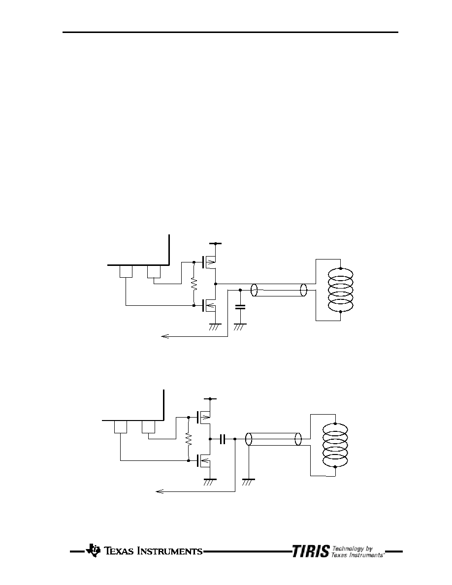
Wiring for Antenna Circuit
As previously described, the FSK signals sent from a remote TIRIS transponder are normally found
within a band of 120 kHz to 140 kHz. Therefore, the signal receiving circuit of this TIRIS Transmitter-
Receiver System is designed so that the signal amplification factor is necessarily highest within this band.
Because of this, all signals and noises which are produced by other devices and whose frequencies fall
within this band greatly affect the system performance, especially, its available data communication
distance with the remote TIRIS transponder among others.
In the same way, they have quite the undesirable effect not only upon the environment in which the
proper antenna for the system is found, but also upon the wire used to connect it with the IC's "A1IN" pin
which works as the first-phase amplifier for received signals. Furthermore, if there are wires for square or
pulse wave logic signals containing high-frequency components (even though their fundamental
frequencies are low) very close to this antenna connection wire, the system's available data
communication distance with the remote TIRIS transponder is further shortened due to the adverse
effects of such wires. For all that, if there is no other alternative than to use a long wiring between the IC
and its external antenna, it is suggested that a shielded wire be used for antenna wiring in either way as
illustrated below. With this, the antenna wiring will be less susceptible to the aforementioned adverse
effects.
a. When the antenna is driven first.
b. When the capacitor is driven first.
RI45538NS
7
8
TXLO
TXHI
To receiver amplifier
Shielded wire
Antenna
Antenna resonance capacitor
RI45538NS
7
8
TXLO
TXHI
To receiver amplifier
Shielded wire
Antenna
Antenna resonance capacitor
Rev. 3.5
RI-RFM-006A
TIRIS
RF-Module IC for Automotive
Page 19 of 19
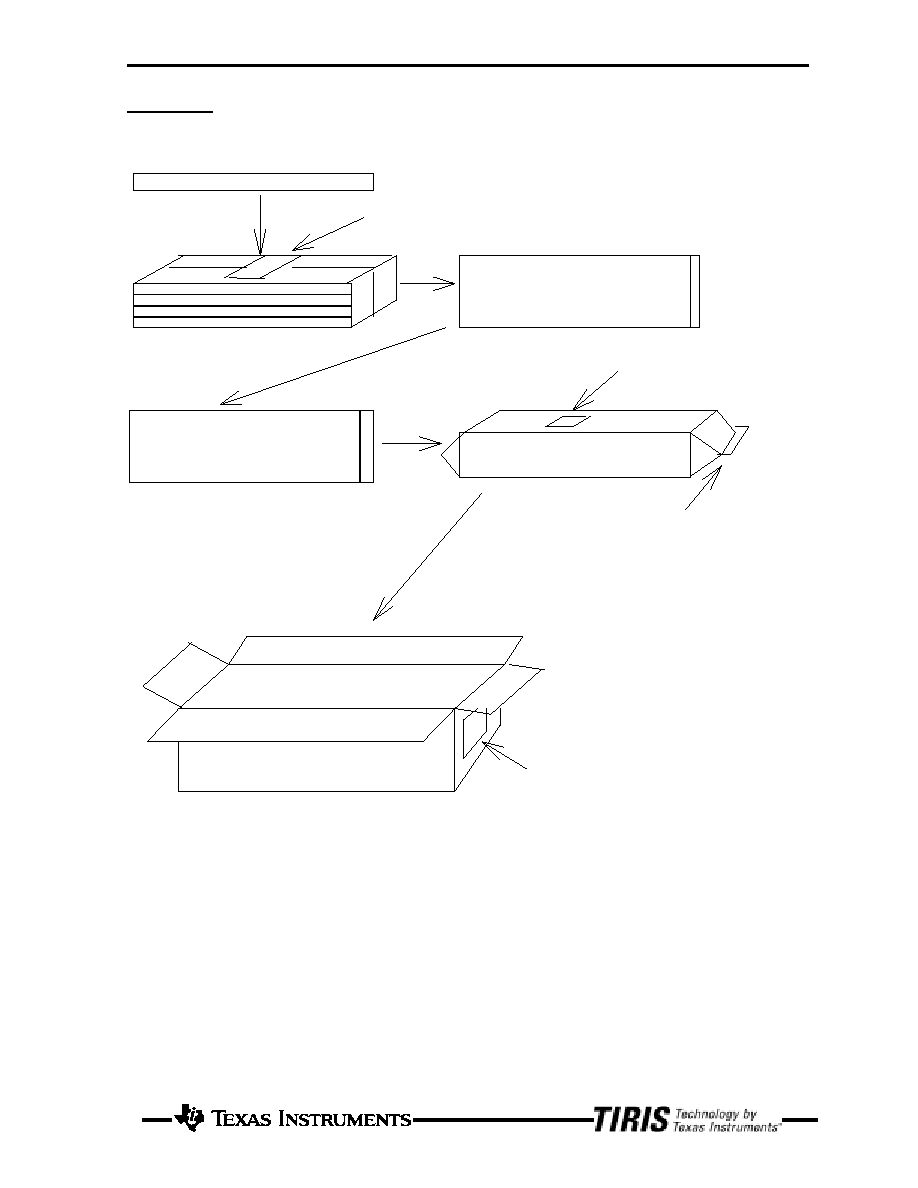
Package
Texas Instruments
50 pcs./tube
1,000 pcs. (20 tubes/bag)
Silica gel
Antistatic finish poly bag
Aluminum laminated case
Heat-sealed
Bar code label
Corrugated fiberboard case
Destination label