 | –≠–ª–µ–∫—Ç—Ä–æ–Ω–Ω—ã–π –∫–æ–º–ø–æ–Ω–µ–Ω—Ç: SA5534DR | –°–∫–∞—á–∞—Ç—å:  PDF PDF  ZIP ZIP |
NE5534, NE5534A, SA5534. SA5534A
LOW NOISE OPERATIONAL AMPLIFIERS
SLOS070C - JULY 1979 - REVISED SEPTEMBER 2004
1
POST OFFICE BOX 655303
∑
DALLAS, TEXAS 75265
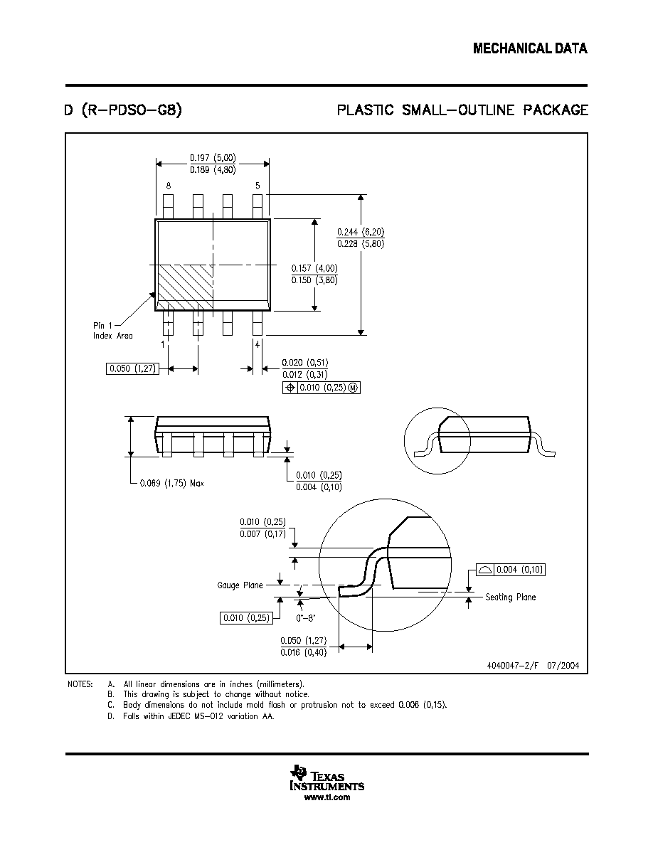
D
Equivalent Input Noise Voltage . . .
3.5 nV/
/
Hz Typ
D
Unity-Gain Bandwidth . . . 10 MHz Typ
D
Common-Mode Rejection Ratio . . .
100 dB Typ
D
High DC Voltage Gain . . . 100 V/mV Typ
D
Peak-to-Peak Output Voltage Swing
32 V Typ With V
CC
+
=
+
18 V and R
L
= 600
W
D
High Slew Rate . . . 13 V/
m
s Typ
D
Wide Supply-Voltage Range
+
3 V to
+
20 V
D
Low Harmonic Distortion
D
Offset Nulling Capability
D
External Compensation Capability
description/ordering information
The NE5534, NE5534A, SA5534, and SA5534A are high-performance operational amplifiers combining
excellent dc and ac characteristics. Some of the features include very low noise, high output-drive capability,
high unity-gain and maximum-output-swing bandwidths, low distortion, and high slew rate.
These operational amplifiers are compensated internally for a gain equal to or greater than three. Optimization
of the frequency response for various applications can be obtained by use of an external compensation
capacitor between COMP and COMP/BAL. The devices feature input-protection diodes, output short-circuit
protection, and offset-voltage nulling capability with use of the BALANCE and COMP/BAL pins (see the
application circuit diagram).
For the NE5534A and SA5534A, a maximum limit is specified for the equivalent input noise voltage.
Please be aware that an important notice concerning availability, standard warranty, and use in critical applications of
Texas Instruments semiconductor products and disclaimers thereto appears at the end of this data sheet.
Copyright
2004, Texas Instruments Incorporated
PRODUCTION DATA information is current as of publication date.
Products conform to specifications per the terms of Texas Instruments
standard warranty. Production processing does not necessarily include
testing of all parameters.
1
2
3
4
8
7
6
5
BALANCE
IN-
IN+
V
CC-
COMP/BAL
V
CC+
OUT
COMP
NE5534, SA5534 . . . D (SOIC), P (PDIP),
OR PS (SOP) PACKAGE
NE5534A, SA5534A . . . D (SOIC) OR P (PDIP) PACKAGE
(TOP VIEW)
NE5534, NE5534A, SA5534. SA5534A
LOW NOISE OPERATIONAL AMPLIFIERS
SLOS070C - JULY 1979 - REVISED SEPTEMBER 2004
2
POST OFFICE BOX 655303
∑
DALLAS, TEXAS 75265
description/ordering information (continued)
ORDERING INFORMATION
TA
VIOmax
AT 25
∞
C
PACKAGE
ORDERABLE
PART NUMBER
TOP-SIDE
MARKING
PDIP (P)
Tube of 50
NE5534P
NE5534P
PDIP (P)
Tube of 50
NE5534AP
NE5534AP
Tube of 75
NE5534D
NE5534
0
∞
C to 70
∞
C
4 mV
SOIC (D)
Reel of 2500
NE5534DR
NE5534
0 C to 70 C
4 mV
SOIC (D)
Tube of 75
NE5534AD
5534A
Reel of 2500
NE5534ADR
5534A
SOP (PS)
Reel of 2000
NE5534PSR
N5534
PDIP (P)
Tube of 50
SA5534P
SA5534P
PDIP (P)
Tube of 50
SA5534AP
SA5534AP
Tube of 75
SA5534D
SA5534
-40
∞
C to 85
∞
C
4 mV
SOIC (D)
Reel of 2500
SA5534DR
SA5534
-40
∞
C to 85
∞
C
4 mV
SOIC (D)
Tube of 75
SA5534AD
SA5534A
Reel of 2500
SA5534ADR
SA5534A
SOP (PS)
Tube of 80
SA553APS
SA5534
SOP (PS)
Reel of 2000
SA553APSR
SA5534
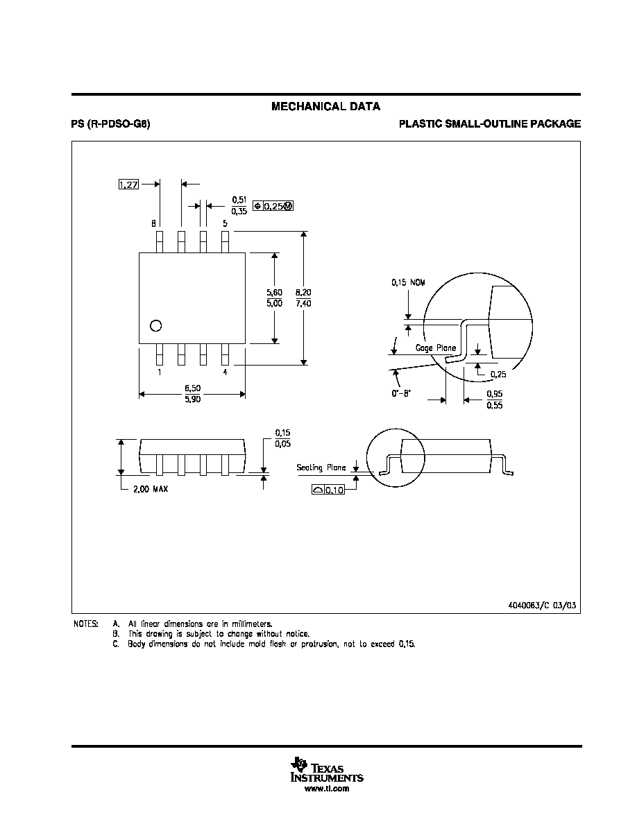
Package drawings, standard packing quantities, thermal data, symbolization, and PCB design guidelines are available
at www.ti.com/sc/package.
schematic
VCC-
OUT
15
15
12 k
12 k
7 pF
12 pF
40 pF
100 pF
IN+
IN-
BALANCE
COMP
COMP/BAL
8
5
7
4
6
2
3
1
All component values shown are nominal.
VCC+
NE5534, NE5534A, SA5534. SA5534A
LOW NOISE OPERATIONAL AMPLIFIERS
SLOS070C - JULY 1979 - REVISED SEPTEMBER 2004
3
POST OFFICE BOX 655303
∑
DALLAS, TEXAS 75265
symbol
IN-
COMP/BAL
COMP
OUT
BALANCE
-
+
IN+
application circuit
-
+
22 k
100 k
7
2
3
VCC-
4
6
5
8
VCC+
1
CC
5534
Frequency Compensation and Offset-Voltage Nulling Circuit
absolute maximum ratings over operating free-air temperature range (unless otherwise noted)
Supply voltage: V
CC+
(see Note 1)
22 V
. . . . . . . . . . . . . . . . . . . . . . . . . . . . . . . . . . . . . . . . . . . . . . . . . . . . . . . . . . .
V
CC-
(see Note 1)
-22 V
. . . . . . . . . . . . . . . . . . . . . . . . . . . . . . . . . . . . . . . . . . . . . . . . . . . . . . . . . .
Input voltage either input (see Notes 1 and 2)
V
CC+
. . . . . . . . . . . . . . . . . . . . . . . . . . . . . . . . . . . . . . . . . . . . . . . . .
Input current (see Note 3)
±
10 mA
. . . . . . . . . . . . . . . . . . . . . . . . . . . . . . . . . . . . . . . . . . . . . . . . . . . . . . . . . . . . . . . .
Duration of output short circuit (see Note 4)
Unlimited
. . . . . . . . . . . . . . . . . . . . . . . . . . . . . . . . . . . . . . . . . . . . . . .
Package thermal impedance,
JA
(see Notes 5 and 6): D package
97
∞
C/W
. . . . . . . . . . . . . . . . . . . . . . . . . . . .
P package
85
∞
C/W
. . . . . . . . . . . . . . . . . . . . . . . . . . . .
PS package
95
∞
C/W
. . . . . . . . . . . . . . . . . . . . . . . . . . .
Operating virtual junction temperature, T
J
150
∞
C
. . . . . . . . . . . . . . . . . . . . . . . . . . . . . . . . . . . . . . . . . . . . . . . . . . .
Storage temperature range, T
stg
-65
∞
C to 150
∞
C
. . . . . . . . . . . . . . . . . . . . . . . . . . . . . . . . . . . . . . . . . . . . . . . . . . .
Stresses beyond those listed under "absolute maximum ratings" may cause permanent damage to the device. These are stress ratings only, and
functional operation of the device at these or any other conditions beyond those indicated under "recommended operating conditions" is not
implied. Exposure to absolute-maximum-rated conditions for extended periods may affect device reliability.
NOTES:
1. All voltage values, except differential voltages, are with respect to the midpoint between VCC+ and VCC-.
2. The magnitude of the input voltage must never exceed the magnitude of the supply voltage.
3. Excessive current will flow if a differential input voltage in excess of approximately 0.6 V is applied between the inputs, unless some
limiting resistance is used.
4. The output may be shorted to ground or to either power supply. Temperature and/or supply voltages must be limited to ensure the
maximum dissipation rating is not exceeded.
5. Maximum power dissipation is a function of TJ(max),
JA, and TA. The maximum allowable power dissipation at any allowable
ambient temperature is PD = (TJ(max) - TA)/
JA. Operating at the absolute maximum TJ of 150
∞
C can affect reliability.
6. The package thermal impedance is calculated in accordance with JESD 51-7.
recommended operating conditions
MIN
MAX
UNIT
VCC+
Supply voltage
5
15
V
VCC-
Supply voltage
-5
-15
V
TA
Operating free-air temperature range
NE5534, NE5534A
0
70
∞
C
TA
Operating free-air temperature range
SA5534, SA5534A
-40
85
∞
C
NE5534, NE5534A, SA5534. SA5534A
LOW NOISE OPERATIONAL AMPLIFIERS
SLOS070C - JULY 1979 - REVISED SEPTEMBER 2004
4
POST OFFICE BOX 655303
∑
DALLAS, TEXAS 75265
electrical characteristics, V
CC
±
=
±
15 V, T
A
= 25
∞
C (unless otherwise noted)
PARAMETER
TEST CONDITIONS
MIN
TYP
MAX
UNIT
VIO
Input offset voltage
VO = 0,
TA = 25
∞
C
0.5
4
mV
VIO
Input offset voltage
VO = 0,
RS = 50
TA = Full range
5
mV
IIO
Input offset current
VO = 0
TA = 25
∞
C
20
300
nA
IIO
Input offset current
VO = 0
TA = Full range
400
nA
IIB
Input bias current
VO = 0
TA = 25
∞
C
500
1500
nA
IIB
Input bias current
VO = 0
TA = Full range
2000
nA
VICR
Common-mode input voltage range
±
12
±
13
V
VO(PP) Maximum peak-to-peak output voltage swing
RL
600
VCC
±
=
±
15 V
24
26
V
VO(PP) Maximum peak-to-peak output voltage swing
RL
600
VCC
±
=
±
18 V
30
32
V
AVD
Large-signal differential voltage amplification
VO =
±
10 V,
TA = 25
∞
C
25
100
V/mV
AVD
Large-signal differential voltage amplification
VO =
±
10 V,
RL
600
TA = Full range
15
V/mV
Avd
Small-signal differential voltage amplification
f = 10 kHz
CC = 0
6
V/mV
Avd
Small-signal differential voltage amplification
f = 10 kHz
CC = 22 pF
2.2
V/mV
VO =
±
10 V
CC = 0
200
BOM
Maximum-output-swing bandwidth
VO =
±
10 V
CC = 22 pF
95
kHz
BOM
Maximum-output-swing bandwidth
VCC
±
=
±
18 V,
RL
600
,
VO =
±
14 V,
CC = 22 pF
70
kHz
B1
Unity-gain bandwidth
CC = 22 pF,
CL = 100 pF
10
MHz
ri
Input resistance
30
100
k
zo
Output impedance
AVD = 30 dB,
CC = 22 pF,
RL
600
,
f = 10 kHz
0.3
CMRR
Common-mode rejection ratio
VO = 0,
RS = 50
VIC = VICRmin,
70
100
dB
kSVR
Supply-voltage rejection ratio (
VCC/
VIO)
VCC+ =
±
9 V to
±
15 V,
VO = 0
RS = 50
,
80
100
dB
IOS
Output short-circuit current
38
mA
ICC
Supply current
VO = 0, No load
TA = 25
∞
C
4
8
mA
All characteristics are measured under open-loop conditions with zero common-mode input voltage, unless otherwise specified.
For NE5534 and NE5534A, full range is 0
∞
C to 70
∞
C. For SA5534 and SA5534A, full range is -40
∞
C to 85
∞
C.
NE5534, NE5534A, SA5534. SA5534A
LOW NOISE OPERATIONAL AMPLIFIERS
SLOS070C - JULY 1979 - REVISED SEPTEMBER 2004
5
POST OFFICE BOX 655303
∑
DALLAS, TEXAS 75265
operating characteristics, V
CC
±
=
±
15 V, T
A
= 25
∞
C
PARAMETER
TEST CONDITIONS
NE5534,
SA5534
NE5534A, SA5534A
UNIT
PARAMETER
TEST CONDITIONS
TYP
MIN
TYP
MAX
UNIT
SR
Slew rate
CC = 0
13
13
V/ s
SR
Slew rate
CC = 22 pF
6
6
V/
µ
s
Rise time
VI = 50 mV,
RL = 600
,
AVD = 1,
CC = 22 pF
20
20
ns
tr
Overshoot factor
I
RL = 600
,
CL = 100 pF
CC = 22 pF
20
20
%
tr
Rise time
VI = 50 mV,
RL = 600
,
AVD = 1,
CC = 47 pF
50
50
ns
Overshoot factor
I
RL = 600
,
CL = 500 pF
CC = 47 pF
35
35
%
Vn
Equivalent input noise voltage
f = 30 Hz
7
5.5
7
nV/
Hz
Vn
Equivalent input noise voltage
f = 1 kHz
4
3.5
4.5
nV/
Hz
In
Equivalent input noise current
f = 30 Hz
2.5
1.5
pA/
Hz
In
Equivalent input noise current
f = 1 kHz
0.6
0.4
pA/
Hz
F
Average noise figure
RS = 5 k
,
f = 10 Hz to 20 kHz
0.9
dB
NE5534, NE5534A, SA5534. SA5534A
LOW NOISE OPERATIONAL AMPLIFIERS
SLOS070C - JULY 1979 - REVISED SEPTEMBER 2004
6
POST OFFICE BOX 655303
∑
DALLAS, TEXAS 75265
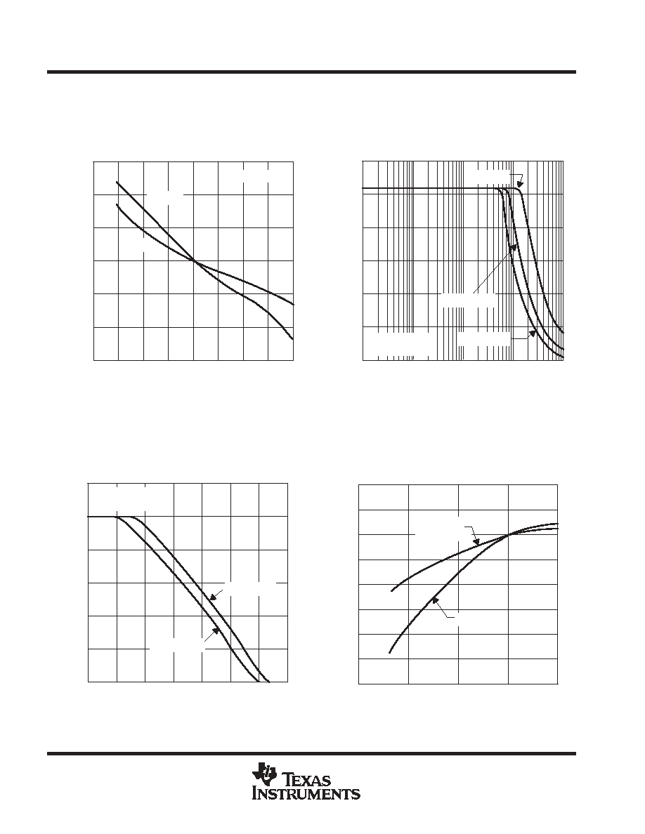
TYPICAL CHARACTERISTICS
Figure 1
1
0.8
0.6
0.4
-75 -50
-25
0
25
50
Normalized Input Bias Current and Input Offset Current
1.2
1.4
NORMALIZED INPUT BIAS CURRENT
AND INPUT OFFSET CURRENT
vs
FREE-AIR TEMPERATURE
1.6
75
100
125
TA - Free-Air Temperature -
∞
C
VCC
±
=
±
15 V
Offset
Bias
Figure 2
100
1 k
10 k
100 k
1 M
V
f - Frequency - Hz
MAXIMUM PEAK-TO-PEAK OUTPUT VOLTAGE
vs
FREQUENCY
OPP
- Maximum Peak-to-Peak Output V
o
ltage - V
30
25
20
15
10
5
0
¡¡
¡¡
¡¡
V
O(PP)
VCC
±
=
±
15 V
TA = 25
∞
C
CC = 22 pF
CC = 47 pF
CC = 0
Figure 3
A
LARGE-SIGNAL
DIFFERENTIAL VOLTAGE AMPLIFICATION
vs
FREQUENCY
f - Frequency - Hz
VCC
±
=
±
15 V
TA = 25
∞
C
CC = 0 pF
CC = 22 pF
106
105
104
103
102
10
1
VD
- Differential V
oltage
Amplification - V/mV
10
100
1 k
10 k
100 k
1 M
10 M 100 M
Figure 4
0.8
0.6
0.5
0.4
0
5
10
Normalized Slew Rate and Unity-Gain Bandwidth
1
1.1
NORMALIZED SLEW RATE AND
UNITY-GAIN BANDWIDTH
vs
SUPPLY VOLTAGE
1.2
15
20
0.9
0.7
| VCC
±
| - Supply Voltage - V
TA = 25
∞
C
Unity-Gain
Bandwidth
Slew Rate
Data at high and low temperatures are applicable only within the rated operating free-air temperature ranges of the various devices.
NE5534, NE5534A, SA5534. SA5534A
LOW NOISE OPERATIONAL AMPLIFIERS
SLOS070C - JULY 1979 - REVISED SEPTEMBER 2004
7
POST OFFICE BOX 655303
∑
DALLAS, TEXAS 75265
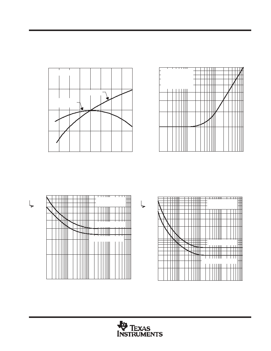
TYPICAL CHARACTERISTICS
Figure 5
1
0.9
0.8
-75
-50
-25
0
25
50
Normalized Slew Rate and Unity-Gain Bandwidth
1.1
NORMALIZED SLEW RATE AND
UNITY-GAIN BANDWIDTH
vs
FREE-AIR TEMPERATURE
1.2
75
100
125
VCC
±
=
±
15 V
TA - Free-Air Temperature -
∞
C
Unity-Gain
Bandwidth
Slew Rate
Figure 6
100
400
1 k
THD - T
otal Harmonic Distortion - %
f - Frequency - Hz
TOTAL HARMONIC DISTORTION
vs
FREQUENCY
4 k
10 k
40 k 100 k
0.01
0.007
0.004
0.002
0.001
VCC
±
=
±
15 V
AVD = 1
VI(rms) = 2 V
TA = 25
∞
C
Figure 7
10
100
- Equivalent Input Noise V
oltage -
f - Frequency - Hz
EQUIVALENT INPUT NOISE VOLTAGE
vs
FREQUENCY
1 k
10 k
100 k
V
n
nV/
Hz
10
7
4
2
1
VCC
±
=
±
15 V
TA = 25
∞
C
SA5534A, NE5534A
SA5534, NE5534
Figure 8
10
100
f - Frequency - Hz
1 k
10 k
100 k
EQUIVALENT INPUT NOISE CURRENT
vs
FREQUENCY
- Equivalent Input Noise Current -
I n
pA/
Hz
10
7
4
2
1
0.7
0.4
0.2
0.1
VCC
±
=
±
15 V
TA = 25
∞
C
SA5534, NE5534
SA5534A, NE5534A
Data at high and low temperatures are applicable only within the rated operating free-air temperature ranges of the various devices.
NE5534, NE5534A, SA5534. SA5534A
LOW NOISE OPERATIONAL AMPLIFIERS
SLOS070C - JULY 1979 - REVISED SEPTEMBER 2004
8
POST OFFICE BOX 655303
∑
DALLAS, TEXAS 75265
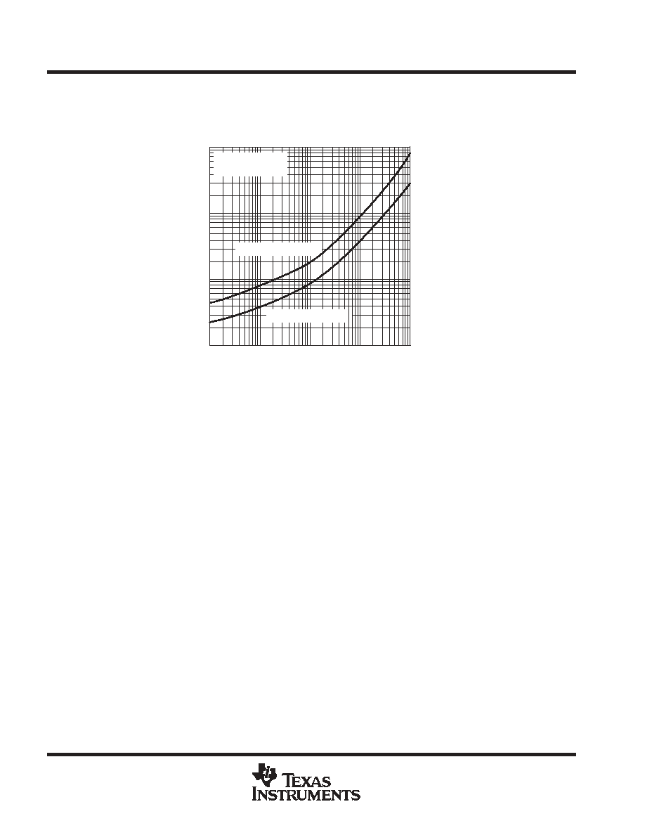
TYPICAL CHARACTERISTICS
Figure 9
0.7
0.4
0.2
0.1
100
1 k
10 k
100 k
1 M
T
otal Equivalent Input Noise V
oltage -
1
TOTAL EQUIVALENT INPUT NOISE VOLTAGE
vs
SOURCE RESISTANCE
7
4
2
10
70
40
20
100
µ
V
RS - Source Resistance -
VCC
±
=
±
15 V
TA = 25
∞
C
f = 10 Hz to 20 kHz
f = 200 Hz to 4 kHz
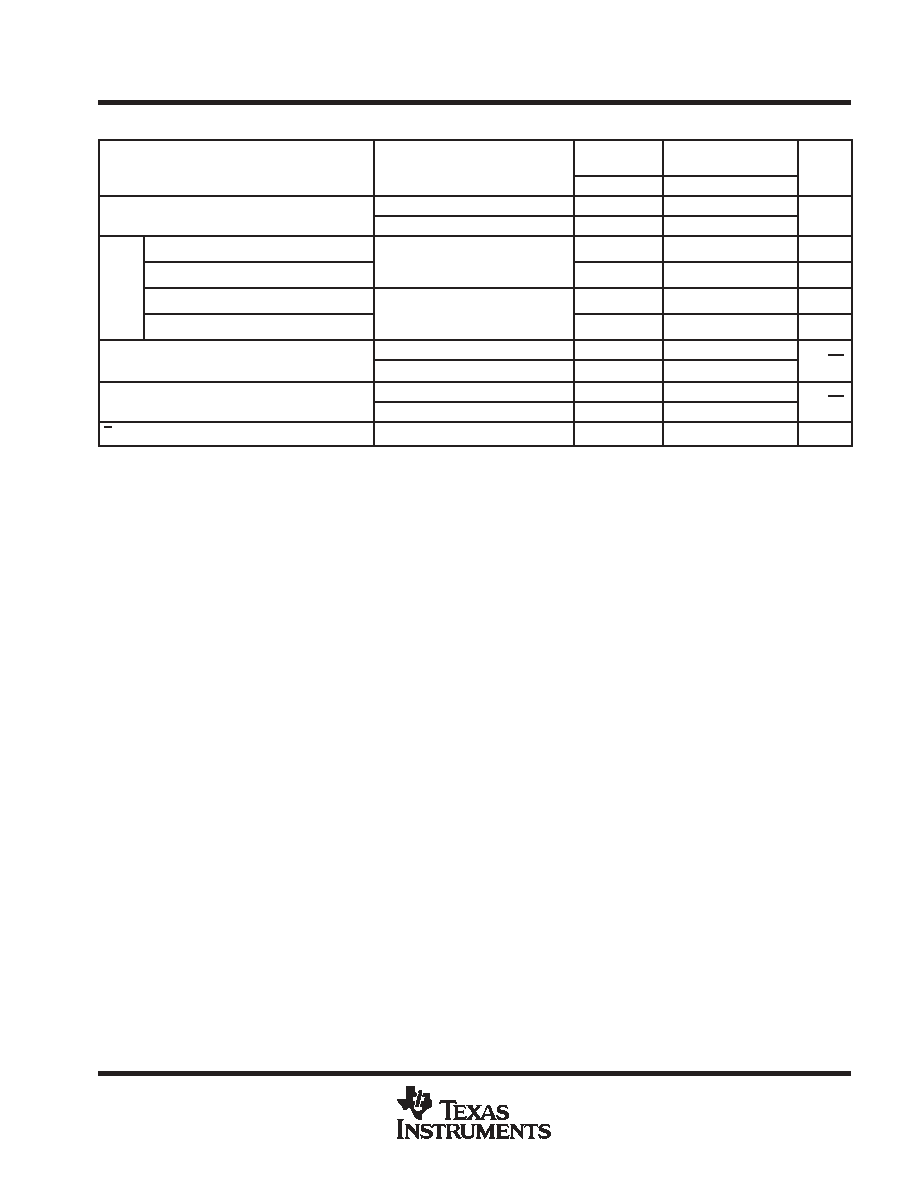
PACKAGING INFORMATION
Orderable Device
Status
(1)
Package
Type
Package
Drawing
Pins Package
Qty
Eco Plan
(2)
Lead/Ball Finish
MSL Peak Temp
(3)
NE5534AD
ACTIVE
SOIC
D
8
75
Pb-Free
(RoHS)
CU NIPDAU
Level-2-250C-1 YEAR
NE5534ADR
ACTIVE
SOIC
D
8
2500
Pb-Free
(RoHS)
CU NIPDAU
Level-2-250C-1 YEAR
NE5534AJG
OBSOLETE
CDIP
JG
8
None
Call TI
Call TI
NE5534AP
ACTIVE
PDIP
P
8
50
Pb-Free
(RoHS)
CU NIPDAU
Level-NC-NC-NC
NE5534D
ACTIVE
SOIC
D
8
75
Pb-Free
(RoHS)
CU NIPDAU
Level-2-250C-1 YEAR
NE5534DR
ACTIVE
SOIC
D
8
2500
Pb-Free
(RoHS)
CU NIPDAU
Level-2-250C-1 YEAR
NE5534IP
OBSOLETE
PDIP
P
8
None
Call TI
Call TI
NE5534P
ACTIVE
PDIP
P
8
50
Pb-Free
(RoHS)
CU NIPDAU
Level-NC-NC-NC
NE5534PSR
ACTIVE
SO
PS
8
2000
Pb-Free
(RoHS)
CU NIPDAU
Level-2-260C-1 YEAR/
Level-1-235C-UNLIM
SA5534AD
ACTIVE
SOIC
D
8
75
Pb-Free
(RoHS)
CU NIPDAU
Level-2-250C-1 YEAR/
Level-1-235C-UNLIM
SA5534ADR
ACTIVE
SOIC
D
8
2500
Pb-Free
(RoHS)
CU NIPDAU
Level-2-250C-1 YEAR/
Level-1-235C-UNLIM
SA5534AP
ACTIVE
PDIP
P
8
50
Pb-Free
(RoHS)
CU NIPDAU
Level-NC-NC-NC
SA5534D
ACTIVE
SOIC
D
8
75
Pb-Free
(RoHS)
CU NIPDAU
Level-2-250C-1 YEAR/
Level-1-235C-UNLIM
SA5534DR
ACTIVE
SOIC
D
8
2500
Pb-Free
(RoHS)
CU NIPDAU
Level-2-250C-1 YEAR/
Level-1-235C-UNLIM
SA5534P
ACTIVE
PDIP
P
8
50
Pb-Free
(RoHS)
CU NIPDAU
Level-NC-NC-NC
SA5534PS
ACTIVE
SO
PS
8
80
Pb-Free
(RoHS)
CU NIPDAU
Level-2-260C-1 YEAR/
Level-1-235C-UNLIM
SA5534PSR
ACTIVE
SO
PS
8
2000
Pb-Free
(RoHS)
CU NIPDAU
Level-2-260C-1 YEAR/
Level-1-235C-UNLIM
(1)
The marketing status values are defined as follows:
ACTIVE: Product device recommended for new designs.
LIFEBUY: TI has announced that the device will be discontinued, and a lifetime-buy period is in effect.
NRND: Not recommended for new designs. Device is in production to support existing customers, but TI does not recommend using this part in
a new design.
PREVIEW: Device has been announced but is not in production. Samples may or may not be available.
OBSOLETE: TI has discontinued the production of the device.
(2)
Eco Plan - May not be currently available - please check
http://www.ti.com/productcontent
for the latest availability information and additional
product content details.
None: Not yet available Lead (Pb-Free).
Pb-Free (RoHS): TI's terms "Lead-Free" or "Pb-Free" mean semiconductor products that are compatible with the current RoHS requirements
for all 6 substances, including the requirement that lead not exceed 0.1% by weight in homogeneous materials. Where designed to be soldered
at high temperatures, TI Pb-Free products are suitable for use in specified lead-free processes.
Green (RoHS & no Sb/Br): TI defines "Green" to mean "Pb-Free" and in addition, uses package materials that do not contain halogens,
including bromine (Br) or antimony (Sb) above 0.1% of total product weight.
(3)
MSL, Peak Temp. -- The Moisture Sensitivity Level rating according to the JEDECindustry standard classifications, and peak solder
temperature.
PACKAGE OPTION ADDENDUM
www.ti.com
4-Mar-2005
Addendum-Page 1

Important Information and Disclaimer:The information provided on this page represents TI's knowledge and belief as of the date that it is
provided. TI bases its knowledge and belief on information provided by third parties, and makes no representation or warranty as to the
accuracy of such information. Efforts are underway to better integrate information from third parties. TI has taken and continues to take
reasonable steps to provide representative and accurate information but may not have conducted destructive testing or chemical analysis on
incoming materials and chemicals. TI and TI suppliers consider certain information to be proprietary, and thus CAS numbers and other limited
information may not be available for release.
In no event shall TI's liability arising out of such information exceed the total purchase price of the TI part(s) at issue in this document sold by TI
to Customer on an annual basis.
PACKAGE OPTION ADDENDUM
www.ti.com
4-Mar-2005
Addendum-Page 2
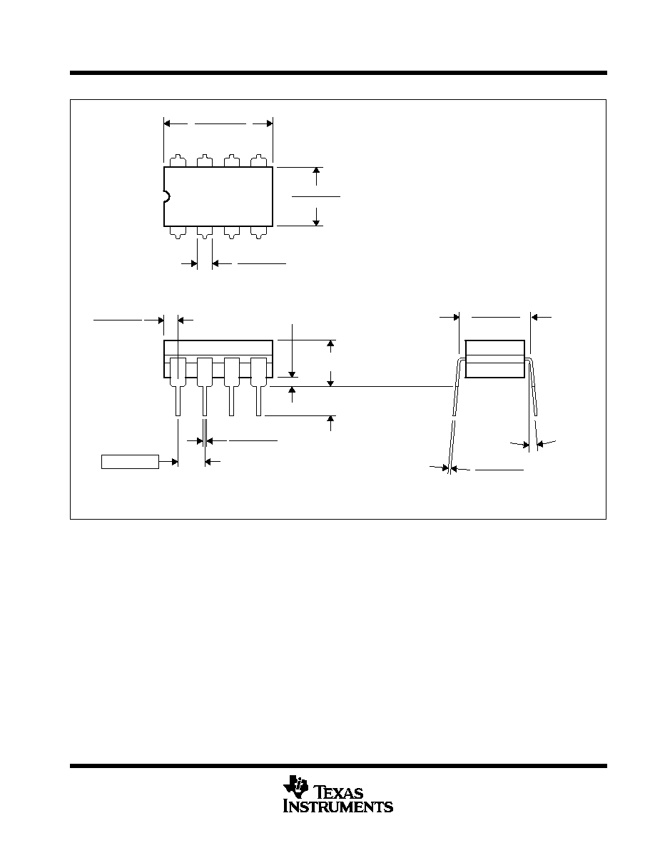
MECHANICAL DATA
MCER001A ≠ JANUARY 1995 ≠ REVISED JANUARY 1997
POST OFFICE BOX 655303
∑
DALLAS, TEXAS 75265
JG (R-GDIP-T8)
CERAMIC DUAL-IN-LINE
0.310 (7,87)
0.290 (7,37)
0.014 (0,36)
0.008 (0,20)
Seating Plane
4040107/C 08/96
5
4
0.065 (1,65)
0.045 (1,14)
8
1
0.020 (0,51) MIN
0.400 (10,16)
0.355 (9,00)
0.015 (0,38)
0.023 (0,58)
0.063 (1,60)
0.015 (0,38)
0.200 (5,08) MAX
0.130 (3,30) MIN
0.245 (6,22)
0.280 (7,11)
0.100 (2,54)
0
∞
≠15
∞
NOTES: A. All linear dimensions are in inches (millimeters).
B. This drawing is subject to change without notice.
C. This package can be hermetically sealed with a ceramic lid using glass frit.
D. Index point is provided on cap for terminal identification.
E. Falls within MIL STD 1835 GDIP1-T8
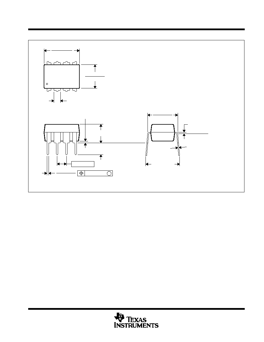
MECHANICAL DATA
MPDI001A ≠ JANUARY 1995 ≠ REVISED JUNE 1999
POST OFFICE BOX 655303
∑
DALLAS, TEXAS 75265
P (R-PDIP-T8)
PLASTIC DUAL-IN-LINE
8
4
0.015 (0,38)
Gage Plane
0.325 (8,26)
0.300 (7,62)
0.010 (0,25) NOM
MAX
0.430 (10,92)
4040082/D 05/98
0.200 (5,08) MAX
0.125 (3,18) MIN
5
0.355 (9,02)
0.020 (0,51) MIN
0.070 (1,78) MAX
0.240 (6,10)
0.260 (6,60)
0.400 (10,60)
1
0.015 (0,38)
0.021 (0,53)
Seating Plane
M
0.010 (0,25)
0.100 (2,54)
NOTES: A. All linear dimensions are in inches (millimeters).
B. This drawing is subject to change without notice.
C. Falls within JEDEC MS-001
For the latest package information, go to http://www.ti.com/sc/docs/package/pkg_info.htm

IMPORTANT NOTICE
Texas Instruments Incorporated and its subsidiaries (TI) reserve the right to make corrections, modifications,
enhancements, improvements, and other changes to its products and services at any time and to discontinue
any product or service without notice. Customers should obtain the latest relevant information before placing
orders and should verify that such information is current and complete. All products are sold subject to TI's terms
and conditions of sale supplied at the time of order acknowledgment.
TI warrants performance of its hardware products to the specifications applicable at the time of sale in
accordance with TI's standard warranty. Testing and other quality control techniques are used to the extent TI
deems necessary to support this warranty. Except where mandated by government requirements, testing of all
parameters of each product is not necessarily performed.
TI assumes no liability for applications assistance or customer product design. Customers are responsible for
their products and applications using TI components. To minimize the risks associated with customer products
and applications, customers should provide adequate design and operating safeguards.
TI does not warrant or represent that any license, either express or implied, is granted under any TI patent right,
copyright, mask work right, or other TI intellectual property right relating to any combination, machine, or process
in which TI products or services are used. Information published by TI regarding third-party products or services
does not constitute a license from TI to use such products or services or a warranty or endorsement thereof.
Use of such information may require a license from a third party under the patents or other intellectual property
of the third party, or a license from TI under the patents or other intellectual property of TI.
Reproduction of information in TI data books or data sheets is permissible only if reproduction is without
alteration and is accompanied by all associated warranties, conditions, limitations, and notices. Reproduction
of this information with alteration is an unfair and deceptive business practice. TI is not responsible or liable for
such altered documentation.
Resale of TI products or services with statements different from or beyond the parameters stated by TI for that
product or service voids all express and any implied warranties for the associated TI product or service and
is an unfair and deceptive business practice. TI is not responsible or liable for any such statements.
Following are URLs where you can obtain information on other Texas Instruments products and application
solutions:
Products
Applications
Amplifiers
amplifier.ti.com
Audio
www.ti.com/audio
Data Converters
dataconverter.ti.com
Automotive
www.ti.com/automotive
DSP
dsp.ti.com
Broadband
www.ti.com/broadband
Interface
interface.ti.com
Digital Control
www.ti.com/digitalcontrol
Logic
logic.ti.com
Military
www.ti.com/military
Power Mgmt
power.ti.com
Optical Networking
www.ti.com/opticalnetwork
Microcontrollers
microcontroller.ti.com
Security
www.ti.com/security
Telephony
www.ti.com/telephony
Video & Imaging
www.ti.com/video
Wireless
www.ti.com/wireless
Mailing Address:
Texas Instruments
Post Office Box 655303 Dallas, Texas 75265
Copyright
2005, Texas Instruments Incorporated