TMS370Cx0x
8-BIT MICROCONTROLLER
SPNS029C ≠ SEPTEMBER 1995 ≠ REVISED FEBRUARY 1997
1
POST OFFICE BOX 1443
∑
HOUSTON, TEXAS 77251≠1443
D
CMOS / EEPROM/ EPROM Technologies on
a Single Device
≠ Mask-ROM Devices for High-Volume
Production
≠ One-Time-Programmable (OTP) EPROM
Devices for Low Volume Production
≠ Reprogrammable EPROM Devices for
Prototyping Purposes
D
Internal System Memory Configurations
≠ On-Chip Program Memory Versions
≠ ROM: 8K Bytes
≠ EPROM: 8K Bytes
≠ Data EEPROM: 256 Bytes
≠ Static RAM: 256 Bytes Usable as
Registers
D
Flexible Operating Features
≠ Low-Power Modes: STANDBY and HALT
≠ Commercial, Industrial, and Automotive
Temperature Ranges
≠ Clock Options
≠ Divide-by-4 (0.5 to 5 MHz SYSCLK)
≠ Divide-by-1 (2 to 5 MHz SYSCLK)
Phase-Locked Loop (PLL)
≠ Supply Voltage (V
CC
) 5 V
±
10%
D
16-Bit General-Purpose Timer
≠ Software Configurable as
a 16-Bit Event Counter, or
a 16-Bit Pulse Accumulator, or
a 16-Bit Input Capture Functions, or
Two Compare Registers, or a
Self-Contained Pulse-Width-Modulation
(PWM) Function
≠ Software Programmable Input Polarity
≠ Eight-Bit Prescaler, Providing a 24-Bit
Real-Time Timer
D
On-Chip 24-Bit Watchdog Timer
≠ EPROM / OTP Devices: Standard
Watchdog
≠ Mask-ROM Devices: Hard Watchdog,
Simple Counter, or Standard Watchdog
D
Flexible Interrupt Handling
≠ Two Software-Programmable Interrupt
Levels
≠ Global- and Individual-Interrupt Masking
≠ Programmable Rising or Falling Edge
Detect
≠ Individual Interrupt Vectors
D
Serial Communications Interface 1 (SCI1)
≠ Asynchronous Mode: 156K bps
Maximum at 5 MHz SYSCLK
≠ Isosynchronous Mode: 25M bps
Maximum at 5 MHz SYSCLK
≠ Full Duplex, Double-Buffered Receiver
(RX) and Transmitter (TX)
≠ Two Multiprocessor Communication
Formats
D
TMS370 Series Compatibility
≠ Register-to-Register Architecture
≠ 256 General-Purpose Registers
≠ 14 Powerful Addressing Modes
≠ Instructions Upwardly Compatible With
All TMS370 Devices
D
CMOS / TTL Compatible I / O Pins / Packages
≠ All Peripheral Function Pins Software
Configurable for Digital I / O
≠ 21 Bidirectional Pins, 1 Input Pin
≠ 28-Pin Plastic and Ceramic Leaded Chip
Carrier Packages
D
Workstation / Personal Computed-Based
Development System
≠ C Compiler and C Source Debugger
≠ Real-time In-Circuit Emulation
≠ Extensive Breakpoint / Trace Capability
≠ Multi-Window User Interface
≠ Microcontroller Programmer
5
6
7
8
9
10
11
3 2 1 28 27
12 13
25
24
23
22
21
20
19
SCITXD
SCICLK
SCIRXD
T1IC / CR
T1PWM
T1EVT
MC
XTAL2 / CLKIN
XTAL1
A6
A5
A4
A3
A2
4
26
14 15 16 1718
SS
A1
A0
D5
INT1
INT2
INT3
V
A7
D7
D6
D3
RESET
D4
FZ AND FN PACKAGES
( TOP VIEW )
CC
V
PRODUCTION DATA information is current as of publication date.
Products conform to specifications per the terms of Texas Instruments
standard warranty. Production processing does not necessarily include
testing of all parameters.
Copyright
©
1997, Texas Instruments Incorporated
Please be aware that an important notice concerning availability, standard warranty, and use in critical applications of
Texas Instruments semiconductor products and disclaimers thereto appears at the end of this data sheet.
TMS370Cx0x
8-BIT MICROCONTROLLER
SPNS029C ≠ SEPTEMBER 1995 ≠ REVISED FEBRUARY 1997
2
POST OFFICE BOX 1443
∑
HOUSTON, TEXAS 77251≠1443
Pin Descriptions
¡¡¡¡¡¡¡¡
¡¡¡¡¡¡¡¡
28 PINS
LCC
¡¡¡
¡¡¡
I / O
¡¡¡¡¡¡¡¡¡¡¡¡¡¡¡¡¡¡¡¡¡¡¡¡¡¡
¡¡¡¡¡¡¡¡¡¡¡¡¡¡¡¡¡¡¡¡¡¡¡¡¡¡
DESCRIPTION
¡¡¡¡¡
¡¡¡¡¡
NAME
¡¡¡¡
¡¡¡¡
NO.
¡¡¡
¡¡¡
¡¡¡¡¡¡¡¡¡¡¡¡¡¡¡¡¡¡¡¡¡¡¡¡¡¡
¡¡¡¡¡¡¡¡¡¡¡¡¡¡¡¡¡¡¡¡¡¡¡¡¡¡
¡¡¡¡¡
¡
¡¡¡
¡
¡
¡¡¡
¡
¡
¡¡¡
¡
¡
¡¡¡
¡
¡
¡¡¡
¡
¡¡¡¡¡
A0
A1
A2
A3
A4
A5
A6
A7
¡¡¡¡
¡
¡¡
¡
¡
¡¡
¡
¡
¡¡
¡
¡
¡¡
¡
¡
¡¡
¡
¡¡¡¡
14
13
11
10
9
8
7
3
¡¡¡
¡
¡
¡
¡
¡
¡
¡
¡
¡
¡
¡
¡
¡
¡
¡
¡¡¡
I / O
¡¡¡¡¡¡¡¡¡¡¡¡¡¡¡¡¡¡¡¡¡¡¡¡¡¡
¡
¡¡¡¡¡¡¡¡¡¡¡¡¡¡¡¡¡¡¡¡¡¡¡¡
¡
¡
¡¡¡¡¡¡¡¡¡¡¡¡¡¡¡¡¡¡¡¡¡¡¡¡
¡
¡
¡¡¡¡¡¡¡¡¡¡¡¡¡¡¡¡¡¡¡¡¡¡¡¡
¡
¡
¡¡¡¡¡¡¡¡¡¡¡¡¡¡¡¡¡¡¡¡¡¡¡¡
¡
¡
¡¡¡¡¡¡¡¡¡¡¡¡¡¡¡¡¡¡¡¡¡¡¡¡
¡
¡¡¡¡¡¡¡¡¡¡¡¡¡¡¡¡¡¡¡¡¡¡¡¡¡¡
Port A is a general-purpose bidirectional I / O port.
¡¡¡¡¡
¡
¡¡¡
¡
¡
¡¡¡
¡
¡¡¡¡¡
D3
D4
D5
D6
D7
¡¡¡¡
¡
¡¡
¡
¡
¡¡
¡
¡¡¡¡
28
26
15
1
2
¡¡¡
¡
¡
¡
¡
¡
¡
¡¡¡
I / O
¡¡¡¡¡¡¡¡¡¡¡¡¡¡¡¡¡¡¡¡¡¡¡¡¡¡
¡
¡¡¡¡¡¡¡¡¡¡¡¡¡¡¡¡¡¡¡¡¡¡¡¡
¡
¡
¡¡¡¡¡¡¡¡¡¡¡¡¡¡¡¡¡¡¡¡¡¡¡¡
¡
¡¡¡¡¡¡¡¡¡¡¡¡¡¡¡¡¡¡¡¡¡¡¡¡¡¡
Port D is a general-purpose bidirectional I / O port. D3 is also configurable as SYSCLK.
¡¡¡¡¡
¡
¡¡¡
¡
¡¡¡¡¡
INT1
INT2
INT3
¡¡¡¡
¡
¡¡
¡
¡¡¡¡
16
17
18
¡¡¡
¡
¡
¡
¡¡¡
I
I / O
I / O
¡¡¡¡¡¡¡¡¡¡¡¡¡¡¡¡¡¡¡¡¡¡¡¡¡¡
¡
¡¡¡¡¡¡¡¡¡¡¡¡¡¡¡¡¡¡¡¡¡¡¡¡
¡
¡¡¡¡¡¡¡¡¡¡¡¡¡¡¡¡¡¡¡¡¡¡¡¡¡¡
External interrupt (non-maskable or maskable) / general-purpose input pin
External maskable interrupt input / general-purpose bidirectional pin
External maskable interrupt input / general-purpose bidirectional pin
¡¡¡¡¡
¡
¡¡¡
¡
¡¡¡¡¡
T1IC / CR
T1PWM
T1EVT
¡¡¡¡
¡
¡¡
¡
¡¡¡¡
22
21
20
¡¡¡
¡
¡
¡
¡¡¡
I / O
¡¡¡¡¡¡¡¡¡¡¡¡¡¡¡¡¡¡¡¡¡¡¡¡¡¡
¡
¡¡¡¡¡¡¡¡¡¡¡¡¡¡¡¡¡¡¡¡¡¡¡¡
¡
¡¡¡¡¡¡¡¡¡¡¡¡¡¡¡¡¡¡¡¡¡¡¡¡¡¡
Timer1 input capture / counter reset input pin / general-purpose bidirectional pin
Timer1 PWM output pin / general-purpose bidirectional pin
Timer1 external event input pin / general-purpose bidirectional pin
¡¡¡¡¡
¡
¡¡¡
¡
¡
¡¡¡
¡
¡¡¡¡¡
SCITXD
SCIRXD
SCICLK
¡¡¡¡
¡
¡¡
¡
¡
¡¡
¡
¡¡¡¡
25
23
24
¡¡¡
¡
¡
¡
¡
¡
¡
¡¡¡
I / O
¡¡¡¡¡¡¡¡¡¡¡¡¡¡¡¡¡¡¡¡¡¡¡¡¡¡
¡
¡¡¡¡¡¡¡¡¡¡¡¡¡¡¡¡¡¡¡¡¡¡¡¡
¡
¡
¡¡¡¡¡¡¡¡¡¡¡¡¡¡¡¡¡¡¡¡¡¡¡¡
¡
¡¡¡¡¡¡¡¡¡¡¡¡¡¡¡¡¡¡¡¡¡¡¡¡¡¡
SCI transmit data output pin, general-purpose bidirectional pin
SCI receive data input pin / general-purpose bidirectional pin
SCI bidirectional serial clock pin / general-purpose bidirectional pin
¡¡¡¡¡
¡¡¡¡¡
RESET
¡¡¡¡
¡¡¡¡
27
¡¡¡
¡¡¡
I / O
¡¡¡¡¡¡¡¡¡¡¡¡¡¡¡¡¡¡¡¡¡¡¡¡¡¡
¡¡¡¡¡¡¡¡¡¡¡¡¡¡¡¡¡¡¡¡¡¡¡¡¡¡
System reset bidirectional pin; as input pin, RESET initializes the microcontroller; as open-drain output,
RESET indicates that an internal failure was detected by watchdog or oscillator fault circuit.
¡¡¡¡¡
¡¡¡¡¡
MC
¡¡¡¡
¡¡¡¡
19
¡¡¡
¡¡¡
I
¡¡¡¡¡¡¡¡¡¡¡¡¡¡¡¡¡¡¡¡¡¡¡¡¡¡
¡¡¡¡¡¡¡¡¡¡¡¡¡¡¡¡¡¡¡¡¡¡¡¡¡¡
Mode control input pin; enables EEPROM write protection override (WPO) mode, also EPROM VPP
¡¡¡¡¡
¡
¡¡¡
¡
¡¡¡¡¡
XTAL2 / CLKIN
XTAL1
¡¡¡¡
¡
¡¡
¡
¡¡¡¡
5
6
¡¡¡
¡
¡
¡
¡¡¡
I
O
¡¡¡¡¡¡¡¡¡¡¡¡¡¡¡¡¡¡¡¡¡¡¡¡¡¡
¡
¡¡¡¡¡¡¡¡¡¡¡¡¡¡¡¡¡¡¡¡¡¡¡¡
¡
¡¡¡¡¡¡¡¡¡¡¡¡¡¡¡¡¡¡¡¡¡¡¡¡¡¡
Internal oscillator crystal input / External clock source input
Internal oscillator output for crystal
¡¡¡¡¡
¡¡¡¡¡
VCC
¡¡¡¡
¡¡¡¡
4
¡¡¡
¡¡¡
¡¡¡¡¡¡¡¡¡¡¡¡¡¡¡¡¡¡¡¡¡¡¡¡¡¡
¡¡¡¡¡¡¡¡¡¡¡¡¡¡¡¡¡¡¡¡¡¡¡¡¡¡
Positive supply voltage
¡¡¡¡¡
¡¡¡¡¡
VSS
¡¡¡¡
¡¡¡¡
12
¡¡¡
¡¡¡
¡¡¡¡¡¡¡¡¡¡¡¡¡¡¡¡¡¡¡¡¡¡¡¡¡¡
¡¡¡¡¡¡¡¡¡¡¡¡¡¡¡¡¡¡¡¡¡¡¡¡¡¡
Ground reference
I = input, O = output
The three-pin SCI configuration is referred to as SCI1.
TMS370Cx0x
8-BIT MICROCONTROLLER
SPNS029C ≠ SEPTEMBER 1995 ≠ REVISED FEBRUARY 1997
3
POST OFFICE BOX 1443
∑
HOUSTON, TEXAS 77251≠1443
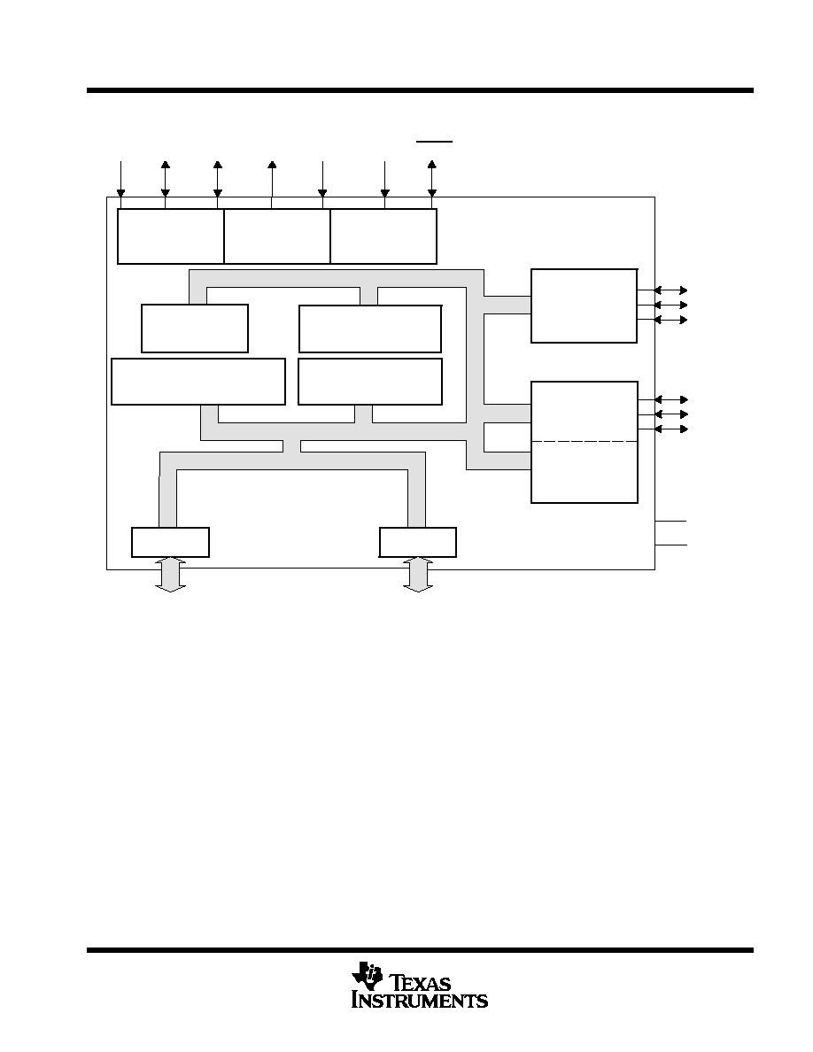
functional block diagram
Interrupts
T1IC/CR
T1EVT
T1PWM
V
System
Control
Clock Options:
Divide-By-4 Or
Divide-By-1 (PLL)
RAM
256 Bytes
CPU
Port A
Port D
Timer 1
Watchdog
INT1
INT2
INT3
XTAL1
XTAL2/
CLKIN
MC
SCIRXD
SCITXD
SCICLK
Serial
Communications
Interface 1
RESET
SS
VCC
Program Memory
ROM: 8K Bytes
EPROM: 8K Bytes
Data EEPROM
0 or 256 Bytes
5
8
description
The TMS370C002, TMS370C302, TMS370C702, and SE370C702 devices are members of the TMS370 family
of single-chip 8-bit microcontrollers. Unless otherwise noted, the term TMS370Cx0x refers to these devices.
The TMS370 family provides cost-effective real-time system control through integration of advanced peripheral
function modules and various on-chip memory configurations.
The TMS370Cx0x family of devices is implemented using high-performance silicon-gate CMOS EPROM and
EEPROM technologies. Low-operating power, wide-operating temperature range, and noise immunity of
CMOS technology coupled with the high performance and extensive on-chip peripheral functions make the
TMS370Cx0x devices attractive in system designs for automotive electronics, industrial motors, computer
peripheral controls, telecommunications, and consumer applications.
All TMS370Cx0x devices contain the following on-chip peripheral modules:
D
Serial communications interface 1 (SCI1)
D
One 16-bit general-purpose timer with an 8-bit prescaler
D
One 24-bit general-purpose watchdog timer
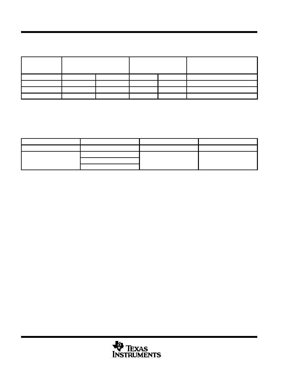
Table 1 provides a memory configuration overview of the TMS370Cx0x devices.
TMS370Cx0x
8-BIT MICROCONTROLLER
SPNS029C ≠ SEPTEMBER 1995 ≠ REVISED FEBRUARY 1997
4
POST OFFICE BOX 1443
∑
HOUSTON, TEXAS 77251≠1443
description (continued)
Table 1. Memory Configurations
¡¡¡¡¡¡¡
¡
¡¡¡¡¡
¡
¡¡¡¡¡¡¡
DEVICE
¡¡¡¡¡¡¡¡¡¡
¡
¡¡¡¡¡¡¡¡
¡
¡¡¡¡¡¡¡¡¡¡
PROGRAM MEMORY
(BYTES)
¡¡¡¡¡¡¡¡¡
¡
¡¡¡¡¡¡¡
¡
¡¡¡¡¡¡¡¡¡
DATA MEMORY
(BYTES)
¡¡¡¡¡¡¡¡¡¡¡
¡
¡¡¡¡¡¡¡¡¡
¡
¡¡¡¡¡¡¡¡¡¡¡
28-PIN PACKAGE
¡¡¡¡¡¡¡
¡¡¡¡¡¡¡
¡¡¡¡¡¡
¡¡¡¡¡¡
ROM
¡¡¡¡¡
¡¡¡¡¡
EPROM
¡¡¡¡¡
¡¡¡¡¡
RAM
¡¡¡¡¡
¡¡¡¡¡
EEPROM
¡¡¡¡¡¡¡¡¡¡¡
¡¡¡¡¡¡¡¡¡¡¡
¡¡¡¡¡¡¡
¡¡¡¡¡¡¡
TMS370C002A
¡¡¡¡¡¡
¡¡¡¡¡¡
8K
¡¡¡¡¡
¡¡¡¡¡
--
¡¡¡¡¡
¡¡¡¡¡
256
¡¡¡¡¡
¡¡¡¡¡
256
¡¡¡¡¡¡¡¡¡¡¡
¡¡¡¡¡¡¡¡¡¡¡
FN ≠ PLCC
¡¡¡¡¡¡¡
TMS370C302A
¡¡¡¡¡¡
8K
¡¡¡¡¡
--
¡¡¡¡¡
256
¡¡¡¡¡
--
¡¡¡¡¡¡¡¡¡¡¡
FN ≠ PLCC
¡¡¡¡¡¡¡
¡¡¡¡¡¡¡
TMS370C702
¡¡¡¡¡¡
¡¡¡¡¡¡
--
¡¡¡¡¡
¡¡¡¡¡
8K
¡¡¡¡¡
¡¡¡¡¡
256
¡¡¡¡¡
¡¡¡¡¡
256
¡¡¡¡¡¡¡¡¡¡¡
¡¡¡¡¡¡¡¡¡¡¡
FN ≠ PLCC
¡¡¡¡¡¡¡
¡¡¡¡¡¡¡
SE370C702
¡¡¡¡¡¡
¡¡¡¡¡¡
--
¡¡¡¡¡
¡¡¡¡¡
8K
¡¡¡¡¡
¡¡¡¡¡
256
¡¡¡¡¡
¡¡¡¡¡
256
¡¡¡¡¡¡¡¡¡¡¡
¡¡¡¡¡¡¡¡¡¡¡
FZ ≠ CLCC
System evaluators and development are for use only in prototype environment and their reliability has not been characterized.
The suffix letter (A) appended to the device name (shown in the first column of Table 1) indicates the
configuration of the device. ROM and EPROM devices have different configurations as indicated in Table 2.
ROM devices with the suffix letter A are configured through a programmable contact during manufacture.
Table 2. Suffix Letter Configuration
DEVICE
WATCHDOG TIMER
CLOCK
LOW-POWER MODE
EPROM without A
Standard
Divide-by-4 (standard oscillator)
Enabled
Standard
Di id b 4
ROM A
Hard
Divide-by-4 or
Divide-by-1 (PLL)
Enabled or disabled
Simple
Divide-by-1 (PLL)
The 8K bytes of mask-programmable ROM in the associated TMS370Cx0x devices are replaced in the
TMS370C702 with 8K bytes of EPROM. All other available memory and on-chip peripherals are identical, with
the exception of no data EEPROM on the TMS370C302 devices. The one-time programmable (OTP)
(TMS370C702) device and reprogrammable device (SE370C702) are available.
TMS370C702 OTP devices are available in plastic packages. This microcontroller is effective to use for
immediate production updates for other members of the TMS370Cx0x family or for low-volume production runs
when the mask charge or cycle time for low-cost mask ROM devices is not practical.
The SE370C702 has a windowed ceramic package to allow reprogramming of the program EPROM memory
during the development-prototyping phase of design. The SE370C702 devices allow quick updates to
breadboards and prototype systems while iterating initial designs.
The TMS370Cx0x family provides two low-power modes (STANDBY and HALT) for applications where
low-power consumption is critical. Both modes stop all CPU activity (that is, no instructions are executed). In
the STANDBY mode, the internal oscillator and the general purpose timer remain active. In the HALT mode,
all device activity is stopped. The device retains all RAM data and peripheral configuration bits throughout both
low-power modes.
The TMS370Cx0x features advanced register-to-register architecture that allows direct arithmetic and logical
operations without requiring an accumulator (for example, ADD R24, R47; add the contents of register 24 to
the contents of register 47 and store the result in register 47). The TMS370Cx0x family is fully
instruction-set-compatible, providing easy transition between members of the TMS370 8-bit microcontroller
family.
The TMS370Cx0x devices have two operational modes of serial communications provided by the SCI1 module.
The SCI1 allows standard RS-232-C communications with other common data transmission equipment.

TMS370Cx0x
8-BIT MICROCONTROLLER
SPNS029C ≠ SEPTEMBER 1995 ≠ REVISED FEBRUARY 1997
5
POST OFFICE BOX 1443
∑
HOUSTON, TEXAS 77251≠1443
description (continued)
The TMS370Cx0x family provides the system designer with an economical, efficient solution to real-time control
applications. The TMS370 family compact development tool (CDT
TM
) solves the challenge of efficiently
developing the software and hardware required to design the TMS370Cx0x into an ever-increasing number of
complex applications. The application source code can be written in assembly and C-language, and the output
code can be generated by the linker. The TMS370 family CDT development tool can communicate through a
standard RS-232-C interface with an existing personal computer. This allows the use of the personal computer
editors and software utilities already familiar to the designer. The TMS370 family CDT emphasizes ease-of-use
through extensive menus and screen windowing so that a system designer with minimal training can begin
developing software. Precise real-time in-circuit emulation and extensive symbolic debug and analysis tools
ensure efficient software and hardware implementation as well as reduced time-to-market cycle.
The TMS370Cx0x family together with the TMS370 family CDT370, design kit, starter kit, software tools, the
SE370C712 reprogrammable devices, comprehensive product documentation, and customer support provide
a complete solution to the needs of the system designer.
central processing unit (CPU)
The CPU used on the TMS370Cx0x device is the high-performance 8-bit TMS370 CPU module. The 'x0x
implements an efficient register-to-register architecture that eliminates the conventional accumulator
bottleneck. The complete 'x0x instruction map is shown in Table 15 in the TMS370Cx0x instruction set overview
section.
The '370Cx0x CPU architecture provides the following components:
CPU registers:
D
A stack pointer that points to the last entry in the memory stack
D
A status register that monitors the operation of the instructions and contains the global interrupt enable bits
D
A program counter (PC) that points to the memory location of the next instruction to be executed
Figure 1 illustrates the CPU registers and memory blocks.
CDT is a trademark of Texas Instruments Incorporated.