TMS370 Microcontroller Family
Extract
Data Book
1997
8-Bit Microcontroller Family

Printed in U.S.A., March 1997
SPND005

General Information
Quality and Reliability
Electrostatic Discharge Guidelines
Mechanical Data
1
2
3
4

TMS370 Microcontroller Family
Data Book
Extract
SPND005
March 1997
Printed on Recycled Paper

IMPORTANT NOTICE
Texas Instruments (TI) reserves the right to make changes to its products or to discontinue any
semiconductor product or service without notice, and advises its customers to obtain the latest
version of relevant information to verify, before placing orders, that the information being relied
on is current.
TI warrants performance of its semiconductor products and related software to the specifications
applicable at the time of sale in accordance with TI's standard warranty. Testing and other quality
control techniques are utilized to the extent TI deems necessary to support this warranty.
Specific testing of all parameters of each device is not necessarily performed, except those
mandated by government requirements.
Certain applications using semiconductor products may involve potential risks of death,
personal injury, or severe property or environmental damage ("Critical Applications").
TI SEMICONDUCTOR PRODUCTS ARE NOT DESIGNED, INTENDED, AUTHORIZED, OR
WARRANTED TO BE SUITABLE FOR USE IN LIFE-SUPPORT APPLICATIONS, DEVICES
OR SYSTEMS OR OTHER CRITICAL APPLICATIONS.
Inclusion of TI products in such applications is understood to be fully at the risk of the customer.
Use of TI products in such applications requires the written approval of an appropriate TI officer.
Questions concerning potential risk applications should be directed to TI through a local SC
sales office.
In order to minimize risks associated with the customer's applications, adequate design and
operating safeguards should be provided by the customer to minimize inherent or procedural
hazards.
TI assumes no liability for applications assistance, customer product design, software
performance, or infringement of patents or services described herein. Nor does TI warrant or
represent that any license, either express or implied, is granted under any patent right, copyright,
mask work right, or other intellectual property right of TI covering or relating to any combination,
machine, or process in which such semiconductor products or services might be or are used.
Copyright
©
1997, Texas Instruments Incorporated

v
INTRODUCTION
The TMS370 Microcontroller Family Data Book from Texas Instruments includes complete
detailed specifications on the TMS370 8-Bit Microcontroller Family product line to include
the following subfamilies TMS370Cx0x, TMS370Cx1x, TMS370Cx2x, TMS370Cx32,
TMS370Cx36, TMS370Cx4x, TMS370Cx5x, TMS370Cx6x, TMS370Cx7x, TMS370Cx8x,
TMS370Cx9x, TMS370CxAx, TMS370CxBx, and TMS370CxCx.
The objective of this manual is to provide the user with complete information on all the
subfamilies contained within the TMS370 Family, enabling selection of a particular device
to suit the user's needs and application much easier.
The data book is divided into the following sections, each of which is described briefly below:
Section 1. General Information ≠ Introduces the TMS370 Family of devices, discusses
the key features and major components of the device family, provides a
functional-block-diagram generalization, and contains an ordering guide showing the
device-numbering convention for all 14 subfamilies. This section also provides a selection
reference guide; a listing of the development system support tools; defines: acronyms, key
terms and signal names; operating conditions and characteristics; and timing conventions.
Section 2. Quality and Reliability ≠ Details the selected processes, standards and
philosophies that Texas Instruments uses to ensure the production of high quality products.
Section 3. Guidelines for Handling Electrostatic-Discharge-Sensitive Devices and
Assemblies ≠ Because the devices included in the TMS370 8-Bit Microcontroller Family
are categorized as Class 2 ESD-sensitive, this section includes the guidelines for the
handling of ESD-sensitive devices.
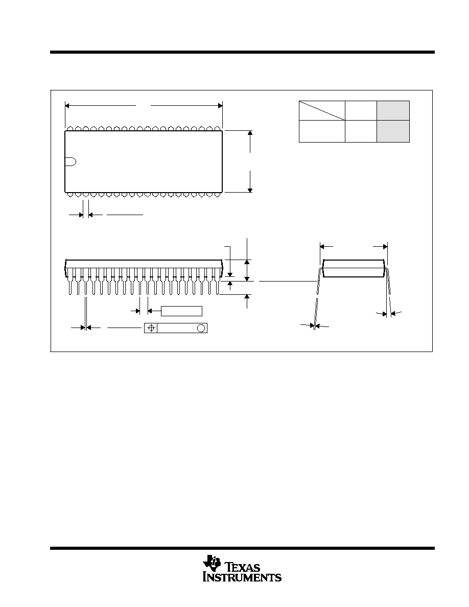
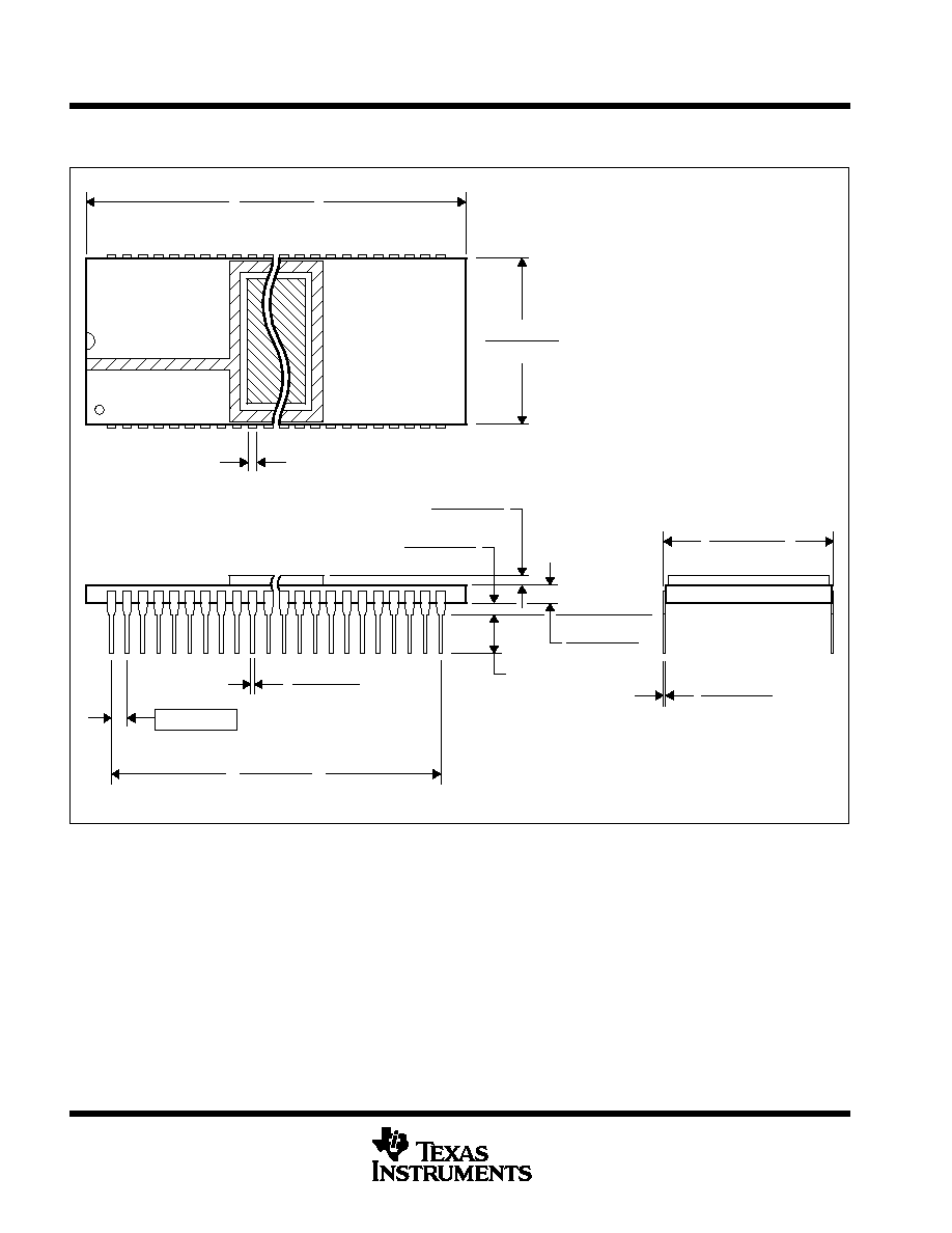
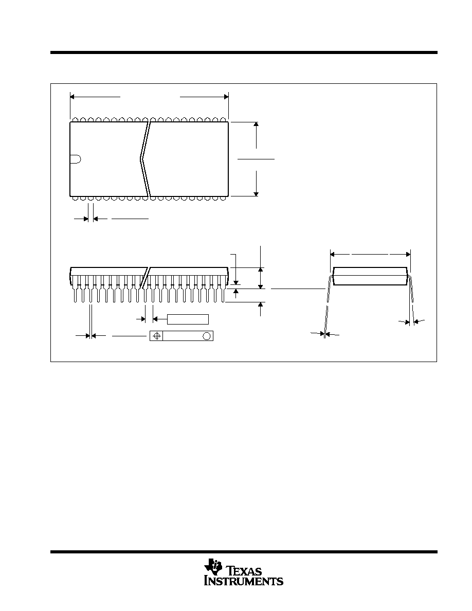
Section 4. Mechanical Data ≠ Shows the detailed mechanical drawing packages and the
associated specifications for each package type utilized in the TMS370 family. This section
also provides a cross-reference table to identify the mechanical package type(s) to a
specific device family.
For ordering information or further assistance, please contact your nearest Texas
Instruments sales office or distributor as listed on the back page of this book.

vi
PRODUCT STAGE STATEMENTS
Product stage statements are used on Texas Instruments data sheets to
indicate the development stage(s) of the product(s) specified in the data
sheets.
If all products specified in a data sheet are at the same development stage,
the appropriate statement from the following list is placed in the lower left
corner of the first page of the data sheet.
PRODUCTION DATA information is current as of publication date.
Products conform to specifications per the terms of Texas Instruments
standard warranty. Production processing does not necessarily include
testing of all parameters.
ADVANCE INFORMATION concerns new products in the sampling or
preproduction phase of development. Characteristic data and other
specifications are subject to change without notice.
PRODUCT PREVIEW information concerns products in the formative
or design phase of development. Characteristic data and other
specifications are design goals. Texas Instruments reserves the right to
change or discontinue these products without notice.
If not all products specified in a data sheet are at the PRODUCTION DATA
stage, then the first statement below is placed in the lower left corner of the
first page of the data sheet. Subsequent pages of the data sheet containing
PRODUCT PREVIEW information or ADVANCE INFORMATION are then
marked in the lower left-hand corner with the appropriate statement given
below:
UNLESS OTHERWISE NOTED this document contains
PRODUCTION DATA information current as of publication date.
Products conform to specifications per the terms of Texas Instruments
standard warranty. Production processing does not necessarily include
testing of all parameters.
ADVANCE INFORMATION concerns new products in the sampling or
preproduction phase of development. Characteristic data and other
specifications are subject to change without notice.
PRODUCT PREVIEW information concerns products in the formative
or design phase of development. Characteristic data and other
specifications are design goals. Texas Instruments reserves the right to
change or discontinue these products without notice.

1≠1
POST OFFICE BOX 1443
∑
HOUSTON, TEXAS 77251≠1443
General Information
Quality and Reliability
Electrostatic Discharge Guidelines
Mechanical Data
1
2
3
4

1≠2
POST OFFICE BOX 1443
∑
HOUSTON, TEXAS 77251≠1443
Contents
Page
Introduction to the TMS370 Family of Devices
1≠3
. . . . . . . . . . . . . . . . . . . . . . . .
Overview
1≠4
. . . . . . . . . . . . . . . . . . . . . . . . . . . . . . . . . . . . . . . . . . . . . . . . . . . . . . . . . .
Typical Applications
1≠4
. . . . . . . . . . . . . . . . . . . . . . . . . . . . . . . . . . . . . . . . . . . . . . . .
Device Categories
1≠5
. . . . . . . . . . . . . . . . . . . . . . . . . . . . . . . . . . . . . . . . . . . . . . . . . .
Key Features
1≠6
. . . . . . . . . . . . . . . . . . . . . . . . . . . . . . . . . . . . . . . . . . . . . . . . . . . . . .
TMS370 Major Components Architecture
1≠7
. . . . . . . . . . . . . . . . . . . . . . . . . . . .
Functional-Block-Diagram Generalization
1≠11
. . . . . . . . . . . . . . . . . . . . . . . . . . .
Device-Numbering Conventions
1≠13
. . . . . . . . . . . . . . . . . . . . . . . . . . . . . . . . . . .
Available Development System Support Tools
1≠14
. . . . . . . . . . . . . . . . . . . . . .
Selection Reference Guide
1≠15
. . . . . . . . . . . . . . . . . . . . . . . . . . . . . . . . . . . . . . . .
Development Systems Support Tools
1≠15
. . . . . . . . . . . . . . . . . . . . . . . . . . . . . .
Third-Party Support
1≠21
. . . . . . . . . . . . . . . . . . . . . . . . . . . . . . . . . . . . . . . . . . . . . .
Operating Conditions and Characteristics
1≠22
. . . . . . . . . . . . . . . . . . . . . . . . .
Timing Conventions
1≠23
. . . . . . . . . . . . . . . . . . . . . . . . . . . . . . . . . . . . . . . . . . . . . .
Related Documentation From Texas Instruments
1≠27
. . . . . . . . . . . . . . . . . . .
For Further Assistance
1≠28
. . . . . . . . . . . . . . . . . . . . . . . . . . . . . . . . . . . . . . . . . . .
Glossary /Symbols, Terms, and Definitions
1≠29
. . . . . . . . . . . . . . . . . . . . . . . . .
1
General Information

INTRODUCTION TO THE TMS370 FAMILY OF DEVICES
1≠3
POST OFFICE BOX 1443
∑
HOUSTON, TEXAS 77251≠1443
introduction to the TMS370 family of devices
This section discusses the key features and major components of the TMS370 8-Bit Microcontroller subfamilies
('x0x, 'x1x, 'x2x, 'x32, 'x36, 'x4x, ..., 'xCx) and includes a functional-block-diagram generalization that depicts
all available modules, noting that no one device contains all the available modules. The section concludes with
the device-numbering convention and a list of other Texas Instruments related documents.
This section covers the following topics:
D
Overview
D
Typical Applications
D
Device Categories
D
Key Features
D
TMS370 Major Components Architecture
≠
CPU
≠
Register File (RF)
≠
RAM
≠
Data EEPROM
≠
Program Memory (ROM/EPROM)
≠
Input/Output Ports
≠
Timer 1
≠
Timer 2n (A and B)
≠
Watchdog Timer
≠
Programmable Acquisition and Control Timer (PACT)
≠
Serial Communications Interface (SCI1 or SCI2)
≠
Serial Peripheral Interface (SPI)
≠
Analog-to-Digital Converter (ADC1, ADC2 or ADC3) Modules
D
Functional-Block-Diagram Generalization
D
Device-Numbering Conventions
D
Available Development-System-Support Tools
D
Section Reference Guide
D
Development-System-Support Tools
D
Operating Conditions and Characteristics
D
Timing Conventions
D
Related Documentation from Texas Instruments
D
For Further Assistance
D
Glossary / Symbols, Terms, and Definitions

OVERVIEW
1≠4
POST OFFICE BOX 1443
∑
HOUSTON, TEXAS 77251≠1443
overview
The TMS370 family consists of very large scaled integration (VLSI), 8-bit, complementary metal oxide
semiconductor (CMOS) microcontrollers with on-chip EEPROM storage and peripheral-support functions.
These devices offer superior performance in complex, real-time control applications in demanding
environments and are available in mask-programmable ROM and EPROM.
In a continual effort to improve its products, Texas Instruments has added new, more robust features to the
TMS370 family of devices that are designed to enhance performance and enable new application technologies.
These added features include new watchdog modes and low-power modes for mask-ROM devices. All family
members are software compatible, so that many existing applications can be run on the improved devices
without modification of software. (Refer to the associated data sheets for more information on compatibility.)
In expanding its powerful TMS370 family of microcontrollers, TI
TM
offers many new configurable devices for
specific applications. As microcontrollers have evolved, TI has added multiple peripheral functions to chips that
originally had only a central processing unit (CPU), memory, and I/O blocks. Now, with the high-performance,
software-compatible TMS370 microcontrollers, over 130 standard products are available. Also, up to
27 function modules can be used to configure a new device quickly, easily, and cost-effectively for any
applications.
The TMS370 family is supported fully by TI development tools that facilitate simplified software development
for prompt market introduction of new products. These tools include an assembler, an optimizing C compiler,
a linker, a C source debugger, a design kit,
a starter kit, and a third-party microcontroller programmer from
BP Microsystems. All of these tools work together by using an IBM
TM
-compatible
personal computer (PC) as
the host and the central control element. This allows the user to select the host computer and text management
as well as editing tools according to system requirements.
Additionally, the TMS370 in-circuit emulator [XDS
TM
-- extended development support, and
CDT370 compact
development tool (CDT
TM
)] allows the user to immediately begin designing, testing, and debugging the system
upon specification. The reason for this is straightforward: the emulator itself is modular and configurable,
thereby eliminating the need to produce a new emulator for each TMS370 configuration.
typical applications
The TMS370 family of devices is the ideal choice for the applications shown in Table 1 because the newly added
features (like the addition of multiple peripheral functions per device) have expanded the TMS370 family of
microcontrollers, enhanced its performance, and opened up new application technologies.
Table 1. Typical Applications for TMS370 Family of Microcontroller Devices
¡¡¡¡¡¡¡¡¡
¡¡¡¡¡¡¡¡¡
APPLICATION AREA
¡¡¡¡¡¡¡¡¡¡¡¡¡¡¡¡¡¡
¡¡¡¡¡¡¡¡¡¡¡¡¡¡¡¡¡¡
APPLICATIONS
¡¡¡¡¡¡¡¡¡
¡
¡¡¡¡¡¡¡
¡
¡
¡¡¡¡¡¡¡
¡
¡¡¡¡¡¡¡¡¡
Automotive
¡¡¡¡¡¡¡¡¡
¡
¡¡¡¡¡¡¡
¡
¡
¡¡¡¡¡¡¡
¡
¡¡¡¡¡¡¡¡¡
Climate control systems
Cruise control
Entertainment systems
Instrumentation
¡¡¡¡¡¡¡¡¡¡
¡
¡¡¡¡¡¡¡¡
¡
¡
¡¡¡¡¡¡¡¡
¡
¡¡¡¡¡¡¡¡¡¡
Navigational systems
Engine control
Antilock braking
¡¡¡¡¡¡¡¡¡
¡
¡¡¡¡¡¡¡
¡
¡¡¡¡¡¡¡¡¡
Computer
¡¡¡¡¡¡¡¡¡
¡
¡¡¡¡¡¡¡
¡
¡¡¡¡¡¡¡¡¡
Keyboards
Peripheral interface control
¡¡¡¡¡¡¡¡¡¡
¡
¡¡¡¡¡¡¡¡
¡
¡¡¡¡¡¡¡¡¡¡
Disk controllers
Terminals
¡¡¡¡¡¡¡¡¡
¡
¡¡¡¡¡¡¡
¡
¡¡¡¡¡¡¡¡¡
Industrial
¡¡¡¡¡¡¡¡¡
¡
¡¡¡¡¡¡¡
¡
¡¡¡¡¡¡¡¡¡
Motor control
Temperature controllers
Process control
¡¡¡¡¡¡¡¡¡¡
¡
¡¡¡¡¡¡¡¡
¡
¡¡¡¡¡¡¡¡¡¡
Meter control
Medical instrumentation
Security systems
¡¡¡¡¡¡¡¡¡
¡
¡¡¡¡¡¡¡
¡
¡¡¡¡¡¡¡¡¡
Telecommunications
¡¡¡¡¡¡¡¡¡
¡
¡¡¡¡¡¡¡
¡
¡¡¡¡¡¡¡¡¡
Modems
Intelligent phones
Intelligent line card control
¡¡¡¡¡¡¡¡¡¡
¡
¡¡¡¡¡¡¡¡
¡
¡¡¡¡¡¡¡¡¡¡
Telecopiers
Debit cards
TI, XDS, and CDT are trademarks of Texas Instruments Incorporated.
IBM is a trademark of International Business Machines Corp.

DEVICE CATEGORIES
1≠5
POST OFFICE BOX 1443
∑
HOUSTON, TEXAS 77251≠1443
device categories
The TMS370 category of devices is divided into 14 subfamilies (see Table 2). All the subfamilies are supported
by a full complement of development support tools, which are listed in Table 5.
Table 2. TMS370 Family Categories and Their Corresponding Devices
¡¡¡¡¡¡¡¡¡
¡¡¡¡¡¡¡¡¡
FAMILY
¡¡¡¡¡¡¡¡¡¡¡¡¡¡¡¡¡¡¡¡¡¡¡¡¡
¡¡¡¡¡¡¡¡¡¡¡¡¡¡¡¡¡¡¡¡¡¡¡¡¡
DEVICES INCLUDED
TMS370Cx0x
TMS370C002A
TMS370C302A
TMS370C702
SE370C702
¡¡¡¡¡¡¡¡¡
¡
¡¡¡¡¡¡¡
¡
¡¡¡¡¡¡¡¡¡
TMS370Cx1x
¡¡¡¡¡¡¡¡¡¡¡¡¡¡¡¡¡¡¡¡¡¡¡¡¡
¡
¡¡¡¡¡¡¡¡¡¡¡¡¡¡¡¡¡¡¡¡¡¡¡
¡
¡¡¡¡¡¡¡¡¡¡¡¡¡¡¡¡¡¡¡¡¡¡¡¡¡
TMS370C010A
TMS370C012A
TMS370C310A
TMS370C311A
TMS370C312A
TMS370C712A
TMS370C712B
SE370C712A
SE370C712B
TMS370Cx2x
TMS370C020A
TMS370C022A
TMS370C320A
TMS370C322A
TMS370C722
SE370C722
¡¡¡¡¡¡¡¡¡
¡¡¡¡¡¡¡¡¡
TMS370Cx32
¡¡¡¡¡¡¡¡¡¡¡¡¡¡¡¡¡¡¡¡¡¡¡¡¡
¡¡¡¡¡¡¡¡¡¡¡¡¡¡¡¡¡¡¡¡¡¡¡¡¡
TMS370C032A
TMS370C732A
TMS370C332A
SE370C732A
TMS370Cx36
TMS370C036A
TMS370C736A
SE370C736A
¡¡¡¡¡¡¡¡¡
¡
¡¡¡¡¡¡¡
¡
¡¡¡¡¡¡¡¡¡
TMS370Cx4x
¡¡¡¡¡¡¡¡¡¡¡¡¡¡¡¡¡¡¡¡¡¡¡¡¡
¡
¡¡¡¡¡¡¡¡¡¡¡¡¡¡¡¡¡¡¡¡¡¡¡
¡
¡¡¡¡¡¡¡¡¡¡¡¡¡¡¡¡¡¡¡¡¡¡¡¡¡
TMS370C040A
TMS370C042A
TMS370C340A
TMS370C342A
TMS370C742A
SE370C742A
TMS370Cx5x
TMS370C050A
TMS370C052A
TMS370C056A
TMS370C058A
TMS370C059A
TMS370C150A
TMS370C156A
TMS370C250A
TMS370C256A
TMS370C350A
TMS370C352A
TMS370C353A
TMS370C356A
TMS370C358A
TMS370C452A
TMS370C456A
TMS370C756A
TMS370C758A
TMS370C758B
TMS370C759A
SE370C756A
SE370C758A
SE370C758B
SE370C759A
¡¡¡¡¡¡¡¡¡
¡
¡¡¡¡¡¡¡
¡
¡¡¡¡¡¡¡¡¡
TMS370Cx6x
¡¡¡¡¡¡¡¡¡¡¡¡¡¡¡¡¡¡¡¡¡¡¡¡¡
¡
¡¡¡¡¡¡¡¡¡¡¡¡¡¡¡¡¡¡¡¡¡¡¡
¡
¡¡¡¡¡¡¡¡¡¡¡¡¡¡¡¡¡¡¡¡¡¡¡¡¡
TMS370C067A
TMS370C068A
TMS370C069A
TMS370C768A
TMS370C769A
SE370C768A
SE370C769A
TMS370Cx7x
TMS370C077A
TMS370C777A
SE370C777A
¡¡¡¡¡¡¡¡¡
TMS370Cx8x
¡¡¡¡¡¡¡¡¡¡¡¡¡¡¡¡¡¡¡¡¡¡¡¡¡
TMS370C080
TMS370C380A
TMS370C686A
SE370C686A
TMS370Cx9x
TMS370C090A
TMS370C792
SE370C792
¡¡¡¡¡¡¡¡¡
¡¡¡¡¡¡¡¡¡
TMS370CxAx
¡¡¡¡¡¡¡¡¡¡¡¡¡¡¡¡¡¡¡¡¡¡¡¡¡
¡¡¡¡¡¡¡¡¡¡¡¡¡¡¡¡¡¡¡¡¡¡¡¡¡
TMS370C3A7A
TMS370CxBx
TMS370C0B6A
¡¡¡¡¡¡¡¡¡
¡¡¡¡¡¡¡¡¡
TMS370CxCx
¡¡¡¡¡¡¡¡¡¡¡¡¡¡¡¡¡¡¡¡¡¡¡¡¡
¡¡¡¡¡¡¡¡¡¡¡¡¡¡¡¡¡¡¡¡¡¡¡¡¡
TMS370C3C0A
TMS370C6C2A
SE370C6C2A
These system evaluators are used only in a prototype environment. Their reliability has not been characterized.

KEY FEATURES
1≠6
POST OFFICE BOX 1443
∑
HOUSTON, TEXAS 77251≠1443
key features
The TMS370 family is based on a register-to-register architecture that allows access to a register file (up to
256 bytes) in a single bus cycle. On-chip memory includes program memory (mask ROM or EPROM), static
RAM, standby RAM, and data EEPROM.
The versatile on-chip peripheral functions include an analog-to-digital converter (ADC1, ADC2, or ADC3), a
serial communications interface (SCI1 or SCI2), a serial peripheral interface (SPI), three different timer modules
(T1, T2A, and T2B), and up to 55 digital input / output (I / O) pins. The number and type of peripheral functions
(modules) is dependent on the TMS370 subfamily.
The following are key features of the TMS370 device family (not all features are available for all devices):
D
Compatibility for supporting software migration between current and future microcontrollers
D
CMOS EPROM technology for providing reprogrammable EPROM and one-time programmable (OTP)
program memory for prototypes and for small-volume or quick-turn production
D
CMOS EEPROM technology for providing EEPROM programming with a single 5-V supply
D
ADC technology for converting analog signals to digital values
D
Static RAM/register file registers that offer numerous memory options
D
Standby RAM that offers data protection in power-off condition
D
Programmable (asynchronous and isosynchronous
) built-in serial communications interface for control of
timing, data format, and protocol
D
Serial peripheral interface for providing single-mode synchronous data transmission from the CPUs to any
external peripheral devices
D
Flexible operating features:
≠
Power-reduction-standby and halt modes
≠
Temperature options:
0
∞
C to 70
∞
C operating temperature (L)
≠ 40
∞
C to 85
∞
C operating temperature (A)
≠ 40
∞
C to 105
∞
C operating temperature (T)
≠
Input clock frequency options:
Divide-by-4 ( 0.5 MHz to 5 MHz SYSCLK ) standard oscillator
Divide-by-1 ( 2 MHz to 5 MHz SYSCLK) phase-locked loop (PLL)
≠
Operating voltage range: 5 V +10%
D
Flexible interrupt handling for design flexibility:
≠
Two programmable interrupt levels
≠
Programmable rising-edge or falling-edge detect
D
System integrity features that increase flexibility during the software development phase:
≠
Oscillator fault detection
≠
Privileged mode lockout
≠
Watchdog timer
≠
Memory security (for ROM)
Isosynchronous = isochronous

TMS370 MAJOR COMPONENTS ARCHITECTURE
1≠7
POST OFFICE BOX 1443
∑
HOUSTON, TEXAS 77251≠1443
key features (continued)
D
Memory-mapped ports for easy addressing
D
An optimizing C compiler that translates ANSI C programs into TMS370 assembly language source
D
A high-level language debugger that lets the user refine and correct code
D
A modular library for quickly changing the device configurations
D
18 addressing modes that use eight formats, including:
≠
Implied
≠
Register-to-register arithmetic
≠
Indirect addressing
≠
Indexed and indirect branches and calls
≠
PC relative
D
250-mA typical latch-up immunity at 25
∞
C
D
Electrostatic discharge (ESD) protection that exceeds 2,000 V per MIL-STD-883C method 3015, making
the TMS370 families Class 2 ESD-sensitive devices
TMS370 major components architecture
In addition to the features listed in the key features section, the TMS370 family members have the following
architectural features. Not all features (key or architectural) are applicable to all devices. The selection reference
guide (see Table 4) summarizes the following features and identifies the applicable devices associated with
those features.
CPU
The TMS370 8-bit CPU has a status register, program-counter register, and stack pointer. The CPU uses the
register file as working registers that are accessed on the internal bus in one bus cycle. The 8-bit internal bus
also allows access to memory and to the peripheral interfaces. TMS370Cx5x and TMS370Cx6x devices all
allow external memory expansion through ports A, B, C, and D.
register file (RF)
The register file is located at the beginning of the TMS370 memory map. Register-access instructions in the
TMS370 instruction set allow access to any of the first 256 registers (if available) in one bus cycle. This segment
of the memory map is used as general-purpose RAM and as the stack.
RAM
RAM modules, other than those contained in the register file, are mapped after the register file. The TMS370
accesses this RAM in two cycles.
data EEPROM
With the exception of the TMS370CxAx and TMS370CxCx device groups, certain devices in the TMS370 family
have EEPROM.The data EEPROM modules provide in-circuit programmability and data retention in power-off
mode. The modules contain 256 or 512 bytes of EEPROM. This memory is useful for storing constants and
infrequently changed variables that are required by the application program. The EEPROM can be programmed
and erased by using available EEPROM programmers or by the TMS370 device under program control.

TMS370 MAJOR COMPONENTS ARCHITECTURE
1≠8
POST OFFICE BOX 1443
∑
HOUSTON, TEXAS 77251≠1443
program memory (ROM/EPROM)
The program memory provides alternatives to meet the needs of different applications. The program memory
modules presently contain 2K, 4K, 8K, 16K, 24K
, 32K, or 48K bytes of memory. The program memory in
TMS370C6xx, SE370C6xx, TMS370C7xx, and SE370C7xx devices is EPROM. EPROM devices in a
windowed ceramic package can be programmed, erased, and reprogrammed for prototyping. EPROM devices
in a non-windowed plastic package are one-time programmable (OTP) devices that are used for small
production runs. In the TMS370C0xx, TMS370C3xx, and TMS370C4xx devices, the program memory is
mask-ROM that is programmed at the factory. ROM devices are appropriate for large-volume production.
input/output ports
The TMS370 family of devices has a varying number of I/O ports that have various port widths. Table 3 lists the
available I/O port widths, by the number of bits, for each of the TMS370 subfamilies.
Table 3. Bits Per Port for TMS370 Devices
SUBFAMILIES
BITS FOR PORTS A ≠ H
SUBFAMILIES
A
B
C
D
G
H
'x0x, 'x1x
8
5
'x2x
8
8
1
5
'x32
8
4
'x36
8
5
'x4x
8
3
5
'x5x ≠ (64 pins)
8
8
8
6
'x5x ≠ (68 pins)
8
8
8
8
'x6x
8
8
8
5
'x7x ≠ (64 pins)
8
8
8
6
6
'x7x ≠ (68 pins)
8
8
8
8
6
'x8x ≠ (40 pins)
8
8
6
5
'x8x ≠ (44 pins)
8
8
8
5
'x9x
8
5
'xAx
8
8
1
5
'xBx ≠ (64 pins)
8
8
8
6
8
1
'xBx ≠ (68 pins)
8
8
8
8
8
1
'xCx
8
4
For all subfamilies, the ports for these microcontrollers can be programmed, bit by bit, to function as either digital
input or digital output.
These ports can be configured by the software as the data, control, and address buses for external memory. Any
bits not needed for external memory can be programmed to be either digital input or digital output.
timer 1
Timer 1 is a 16-bit timer that can be configured in the following ways:
D
A programmable 8-bit prescaler (provides a 24-bit real-time timer) that determines the independent clock
sources for the general-purpose timer and the watchdog (WD) timer
D
A 16-bit event timer to keep a cumulative total of the transitions
D
A 16-bit pulse accumulator to measure the pulse-input width
D
A 16-bit input-capture function that latches the counter value on the occurrence of an external input
D
Two 16-bit compare registers that trigger when the counter matches the contents of a compare register
D
A self-contained pulse-width modulated (PWM) output control function

TMS370 MAJOR COMPONENTS ARCHITECTURE
1≠9
POST OFFICE BOX 1443
∑
HOUSTON, TEXAS 77251≠1443
timer 1 (continued)
The results of these operations can generate an interrupt to the CPU, set flag bits, reset the timer counter, toggle
an I/O line, or generate PWM outputs. Timer 1 can provide up to 200 ns of resolution with a 5-MHz system clock
(SYSCLK).
timer 2n (A and B)
Timer 2A and 2B are 16-bit timers that can be configured in the following ways:
D
Four independent clock sources for the general-purpose timer
D
A
16-bit event timer, to keep a cumulative total of the transitions
D
A16-bit pulse accumulator, to measure the pulse-input width
D
Two 16-bit input-capture devices that change a counter value on the occurrence of an external input
D
Two 16-bit compare registers that trigger when a counter matches the contents of a compare register
D
A
self-contained PWM output controller
The results of the timer 2A and 2B operations can generate an interrupt to the CPU, set flag bits, reset the timer
counter, toggle an I/O line, or generate PWM outputs. Timers 2A and 2B can provide up to 200 ns of resolution
with a 5-MHz system clock (SYSCLK).
watchdog timer
The watchdog (WD) timer helps ensure system integrity. The WD timer can be programmed to generate a
hardware reset upon a time-out condition. The WD function provides a hardware monitor over the software to
help avoid losing a program. If not needed as a WD, this timer can be used as a general-purpose timer.
programmable acquisition and control timer (PACT)
The PACT module in the 'x32 and 'x36 subfamilies is a programmable timing module that uses some of the
on-chip RAM to store its commands and the timer values
. Only the TMS370Cx36 device offers the 256-byte
standby RAM that protects stored data against power failures. The PACT module offers the following:
D
Input capture on up to six pins, four of which may have a programmable prescaler
D
One input-capture pin that can drive an 8-bit event counter
D
Up to eight timer-driven outputs
D
Timer capability of up to 20 bits
D
Interaction between event counter and timer activity
D
18 independent interrupt vectors to allow better servicing of events
D
Watchdog with selectable time-out period
D
Mini-SCI (serial communications interface) that works as a full duplex UART (universal asynchronous
receiver transmitter)
Once set up, the PACT requires no CPU overhead except to service interrupts.

TMS370 MAJOR COMPONENTS ARCHITECTURE
1≠10
POST OFFICE BOX 1443
∑
HOUSTON, TEXAS 77251≠1443
serial communications interface (SCI1 or SCI2)
The term SCI is used frequently to refer to SCI1 and SCI2. The SCI1 and SCI2 modules are built-in serial
interfaces. The SCI1 has a 3-pin configuration and SCI2 has a 2-pin configuration. Both offer the following
features:
D
Programmable to be asynchronous (up to 156 Kbps)
D
Full duplex, double-buffered receive (Rx) and transmit (Tx)
D
Programmable format with error-checking capabilities
The following feature is available only on the SCI1 module:
D
Programmable to be isosynchronous (up to 2.5 Mbps)
The SCI1 and SCI2 modules program and control all timing, data format, and protocol factors. The CPU takes
part in the serial communications only:
D
To write data transmitted to the registers in the SCI
D
To read received data from the registers in the SCI when interrupted
serial peripheral interface (SPI)
The SPI module is a built-in serial interface that facilitates communication between the network master, slave
CPUs, and the external peripheral devices. The SPI module provides synchronous data transmission of up to
2.5 Mbps. Like the SCI, the SPI is set up by software. Once setup, the CPU takes no part in timing, data format,
or protocol. Also, like the SCI, the CPU reads and writes to memory-mapped registers to receive and transmit
data. An SPI interrupt alerts the CPU when received data is ready.
analog-to-digital converter (ADC1, ADC2, ADC3) modules
The 8-bit ADC
modules perform successive approximation conversion. The term ADC is a general term used
for ADC1, ADC2, and ADC3 modules. The ADCs offer the following number of input channels for each of the
specified microcontroller families:
D
ADC1 offers the following:
≠
Four channels in the 40-pin devices of the 'x4x subfamily,
≠
Eight channels in the 44-pin devices of the 'x4x, 'x32, and 'x36 subfamilies
≠
Eight channels in the 64-pin and 68-pin devices of the 'x5x, 'x6x, 'x7x, and 'xBx subfamilies
D
ADC2 offers four channels in the 28-pin devices of the 'xCx subfamily
D
ADC3 offers 15 channels in the 40-pin and 44-pin devices of the 'x9x subfamily
The reference source and input channel are selectable. The user can program the conversion result to be the
ratio of the input voltage to the reference voltage or the ratio of one analog input to another. Input lines that are
not required for analog-to-digital conversion can be programmed to be digital input lines.
For a detailed explanation on any of the major components of the TMS370 device family, see the
TMS370 8-Bit
Microcontroller User's Guide (literature number SPNU127) or to the specific subfamily data sheet.
For more details on the programming of the TMS370 family or for further expansion on the applications of these
devices, see the paragraph in this section on related documentation from Texas Instruments.

FUNCTIONAL-BLOCK-DIAGRAM GENERALIZATION
1≠11
POST OFFICE BOX 1443
∑
HOUSTON, TEXAS 77251≠1443
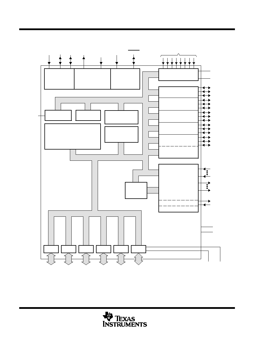
functional-block-diagram generalization
This section contains a functional-block-diagram generalization for the TMS370 microcontroller subfamilies
(that is, 'x0x, 'x1x, 'x2x, 'x32, 'x36, 'x4x, ..., 'xCx). Because this diagram is a generalization, it depicts all the
modules available for the TMS370 families, noting that no one TMS370 device contains all available options.
The diagram also shows the basic internal connections among the major architectural features that are
identified in the selection guide (see Table 4). For a functional block diagram of a specific TM370 subfamily, the
pinouts, the descriptions of the pinouts, and descriptions of the external connection names, refer to the
applicable data sheet.

FUNCTIONAL-BLOCK-DIAGRAM GENERALIZATION
1≠12
POST OFFICE BOX 1443
∑
HOUSTON, TEXAS 77251≠1443
functional-block-diagram generalization (continued)
¡
¡
¡
¡
¡
¡¡
¡
¡
¡¡
¡
¡
¡
¡¡
¡
¡
¡¡
¡
¡
Interrupts
System
Control
Clock Options
Divide-by-4 or
Divide-by-1(PLL)
Serial Peripheral
Interface
Program Memory
ROM: 2K, 4K, 8K, 12K, 16K, 24K,
32K or 48K Bytes
EPROM: 8K, 16K, 24K, 32K or
48K Bytes
Watchdog
Timer 1
Serial
Communications
Interface
Timer 2A
Timer 2B
PACT
Mini SCI
Watchdog
128 Bytes
Dual-Port
RAM
Data EEPROM
256 or 512 Bytes
RAM 128, 256,
384, 512, 1K or
3.5K Bytes
CPU
VSS2 VCC2
VCC1
VSS1
1
8
8
8
8
SCIRXD
SCITXD
OP8
OP1
CP6
CP1
T1PWM
T1EVT
T1IC / CR
T2AIC2 / PWM
T2AEVT
T2AIC1 / CR
T2BIC2 / PWM
T2BEVT
T2BIC1 / CR
SCICLK
SCITXD
SCIRXD
SPICLK
SPISIMO
SPISOMI
8
Port A
Port B
Port C
Port D
Port G
Port H
VSS3
VCC3
Standby RAM
256 Bytes
Memory Expansion
Data
Address LSbyte
Address MSbyte
Control
VCCSTBY
INT1
INT2 INT3
XTAL1
XTAL2 /
CLKIN
MC
RESET
E0 ≠ E7
or
AN0 ≠ AN7
Analog-to-Digital
Converter
Not available on all devices; see the selection reference guide (Table 4).

DEVICE-NUMBERING CONVENTIONS
1≠13
POST OFFICE BOX 1443
∑
HOUSTON, TEXAS 77251≠1443
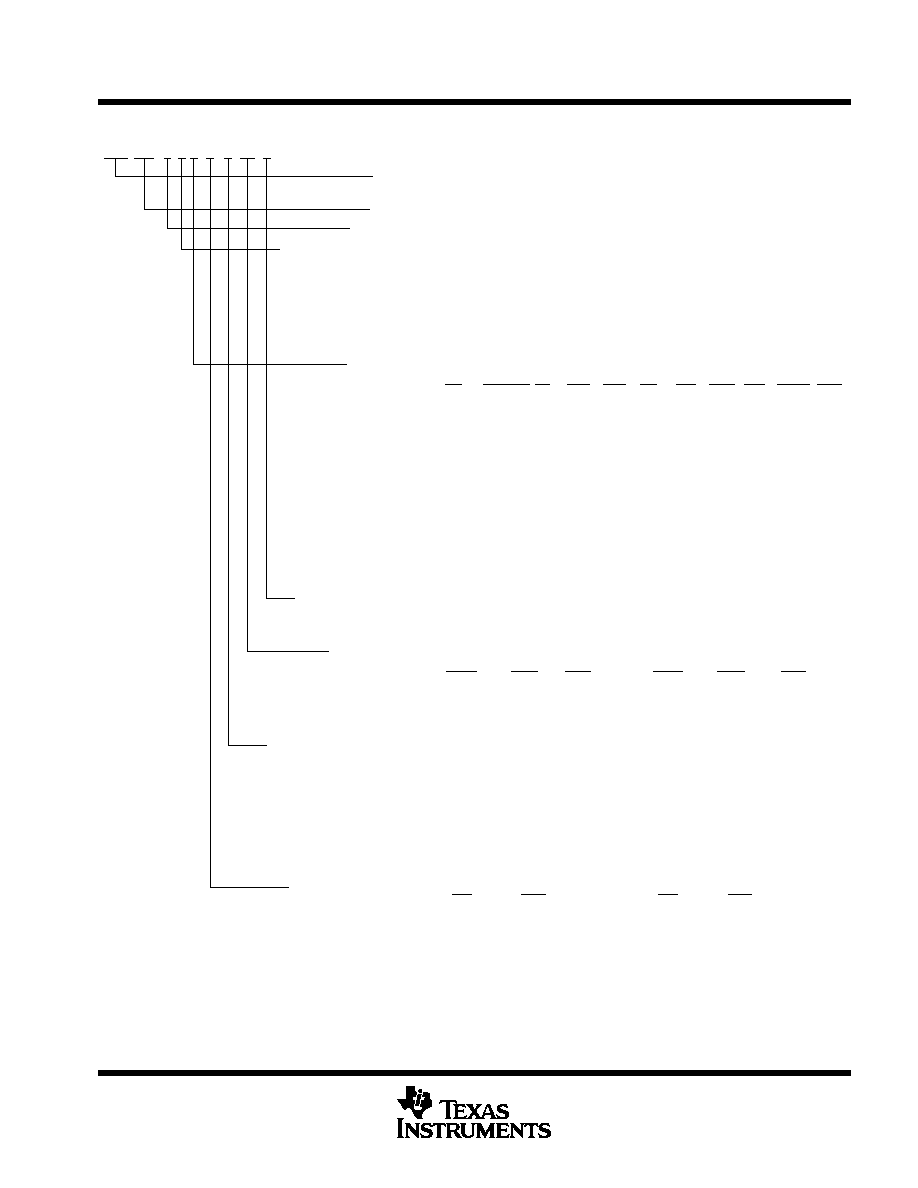
device-numbering conventions
Prefix: TMS = Qualified
SE = System evaluator (window EEPROM)
Family:
370 = TMS370 Microcontroller Family
Technology:
C = Complementary Metal-Oxide Semiconductor (CMOS)
Program Memory Types:
0 = Mask-ROM and EEPROM
1 = ROM-less, no Data EEPROM
2 = ROM-less, and EEPROM
3 = Mask-ROM, no Data EEPROM
4 = ROM Memory with Security and EEPROM
6 = EPROM, no Data EEPROM
7 = EPROM and EEPROM
Device Type:
External
Extra
No
Memory T1
T2A
T2B
SCI
SPI
ADC PIO PACT Pins
0 =
SCI1
28
1 =
28
2 =
SCI1
40/44
3 =
ADC1
44
4 =
SCI1
ADC1
40/44
5 =
SCI1
ADC1
64/68
6 =
SCI1
ADC1
68
7 =
ADC1
64/68
8 =
40/44
9 =
ADC3
40/44
A =
SCI1
40
B =
ADC1
64/68
C =
SCI2
ADC2
28
Temperature Ranges:
A =
≠ 40
∞
C to 85
∞
C
L =
0
∞
C to 70
∞
C
T =
≠ 40
∞
C to 105
∞
C
Package Types:
TI
Pkg
No.
TI
Pkg
No.
Code
Type
Pins
Code
Type
Pins
JD
=
CDIP
28/40
N
=
PDIP
28/40
FZ
=
CLCC
28/44/68
FN
=
PLCC
28/44/68
JC
=
CSDIP
40
NJß =
PSDIP
40
JN
=
CSDIP
64
NM
=
PSDIP
64
ROM and EEPROM Option:
For ROM:
A = Selectable clock as
4 or
1 (PLL) and a watchdog timer
configured as one of the three mask options: standard
watchdog, hard watchdog, or simple counter.
None = Standard watchdog and
4 OSC, low-power modes enabled
For ROM-less:
A = Standard watchdog and
4 OSC, low-power modes enabled
For EPROM:
A = Standard watchdog and
4 OSC, low-power modes enabled
B = Hard watchdog and
1 PLL, low-power modes enabled
None = Standard watchdog and
4 OSC, low-power modes enabled
Program Memory Size:
No.
Size
No.
Size
0
=
4K bytes
6
=
16K bytes
1
=
2K bytes
7
=
24K bytes
2
=
8K bytes
8
=
32K bytes
3
=
12K bytes
9
=
48K bytes
Extra peripheral I/O
For device type No. 3 the TMS370Cx32 device has no SPI; the TMS370Cx36 device has an SPI.
ß NJ package was formerly known as N2.
TMS 370 C 7 1 2 A FN T
Figure 1. TMS370C Family Nomenclature

AVAILABLE DEVELOPMENT SYSTEM SUPPORT TOOLS
1≠14
POST OFFICE BOX 1443
∑
HOUSTON, TEXAS 77251≠1443
available development system support tools
The TMS370 family is fully supported by TI development tools that facilitate simplified software development
for prompt market introduction of new products. These tools include an assembler, an optimizing C compiler,
a linker, a C source debugger, a design kit,
a starter kit, and a third-party microcontroller programmer from BP
Microsystems. All of these tools work together by using an IBM-compatible
PC as the host and central control
element. This allows the user to select the host computer and text management as well as editing tools
according to system requirements.
Additionally, the TMS370 in-circuit emulator (XDS and
CDT370) allows the user to immediately begin designing,
testing, and debugging the system upon specification. The reason for this is straightforward: the emulator itself
is modular and configurable, thereby eliminating the need to produce a new emulator for each TMS370
configuration.
For a list of the available development system support tools, identified by device category, refer to the TMS370
Development System Support Tools table (see Table 5) or to the specific TMS370 subfamily data sheet.
For more detailed information on the development system support tools, refer to the
TMS370 8-Bit
Microcontroller User's Guide (literature number SPNU127) or to the documents listed in the section titled related
documentation from Texas Instruments.

SELECTION REFERENCE GUIDE
1≠15
POST OFFICE BOX 1443
∑
HOUSTON, TEXAS 77251≠1443
selection reference guide
The TMS370 8-Bit Microcontroller Product Selection Guide Configurations Table, commonly called the
Selection Reference Guide (see Table 4), provides the user with an easy-to-use guide that includes the
following specific device information by subfamilies: product family description (device type, part number,
package and temperature options, and pin count); memory [program memory (ROM, EPROM), data memory
(EEPROM, RAM) and any capability of off-chip memory expansion]; and peripherals (timers, serial interfaces,
A / D channels, I / O, clock generators, and OTP and reprogrammable devices). The following symbol footnotes
are used in Table 4:
Packages: FN = PLCC, FZ = CLCC, N = PDIP, JD = CDIP, NJ = PSDIP (formerly N2), JC = CSDIP, NM = PSDIP, JN = CSDIP
Temperatures: ROM device types have L = 0
∞
C to +70
∞
C, A = ≠ 40
∞
C to +85
∞
C, and T = ≠ 40
∞
C to +105
∞
C temperature options; ROM-less, OTP
and UV-EPROM device types only have T.
ß PACT SCI: PACT includes a mini-SCI. SCI1 module has 3-pin configuration while SCI2 module has 2-pin configuration.
∂ RAM: Includes 256 bytes of standby RAM
# Memory: Includes secured memory feature
|| Max Freq: Supports maximum operating frequency of 3 MHz SYSCLK
k
PACT WDOG: PACT includes a watchdog timer
h
ADC1 Channels: 8 channels A / D for 44 pin package, 4 channels A / D for 40 pin package
Timers: Timer 1 (T1) includes a watchdog timer programmable as a general purpose 16-bit timer
44/40 Packages: 44 pins for FN, FZ packages. 40 pins for N, JD, NJ (formerly N2), JC packages.
68/64 Packages: 68 pins for FN, FZ packages. 64 pins for NM, JN packages
• TMS370CxCx SCI: Operable in asynchronous mode only
Converter Socket: Requires a TMDS37788OTP converter socket
Requires software modification (see the
TMS370CxBx Data Sheet (literature number SPNS038))
Table 4 is a continuous table and only the applicable symbol footnotes are listed on each page.
development systems support tools
The TMS370 development system support tools listing shown in Table 5 identifies the available development
support tools (by tool description and part number) for each of the TMS370 subfamilies ('x0x, 'x1x, 'x2x, 'x32,
'x36,
...
, 'xCx).

SELECTION REFERENCE GUIDE
T
emp
l
ate
R
e
l
ease
D
ate:
7
≠
11
≠
94
1≠16
POST
OFFICE BOX 1443 HOUST
ON,
TEXAS
77251≠1443
∑
Table 4. TMS370 8-Bit Microcontroller Product Configurations
DEVICE
TYPE
PART NUMBER
"yy "= PACKAGE
"z" TEMP
PACKAGE
OPTIONS
"yy"
PACKAGE
PIN COUNT
PROGRAM
MEMORY
(BYTES)
DATA MEMORY
(BYTES)
OFF-CHIP
MEM EXP
(BYTES)
TIMERS
SERIAL
INTERFACEß
A/D
CHANNELS
I/O
CLOCK
GENERATOR
OTP AND
REPROGRAMMABLE
DEVICES
TYPE
"z" =TEMP
"yy"
PIN COUNT
ROM
EPROM
EEPROM
RAM
(BYTES)
INTERFACE
CHANNELS
GENERATOR
DEVICES
TMS370Cx0x
ROM
TMS370C302Ayyz
FN
28
8K
256
T1
SCI1
22
˜
4 or PLL
C702
ROM
TMS370C002Ayyz
FN
28
8K
256
256
T1
SCI1
22
˜
4 or PLL
C702
OTP
TMS370C702yyz
FN
28
8K
256
256
T1
SCI1
22
˜
4
--
UV-EPROM
SE370C702yyz
FZ
28
8K
256
256
T1
SCI1
22
˜
4
--
TMS370Cx1x
ROM
TMS370C311Ayyz
FN / N
28
2K
128
T1
SPI
22
˜
4 or PLL
C712
ROM
TMS370C310Ayyz
FN / N
28
4K
128
T1
SPI
22
˜
4 or PLL
C712
ROM
TMS370C010Ayyz
FN / N
28
4K
256
128
T1
SPI
22
˜
4 or PLL
C712
ROM
TMS370C312Ayyz
FN / N
28
8K
128
T1
SPI
22
˜
4 or PLL
C712
ROM
TMS370C012Ayyz
FN / N
28
8K
256
256
T1
SPI
22
˜
4 or PLL
C712
OTP
TMS370C712Ayyz
FN / N
28
8K
256
256
T1
SPI
22
˜
4
--
OTP
TMS370C712Byyz
FN / N
28
8K
256
256
T1
SPI
22
PLL
--
UV-EPROM
SE370C712Ayyz
FZ / JD
28
8K
256
256
T1
SPI
22
˜
4
--
UV-EPROM
SE370C712Byyz
FZ / JD
28
8K
256
256
T1
SPI
22
PLL
--
TMS370Cx2x
ROM
TMS370C320Ayyz
FN / N / NJ
44 / 40
4K
256
T1
SPI / SCI1
34
˜
4 or PLL
C722
ROM
TMS370C322Ayyz
FN / N / NJ
44 / 40
8K
256
T1
SPI / SCI1
34
˜
4 or PLL
C722
ROM
TMS370C020Ayyz
FN / N / NJ
44 / 40
4K
256
256
T1
SPI / SCI1
34
˜
4 or PLL
C722
ROM
TMS370C022Ayyz
FN / N / NJ
44 / 40
8K
256
256
T1
SPI / SCI1
34
˜
4 or PLL
C722
OTP
TMS370C722yyz
FN / N / NJ
44 / 40
8K
256
256
T1
SPI / SCI1
34
˜
4
--
UV-EPROM
SE370C722yyz
FZ / JD / JC
44 / 40
8K
256
256
T1
SPI / SCI1
34
˜
4
--
Packages: FN = PLCC, FZ = CLCC, N = PDIP, JD = CDIP, NJ = PSDIP (formerly N2), JC = CSDIP, NM = PSDIP, JN = CSDIP
Temperatures: ROM device types have L = 0
∞
C to +70
∞
C, A = ≠ 40
∞
C to +85
∞
C, and T = ≠ 40
∞
C to +105
∞
C temperature options; ROM-less, OTP and UV-EPROM device types only have T.
ß
PACT SCI: PACT includes a mini-SCI. SCI1 module has 3-pin configuration while SCI2 module has 2-pin configuration.
Timers: Timer 1 (T1) includes a watchdog timer programmable as a general purpose 16-bit timer
44/40 Packages: 44 pins for FN, FZ packages. 40 pins for N, JD, NJ (formerly N2), JC packages.

SELECTION REFERENCE GUIDE
POST
OFFICE BOX 1443 HOUST
ON,
TEXAS
77251≠1443
∑
1≠17
Table 4. TMS370 8-Bit Microcontroller Product Configurations (Continued)
DEVICE
TYPE
PART NUMBER
"yy "= PACKAGE
"z" TEMP
PACKAGE
OPTIONS
"yy"
PACKAGE
PIN
COUNT
PROGRAM
MEMORY
(BYTES)
DATA MEMORY
(BYTES)
OFF-CHIP
MEM EXP
(BYTES)
TIMERS
SERIAL
INTERFACEß
A/D
CHANNELS
I/O
CLOCK
GENERATOR
OTP AND
REPROGRAMMABLE
DEVICES
TYPE
"z" =TEMP
"yy"
COUNT
ROM
EPROM
EEPROM
RAM
(BYTES)
INTERFACE
CHANNELS
GENERATOR
DEVICES
TMS370Cx3x
ROM
TMS370C332Ayyz
FN
44
8K
256
PACT
k
PACT
ADC1/8
23
˜
4 or PLL
C732
ROM
TMS370C032Ayyz
FN
44
8K
256
256
PACT
k
PACT
ADC1/8
23
˜
4 or PLL
C732
ROM
TMS370C036Ayyz
FN
44
16K
256
512
∂
PACT
k
SPI / PACT
ADC1/8
25
˜
4 or PLL
C736
OTP
TMS370C732Ayyz
FN
44
8K
256
256
PACT
k
PACT
ADC1/8
23
˜
4
--
OTP
TMS370C736Ayyz
FN
44
16K
256
512
∂
PACT
k
SPI / PACT
ADC1/8
25
˜
4
--
UV-EPROM
SE370C732Ayyz
FZ
44
8K
256
256
PACT
k
PACT
ADC1/8
23
˜
4
--
UV-EPROM
SE370C736Ayyz
FZ
44
16K
256
512
∂
PACT
k
SPI / PACT
ADC1/8
25
˜
4
--
TMS370Cx4x
ROM
TMS370C340Ayyz
FN / N / NJ
44 / 40
4K
256
T1 / T2a
SCI1
ADC1/8, 4
h
36 / 32
˜
4 or PLL
C742
ROM
TMS370C342Ayyz
FN / N / NJ
44 / 40
8K
256
T1 / T2a
SCI1
ADC1/8, 4
h
36 / 32
˜
4 or PLL
C742
ROM
TMS370C040Ayyz
FN / N / NJ
44 / 40
4K
256
256
T1 / T2a
SCI1
ADC1/8, 4
h
36 / 32
˜
4 or PLL
C742
ROM
TMS370C042Ayyz
FN / N / NJ
44 / 40
8K
256
256
T1 / T2a
SCI1
ADC1/8, 4
h
36 / 32
˜
4 or PLL
C742
OTP
TMS370C742Ayyz
FN / N / NJ
44 / 40
8K
256
256
T1 / T2a
SCI1
ADC1/8, 4
h
36 / 32
˜
4
--
UV-EPROM
SE370C742Ayyz
FZ / JD / JC
44 / 40
8K
256
256
T1 / T2a
SCI1
ADC1/8, 4
h
36 / 32
˜
4
--
TMS370Cx5x
ROM-less
TMS370C150Ayyz
FN
68
256
56K
T1 / T2a
SPI / SCI1
ADC1/8
55
˜
4
C756
ROM-less
TMS370C250Ayyz
FN
68
256
256
56K
T1 / T2a
SPI / SCI1
ADC1/8
55
˜
4
C756
ROM-less
TMS370C156Ayyz
FN
68
512
56K
T1 / T2a
SPI / SCI1
ADC1/8
55
˜
4
C756
ROM-less
TMS370C256Ayyz
FN
68
512
512
56K
T1 / T2a
SPI / SCI1
ADC1/8
55
˜
4
C756
ROM
TMS370C350Ayyz
FN / NM
68 / 64
4K
256
112K
T1 / T2a
SPI / SCI1
ADC1/8
55 / 53
˜
4 or PLL
C756
ROM
TMS370C050Ayyz
FN / NM
68 / 64
4K
256
256
112K
T1 / T2a
SPI / SCI1
ADC1/8
55 / 53
˜
4 or PLL
C756
ROM
TMS370C352Ayyz
FN / NM
68 / 64
8K
256
112K
T1 / T2a
SPI / SCI1
ADC1/8
55 / 53
˜
4 or PLL
C756
ROM
TMS370C052Ayyz
FN / NM
68 / 64
8K
256
256
112K
T1 / T2a
SPI / SCI1
ADC1/8
55 / 53
˜
4 or PLL
C756
ROM
TMS370C452Ayyz
FN
68
8K
#
256
256
112K
T1 / T2a
SPI / SCI1
ADC1/8
55
˜
4 or PLL
C756
ROM
TMS370C353Ayyz
FN
68
12K
1 536
112K
T1 / T2a
SPI / SCI1
ADC1/8
55
˜
4 or PLL
C759
Packages: FN = PLCC, FZ = CLCC, N = PDIP, JD = CDIP, NJ = PSDIP (formerly N2), JC = CSDIP, NM = PSDIP, JN = CSDIP
Temperatures: ROM device types have L = 0
∞
C to +70
∞
C, A = ≠ 40
∞
C to +85
∞
C, and T = ≠ 40
∞
C to +105
∞
C temperature options; ROM-less, OTP and UV-EPROM device types only have T.
ß
PACT SCI: PACT includes a mini-SCI. SCI1 module has 3-pin configuration while SCI2 module has 2-pin configuration.
∂
RAM: Includes 256 bytes of standby RAM
#
Memory: Includes secured memory feature
k
PACT WDOG: PACT includes a watchdog timer
h
ADC1 Channels: 8 channels A / D for 44 pin package, 4 channels A / D for 40 pin package
Timers: Timer 1 (T1) includes a watchdog timer programmable as a general purpose 16-bit timer
44/40 Packages: 44 pins for FN, FZ packages. 40 pins for N, JD, NJ (formerly N2), JC packages.
68/64 Packages: 68 pins for FN, FZ packages. 64 pins for NM, JN packages

SELECTION REFERENCE GUIDE
T
emp
l
ate
R
e
l
ease
D
ate:
7
≠
11
≠
94
1≠18
POST
OFFICE BOX 1443 HOUST
ON,
TEXAS
77251≠1443
∑
Table 4. TMS370 8-Bit Microcontroller Product Configurations (Continued)
DEVICE
TYPE
PART NUMBER
"yy "= PACKAGE
"z" TEMP
PACKAGE
OPTIONS
"yy"
PACKAGE
PIN
COUNT
PROGRAM
MEMORY
(BYTES)
DATA MEMORY
(BYTES)
OFF-
CHIP
MEM EXP
TIMERS
SERIAL
INTERFACEß
A/D
CHANNELS
I/O
CLOCK
GENERATOR
OTP AND
REPROGRAMMABLE
DEVICES
TYPE
"z" =TEMP
"yy"
COUNT
ROM
EPROM
EEPROM
RAM
MEM EXP
(BYTES)
INTERFACE
CHANNELS
GENERATOR
DEVICES
TMS370Cx5x (CONTINUED)
ROM
TMS370C356Ayyz
FN / NM
68 / 64
16K
512
112K
T1 / T2a
SPI / SCI1
ADC1/8
55 / 53
˜
4 or PLL
C756
ROM
TMS370C456Ayyz
FN
68
16K#
512
512
112K
T1 / T2a
SPI / SCI1
ADC1/8
55
˜
4 or PLL
C756
ROM
TMS370C056Ayyz
FN / NM
68 / 64
16K
512
512
112K
T1 / T2a
SPI / SCI1
ADC1/8
55 / 53
˜
4 or PLL
C756
ROM
TMS370C358Ayyz
FN / NM
68 / 64
32K
1 024
64K
T1 / T2a
SPI / SCI1
ADC1/8
55 / 53
˜
4 or PLL
C758
ROM
TMS370C058Ayyz
FN / NM
68 / 64
32K
256
1 024
64K
T1 / T2a
SPI / SCI1
ADC1/8
55 / 53
˜
4 or PLL
C758
ROM
TMS370C059Ayyz
FN
68
48K||
256
3 584
20K
T1 / T2a
SPI / SCI1
ADC1/8
55
˜
4 or PLL
C759
OTP
TMS370C756Ayyz
FN / NM
68 / 64
16K
512
512
112K
T1 / T2a
SPI / SCI1
ADC1/8
55 / 53
˜
4
--
OTP
TMS370C758Ayyz
FN / NM
68 / 64
32K
256
1 024
64K
T1 / T2a
SPI / SCI1
ADC1/8
55 / 53
˜
4
--
OTP
TMS370C758Byyz
FN / NM
68 / 64
32K
256
1 024
64K
T1 / T2a
SPI / SCI1
ADC1/8
55 / 53
PLL
--
OTP
TMS370C759Ayyz
FN
68
48K||
256
3 584
20K
T1 / T2a
SPI / SCI1
ADC1/8
55
˜
4
--
UV-EPROM
SE370C756Ayyz
FZ / JN
68 / 64
16K
512
512
112K
T1 / T2a
SPI / SCI1
ADC1/8
55 / 53
˜
4
--
UV-EPROM
SE370C758Ayyz
FZ / JN
68 / 64
32K
256
1 024
64K
T1 / T2a
SPI / SCI1
ADC1/8
55 / 53
˜
4
--
UV-EPROM
SE370C758Byyz
FZ / JN
68 / 64
32K
256
1 024
64K
T1 / T2a
SPI / SCI1
ADC1/8
55 / 53
PLL
--
UV-EPROM
SE370C759Ayyz
FZ
68
48K||
256
3 584
20K
T1 / T2a
SPI / SCI1
ADC1/8
55
˜
4
--
TMS370Cx6x
ROM
TMS370C067Ayyz
FN
68
24K
256
1 024
24K
T1 / T2a / T2b
SPI / SCI1
ADC1/8
55
˜
4 or PLL
C768
ROM
TMS370C068Ayyz
FN
68
32K
256
1 024
24K
T1 / T2a / T2b
SPI / SCI1
ADC1/8
55
˜
4 or PLL
C768
ROM
TMS370C069Ayyz
FN
68
48K||
256
3 584
8K
T1 / T2a / T2b
SPI / SCI1
ADC1/8
55
˜
4 or PLL
C769
OTP
TMS370C768Ayyz
FN
68
32K
256
1 024
24K
T1 / T2a / T2b
SPI / SCI1
ADC1/8
55
˜
4
--
OTP
TMS370C769Ayyz
FN
68
48K||
256
3 584
8K
T1 / T2a / T2b
SPI / SCI1
ADC1/8
55
˜
4
--
UV-EPROM
SE370C768Ayyz
FZ
68
32K
256
1 024
24K
T1 / T2a / T2b
SPI / SCI1
ADC1/8
55
˜
4
--
UV-EPROM
SE370C769Ayyz
FZ
68
48K||
256
3 584
8K
T1 / T2a / T2b
SPI / SCI1
ADC1/8
55
˜
4
--
Packages: FN = PLCC, FZ = CLCC, N = PDIP, JD = CDIP, NJ = PSDIP (formerly N2), JC = CSDIP, NM = PSDIP, JN = CSDIP
Temperatures: ROM device types have L = 0
∞
C to +70
∞
C, A = ≠ 40
∞
C to +85
∞
C, and T = ≠ 40
∞
C to +105
∞
C temperature options; ROM-less, OTP and UV-EPROM device types only have T.
ß
PACT SCI: PACT includes a mini-SCI. SCI1 module has 3-pin configuration while SCI2 module has 2-pin configuration.
||
Max Freq: Supports maximum operating frequency of 3 MHz SYSCLK
Timers: Timer 1 (T1) includes a watchdog timer programmable as a general purpose 16-bit timer
68/64 Packages: 68 pins for FN, FZ packages. 64 pins for NM, JN packages

SELECTION REFERENCE GUIDE
POST
OFFICE BOX 1443 HOUST
ON,
TEXAS
77251≠1443
∑
1≠19
Table 4. TMS370 8-Bit Microcontroller Product Configurations (Continued)
DEVICE
TYPE
PART NUMBER
"yy "= PACKAGE
"z" TEMP
PACKAGE
OPTIONS
"yy"
PACKAGE
PIN COUNT
PROGRAM
MEMORY
(BYTES)
DATA MEMORY
(BYTES)
OFF-CHIP
MEM EXP
(BYTES)
TIMERS
SERIAL
INTERFACEß
A/D
CHANNELS
I/O
CLOCK
GENERATOR
OTP AND
REPROGRAMMABLE
DEVICES
TYPE
"z" =TEMP
"yy"
PIN COUNT
ROM
EPROM
EEPROM
RAM
(BYTES)
INTERFACE
CHANNELS
GENERATOR
DEVICES
TMS370Cx7x
ROM
TMS370C077Ayyz
FN / NM
68 / 64
24K
256
512
T1 / T2a
ADC1/8
55 / 53
˜
4 or PLL
C777
OTP
TMS370C777Ayyz
FN / NM
68 / 64
24K
256
512
T1 / T2a
ADC1/8
55 / 53
˜
4
--
UV-EPROM
SE370C777Ayyz
FZ / JN
68 / 64
24K
256
512
T1 / T2a
ADC1/8
55 / 53
˜
4
--
TMS370Cx8x
ROM
TMS370C380Ayyz
FN
44
4K
128
T1
35
˜
4 or PLL
C686
ROM
TMS370C080yyz
N
40
4K
256
128
T1
33
˜
4
C758
OTP
TMS370C686Ayyz
FN
44
16K
256
T1
35
˜
4
--
UV-EPROM
SE370C686Ayyz
FZ
44
16K
256
T1
35
˜
4
--
TMS370Cx9x
ROM
TMS370C090Ayyz
FN / NJ
44 / 40
4K
256
128
T1
ADC3/15
25
˜
4 or PLL
C792
OTP
TMS370C792yyz
FN / NJ
44 / 40
8K
256
128
T1
ADC3/15
25
˜
4
--
UV-EPROM
SE370C792yyz
FZ / JC
44 / 40
8K
256
128
T1
ADC3/15
25
˜
4
--
TMS370CxAx
ROM
TMS370C3A7Ayyz
N
40
24K
512
T1 / T2a
SCI1
34
˜
4 or PLL
C758
TMS370CxBx
ROM
TMS370C0B6Ayyz
FN / NM
68 / 64
16K
256
384
T1
ADC1/8
55 / 53
˜
4 or PLL
C758
TMS370CxCx
ROM
TMS370C3C0Ayyz
FN / N
28
4K
128
T1
SCI2
•
ADC2/4
22
˜
4 or PLL
C6C2
OTP
TMS370C6C2Ayyz
FN / N
28
8K
128
T1
SCI2
•
ADC2/4
22
˜
4
--
UV-EPROM
SE370C6C2Ayyz
FZ / JD
28
8K
128
T1
SCI2
•
ADC2/4
22
˜
4
--
Packages: FN = PLCC, FZ = CLCC, N = PDIP, JD = CDIP, NJ = PSDIP (formerly N2), JC = CSDIP, NM = PSDIP, JN = CSDIP
Temperatures: ROM device types have L = 0
∞
C to +70
∞
C, A = ≠ 40
∞
C to +85
∞
C, and T = ≠ 40
∞
C to +105
∞
C temperature options; ROM-less, OTP and UV-EPROM device types only have T.
ß
PACT SCI: PACT includes a mini-SCI. SCI1 module has 3-pin configuration while SCI2 module has 2-pin configuration.
Timers: Timer 1 (T1) includes a watchdog timer programmable as a general purpose 16-bit timer
44/40 Packages: 44 pins for FN, FZ packages. 40 pins for N, JD, NJ (formerly N2), JC packages.
68/64 Packages: 68 pins for FN, FZ packages. 64 pins for NM, JN packages
• TMS370CxCx SCI: Operable in asynchronous mode only
Converter Socket: Requires a TMDS37788OTP converter socket
Requires software modification [see the
TMS370CxBx Data Sheet (literature number SPNS038)]

DEVELOPMENT SYSTEMS SUPPORT T
OOLS
T
emp
l
ate
R
e
l
ease
D
ate:
7
≠
11
≠
94
1≠20
POST
OFFICE BOX 1443 HOUST
ON,
TEXAS
77251≠1443
∑
Table 5. TMS370 Development System Support Tools
DEVELOPMENT TOOL
DESCRIPTION
PART NUMBER
x0x
x1x
x2x
x32
x36
x4x
x5x
x6x
x7x
x8x
x9x
xAx
xBx
xCx
Assembler / Linker (PC)
TMDS3740850-02
C-Compiler, Assem/Link (PC)
TMDS3740855-02
C-Compiler, Assem/Link (WS)
TMDS3740555-09
TMS370 Starter Kit
TMDS37000
--
--
--
--
TMS370 Design Kit
TMDS3770110
--
--
--
--
--
--
--
--
--
--
--
TMS370 Compact Development Tool
CDT370
EDSCDT370
--
--
--
--
--
--
CDT370 PACT
EDSCDT37P
--
--
--
--
--
--
--
--
--
--
--
CDT370 Timer
EDSCDT37T
--
--
--
--
--
--
--
--
--
--
--
CDT Target Cables
28-Pin PLCC (x0x)
EDSTRG28PLCC02
--
--
--
--
--
--
--
--
--
--
--
--
--
28-Pin DIP (x1x)
EDSTRG28DIL
--
--
--
--
--
--
--
--
--
--
--
--
--
28-Pin PLCC (x1x)
EDSTRG28PLCC
--
--
--
--
--
--
--
--
--
--
--
--
--
40-Pin DIP (x2x)
EDSTRG40DILX
--
--
--
--
--
--
--
--
--
--
--
--
--
44-Pin PLCC (x2x)
EDSTRG44PLCCX
--
--
--
--
--
--
--
--
--
--
--
--
--
40-Pin SDIP (x2x)
EDSTRG40SDILX
--
--
--
--
--
--
--
--
--
--
--
--
--
44-Pin PLCC (x32)
EDSTRG44PLCC32
--
--
--
--
--
--
--
--
--
--
--
--
--
44-Pin PLCC (x36)
EDSTRG44PLCC36
--
--
--
--
--
--
--
--
--
--
--
--
--
40-Pin DIP (x4x)
EDSTRG40DIL
--
--
--
--
--
--
--
--
--
--
--
--
--
44-Pin PLCC (x4x)
EDSTRG44PLCC
--
--
--
--
--
--
--
--
--
--
--
--
--
40-Pin SDIP (x4x)
EDSTRG40SDIL
--
--
--
--
--
--
--
--
--
--
--
--
--
68-Pin PLCC (x5x, x6x, x7x, xBx)
EDSTRG68PLCC
--
--
--
--
--
--
--
--
--
--
64-Pin SDIP (x5x, x7x, xBx)
EDSTRG64SDIL
--
--
--
--
--
--
--
--
--
--
--
40-Pin DIP (x8x)
EDSTRG40DIL8X
--
--
--
--
--
--
--
--
--
--
--
--
--
44-Pin PLCC (x8x)
EDSTRG44PLCC8X
--
--
--
--
--
--
--
--
--
--
--
--
--
40-Pin SDIP (x9x)
EDSTRG40SDIL05
--
--
--
--
--
--
--
--
--
--
--
--
--
44-Pin PLCC (x9x)
EDSTRG44PLCC05
--
--
--
--
--
--
--
--
--
--
--
--
--
40-Pin DIP (xAx)
EDSTRG40DILAX
--
--
--
--
--
--
--
--
--
--
--
--
--
28-Pin PLCC (xCx)
EDSTRG28PLCCCX
--
--
--
--
--
--
--
--
--
--
--
--
--
28-Pin DIP (xCx)
EDSTRG28DILCX
--
--
--
--
--
--
--
--
--
--
--
--
--

DEVELOPMENT SYSTEMS SUPPORT T
OOLS
POST
OFFICE BOX 1443 HOUST
ON,
TEXAS
77251≠1443
∑
1≠21
Table 5. TMS370 Development System Support Tools (Continued)
DEVELOPMENT TOOL
DESCRIPTION
PART NUMBER
x0x
x1x
x2x
x32
x36
x4x
x5x
x6x
x7x
x8x
x9x
xAx
xBx
xCx
TMS370 XDS/22 Emulator
TMD3762210
--
--
--
--
--
--
--
--
--
--
XDS Target Cable
28-Pin DIP/PLCC
TMDS3788828
--
--
--
--
--
--
--
--
--
--
--
--
--
40-Pin DIP/SDIP, 44-Pin PLCC
TMDS3788844
--
--
--
--
--
--
--
--
--
--
--
--
68-PIn PLCC, 64-Pin SDIP
TMDS3788868
--
--
--
--
--
--
--
--
--
--
--
--
--
Converter Socket
(from '758 to '080 or '3A7)
TMDS37788OTP
--
--
--
--
--
--
--
--
--
--
--
--
Programming Solutions
BP1148TI Base
TMDS3760500A
Top/DIP (40-Pin DIP/SDIP,
28-Pin DIP, 64-Pin SDIP)
TMDS3780511A
--
--
--
--
--
--
Top/PLCC (44-Pin PLCC,
28-Pin PLCC, 68-Pin PLCC)
TMDS3780510A
--
--
--
--
Top/x36 (44-Pin PLCC x36)
TMDS3700572A
--
--
--
--
--
--
--
--
--
--
--
--
--
Top/x9x (44-Pin PLCC /
40-Pin SDIP x9x)
TMDS3780513A
--
--
--
--
--
--
--
--
--
--
--
--
--
Top/xCx (28-Pin PLCC/DIP xCx)
TMDS3780514A
--
--
--
--
--
--
--
--
--
--
--
--
--
For more information on the key features of the TMS370 Development Tools and their current availability for PC-DOS and MS-DOS systems,
see the
TMS370 8-Bit Microcontroller User's Guide (literature number SPNU127).
third-party support
COMPANY
ADDRESS
PHONE NUMBER
TOOL
ENVIRONMENT
Allen Ashley
395 Sierra Madre Villa
Pasadena, CA 91107
(818) 793≠5748
Assembler / Linker
PC / MS-DOS
BP Microsystems
1000 North Post Oak Rd., Suite 225
Houston, TX 77055
(713) 688≠4600
(800) 225≠2102
Support (with adaptor top from TI) BP1148TI,
BP1200 and BP2100 programmers
PC / MS-DOS
Data I/O
10525 Willows Rd., NE
Redmond, WA 98073
(206) 881≠6444
Programmers for TMS370; 3900, 2900 and Unisite
PC / MS-DOS
Logical Devices
130 Capitol Drive, Suites A & B
Golden, CO 80401
(303) 279≠6868
TMS370 Microcontroller Module for ALLPRO
Programmers
ALLPRO
Programmers
System General
1603 A South Main St.
Milpitas, CA 95035
(408) 263≠6667
(408) 263≠6668
Support with Turpro-1 / FX, Turpro-1 / TX, Turpro-1,
APRO, Turpro-832, and Turpro-840 programmers
PC / MS-DOS and
Standalone

OPERATING CONDITIONS AND CHARACTERISTICS
1≠22
POST OFFICE BOX 1443
∑
HOUSTON, TEXAS 77251≠1443
operating conditions and characteristics
This section defines the current and voltage operating conditions and characteristics.
current
high-level input current, I
IH
The current into an input when a high-level voltage is applied to that input.
high-level output current, I
OH
The current into an output with input conditions applied that, according to the product specification, establishes
a high level at the output.
low-level input current, I
IL
The current into an input when a low-level voltage is applied to that input.
low-level output current, I
OL
The current into an output with input conditions applied that, according to the product specification, establishes
a low level at the output.
supply current, I
CC
, I
CC2
, I
CC3
, I
PP,
I
CCSTBY
The current into, respectively, the (V
CC
= V
CC1
), V
CC2
, V
CC3
, V
PP,
V
CCSTBY
supply terminals.
operating free-air temperature, T
A
The temperature range over which the device operates and the range which meets the specified electrical
characteristics.
voltage
high-level input voltage, V
IH
An input voltage within the more positive (less negative) of the two ranges of values used to represent the binary
variables.
NOTE: A minimum is specified that is the least positive value of high-level input voltage for which of the logic element within specification
limits is assured.
high-level output voltage, V
OH
The voltage at an output terminal with input conditions applied that, according to the product specification,
establishes a high level at the output.
low-level input voltage, V
IL
An input voltage level within the less positive (more negative) of the two ranges of values is used to represent
the binary variables.
NOTE: The most positive value of low-level input voltage is specified for which operation of the logic element within specification limits is
assured.
low-level output voltage, V
OL
The voltage at an output terminal with input conditions applied that, according to the product specification,
establishes a low level at the output.
supply voltages, (V
CC
= V
CC1
), V
CC2
, V
CC3
, V
PP
, and V
CCSTBY
The voltages supplied to the corresponding voltage pins that are required for the device to function. One to four
of these supplies may be necessary, along with ground(s) (V
SS
= V
SS1,
V
SS2,
and V
SS3
).

TIMING CONVENTIONS
1≠23
POST OFFICE BOX 1443
∑
HOUSTON, TEXAS 77251≠1443
timing conventions
This section defines the timing parameters, including cycle time, hold time, pulse duration, and others.
time intervals
New or revised data sheets in this book use letter symbols in accordance with standards recently adopted by
JEDEC, the IEEE, and the IEC. Two basic forms of symbols are used. The first form is used usually when
intervals can be classified easily as cycle, hold, setup, transition, valid, or delay times and for pulse durations.
The second form can be used generally, but in this book the second form is primarily for time intervals not easily
classifiable. The second (unclassified) form is described first. Since some manufacturers use this form for all
time intervals, symbols in the unclassified form are given with the examples for most of the classified time
intervals.
unclassified time intervals
Generalized letter symbols can be used to identify almost any time interval without classifying it using traditional
or contrived definitions. Symbols for unclassified time intervals identify two signal events listed in from-to
sequence using the format:
t
(AB-CD)
Subscripts A and C indicate the names of the signals for which changes of state or level or establishment of
state or level constitute signal events assumed to occur first and last, respectively, that is, at the beginning and
end of the time interval.
Subscripts B and D indicate the direction of the transitions and/or the final states or levels of the signals
represented by A and C, respectively. One or two of the following is used:
H = high or transition to high
L = low or transition to low
V = a valid steady-state level
X = unknown, changing, or "don't care" level
Z = high-impedance (off) state
The hyphen between the B and C subscripts is omitted when no confusion is likely to occur.
classified time intervals
Because of the information contained in the definitions, frequently the identification of one or both of the two
signal events that begin and end the intervals can be shortened significantly compared to the unclassified forms.
For example, it is not necessary to indicate in the symbol that an access time ends with valid data at the output.
However, if both signals are named (e.g., in a hold time), the from-to sequence is maintained.
cycle time
The time interval between the start and end of a cycle.
NOTE: For each cycle time (tc), the value given represents the minimum time interval required to complete one cycle of the given function
(e.g., read, write, etc.) correctly.
Example symbology:
Classified
Description
t
c
Cycle time, (SYSCLK)
t
c(SPC)
Cycle time, (SPICLK)
t
c(SCC)
Cycle time, (SCICLK)

TIMING CONVENTIONS
1≠24
POST OFFICE BOX 1443
∑
HOUSTON, TEXAS 77251≠1443
hold time
The time interval during which a signal is retained at a specified input terminal after an active transition occurs
at another specified input terminal.
NOTES:
1. The hold time is the actual time interval between two signal events and is determined by the system in which the digital circuit
operates. A minimum value is specified that is the shortest interval for which correct operation of the digital circuit is assured.
2. The hold time can have a negative value in which case the minimum limit defines the longest interval (between the release
of the signal and the active transition) for which correct operation of the digital circuit is assured.
Example symbology:
Classified
Description
t
h(EH-A)
Hold time, address, R / W and OCF from EDS, CSE1, CSE2, CSH1, CSH2,
CSH3, and CSPF high
t
h(EH-D)W
Hold time, write data time from EDS high
t
h(EH-D)R
Hold time, read time from EDS high
t
h(SCH-WT)
Hold time, WAIT time from SYSCLK high
t
h(AN)
Hold time, analog input from start of conversion
NOTE: The from-to sequence in the order of subscripts in the unclassified form is maintained in the classified form. In the case of hold times,
this causes the order to seem reversed from what would be suggested by the terms.
pulse duration (width)
The time interval between the specified reference points on the leading and trailing edges of the pulse
waveform.
Example symbology:
Classified
Description
t
w(CI)
Pulse duration, XTAL2 / CLKIN
t
w(PGM)B
Pulse duration, programming signal to ensure valid data is stored (byte mode)
t
w(PGM)AR
Pulse duration, programming signal to ensure valid data is stored (array mode)
t
w(EPGM)
Pulse duration, programming signal
t
w(SCL)
Pulse duration, SYSCLK low
t
w(SCH)
Pulse duration, SYSCLK high
t
w(SCCL)
Pulse duration, SCICLK low
t
w(SCCH)
Pulse duration, SCICLK high
t
w(SPCL)
Pulse duration, SPICLK low
t
w(SPCH)
Pulse duration, SPICLK high
t
w(S)
Pulse duration, sample time per kilohm of source impedance
t
w
Pulse duration, EDS, CSE1, CSE2, CSH1, CSH2, CSH3, and CSPF low

TIMING CONVENTIONS
1≠25
POST OFFICE BOX 1443
∑
HOUSTON, TEXAS 77251≠1443
setup time
The time interval between the application of a signal at a specified input terminal and a subsequent active
transition at another specified input terminal.
NOTES:
1. The setup time is the actual time interval between two signal events and is determined by the system in which the digital circuit
operates. A minimum value is specified that is the shortest interval for which correct operation of the digital circuit is assured.
2. The setup time can have a negative value in which case the minimum limit defines the longest interval (between the active
transition and the application of the other signal) for which correct operation of the digital circuit is assured.
Example symbology:
Classified
Description
t
su(D)
Setup time, write data time to EDS high
t
su(WT-SCH)
Setup time, WAIT time to SYSCLK high
t
su(RXD-SCCH)
Setup time, SCIRXD to SCICLK high
t
su(SOMI-SPCH)
Setup time, SPISOMI to SPICLK high (polarity = 1)
t
su(SIMO-SPCH)
Setup time, SPISIMO to SPICLK high (polarity = 1)
t
su(S)
Setup time, analog to sample command
transition times (rise and fall times)
The time interval between two reference points (10% and 90% unless otherwise specified) on the same
waveform that is changing from the defined low level to the defined high level (rise time) or from the defined high
level to the defined low level (fall time).
Example symbology:
Classified
Description
t
r
Rise time
t
f
Fall time
t
r(CI)
Rise time, XTAL2 / CLKIN
t
f(CI)
Fall time, XTAL2 / CLKIN
valid time
D
General. The time interval during which a signal is (or should be) valid.
D
Output data-valid time. The time interval in which output data continues to be valid following a change of
input conditions that could cause the output data to change at the end of the interval.
Example symbology:
Classified
Description
t
v(A)
Valid time, address to EDS, CSE1, CSE2, CSH1, CSH2, CSH3 and CSPF low
t
v(SCCH-TXD)
Valid time, SCITXD data valid after SCICLK high
t
v(SCCH-RXD)
Valid time, SCIRXD data valid after SCICLK high
t
v(SPCH-SOMI)
Valid time, SPISOMI data valid after SPICLK high (polarity = 1)
t
v(SPCH-SIMO)
Valid time, SPISIMO data valid after SPICLK high (polarity = 1)
t
v(AB-CD)
supersedes the older form t
PVX
.

TIMING CONVENTIONS
1≠26
POST OFFICE BOX 1443
∑
HOUSTON, TEXAS 77251≠1443
delay time
The time interval between two signals identified in the description column of the following example symbology.
Example symbology:
Classified
Description
t
d(CIH-SCL)
Delay time, XTAL2 / CLKIN rise to SYSCLK fall
t
d(CIH-SCH)
Delay time, XTAL2 / CLKIN rise to SYSCLK rise
t
d(SCL-A)
Delay time, SYSCLK low to address R / W and OCF valid
t
d(DZ-EL)
Delay time, data bus high impedance to EDS low (read cycle)
t
d(EH-D)
Delay time, EDS high to data bus enable (read cycle)
t
d(EL-DV)R
Delay time, EDS low to read data valid
t
d(EL-WTV)
Delay time, EDS low to WAIT valid
t
d(AV-DV)R
Delay time, address valid to read data valid
t
d(AV-WTV)
Delay time, address valid to WAIT valid
t
d(AV-EH)
Delay time, address valid to EDS high (end of write)
t
d(SCCL-TXDV)
Delay time, SCITXD valid after SCICLK low
t
d(SPCL-SIMOV)
Delay time, SPISIMO valid after SPICLK low (polarity = 1)
t
d(SPCL-SOMIV)
Delay time, SPISOMI valid after SPICLK low (polarity = 1)
timing-diagram conventions
State unknown or changing
Will be changing from low to high sometime
during designated intervals
Will be changing from high to low sometime
during designated intervals
Will be steady high or low
Don't care
Low-to-high changes permitted
High-to-low changes permitted
Must be steady high or low
Meaning
Output Response Functions
Input Forcing Functions
Timing-Diagram Symbol

RELATED DOCUMENTATION FROM TEXAS INSTRUMENTS
1≠27
POST OFFICE BOX 1443
∑
HOUSTON, TEXAS 77251≠1443
related documentation from Texas Instruments
The following books describe the TMS370 family devices and related support tools. To obtain a copy of any of
these TI documents, call the Texas Instruments Literature Response Center at (800) 477≠8924. When ordering,
please identify the book by its title and literature number.
TMS370 Family Assembly Language Tools User's Guide (literature number SPNU010) describes the
assembly language tools (assembler, linker, and other tools used to develop assembly code),
assembler directives, macros, common object-file format, and symbolic debugging directives for
the '370 family of devices.
TMS370 Family Optimizing C Compiler User's Guide (literature number SPNU022) describes the '370
C compiler. This C compiler accepts ANSI standard C source code and produces assembly
language source code for the '370 family of devices.
TMS370 Family C Source Debugger User's Guide (literature number SPNU028) tells you how to invoke the
TMS370 family application board and XDS versions of the C source debugger interface. This book
discusses various aspects of the debugger interface, including window management, command
entry, code execution, data management, and breakpoints. It also includes a tutorial that
introduces basic debugger functionality.
TMS370 Microcontroller Family User's Guide (literature number SPNU127) describes the TMS 370 family
of microcontroller devices and provides the user with the information needed to implement a
microcontroller design using a TMS370 device.
TMS370 Microcontroller Family Applications Book (literature number SPNA017) provides examples of
hardware interfaces and software routines for the TMS370 family of microcontrollers.

FOR FURTHER ASSISTANCE
1≠28
POST OFFICE BOX 1443
∑
HOUSTON, TEXAS 77251≠1443
for further assistance
-
World-Wide Web Sites
TI Online
http://www.ti.com
Semiconductor Product Information Center (PIC)
http://www.ti.com/sc/docs/pic/home.htm
DSP Solutions
http://www.ti.com/dsps
320 Hotline On-line
t
http://www.ti.com/sc/docs/dsps/support.htm
Microcontroller Home Page
http://www.ti.com/sc/micro
Networking Home Page
http://www.ti.com/sc/docs/network/nbuhomex.htm
-
North America, South America, Central America
Product Information Center (PIC)
(972) 644-5580
TI Literature Response Center U.S.A.
(800) 477-8924
Software Registration/Upgrades
(214) 638-0333
Fax: (214) 638-7742
U.S.A. Factory Repair/Hardware Upgrades
(281) 274-2285
U.S. Technical Training Organization
(972) 644-5580
Microcontroller Hotline
(281) 274-2370
Fax: (281) 274-4203
Email: micro@ti.com
Microcontroller Modem BBS
(281) 274-3700 8-N-1
DSP Hotline
(281) 274-2320
Fax: (281) 274-2324
Email: dsph@ti.com
DSP Modem BBS
(281) 274-2323
DSP Internet BBS via anonymous ftp to ftp://ftp.ti.com/pub/tms320bbs
Networking Hotline
Fax: (281) 274-4027
Email: TLANHOT@micro.ti.com
-
Europe, Middle East, Africa
European Product Information Center (EPIC) Hotlines:
Multi-Language Support
+33 1 30 70 11 69
Fax: +33 1 30 70 10 32
Email: epic@ti.com
Deutsch
+49 8161 80 33 11 or +33 1 30 70 11 68
English
+33 1 30 70 11 65
Francais
+33 1 30 70 11 64
Italiano
+33 1 30 70 11 67
EPIC Modem BBS
+33 1 30 70 11 99
European Factory Repair
+33 4 93 22 25 40
Europe Customer Training Helpline
Fax: +49 81 61 80 40 10
-
Asia-Pacific
Literature Response Center
+852 2 956 7288
Fax: +852 2 956 2200
Hong Kong DSP Hotline
+852 2 956 7268
Fax: +852 2 956 1002
Korea DSP Hotline
+82 2 551 2804
Fax: +82 2 551 2828
Korea DSP Modem BBS
+82 2 551 2914
Singapore DSP Hotline
Fax: +65 390 7179
Taiwan DSP Hotline
+886 2 377 1450
Fax: +886 2 377 2718
Taiwan DSP Modem BBS
+886 2 376 2592
Taiwan DSP Internet BBS via anonymous ftp to ftp://dsp.ee.tit.edu.tw/pub/TI/
-
Japan
Product Information Center
+0120-81-0026 (in Japan)
Fax: +0120-81-0036 (in Japan)
+03-3457-0972 or (INTL) 813-3457-0972
Fax: +03-3457-1259 or (INTL) 813-3457-1259
DSP Hotline
+03-3769-8735 or
(INTL) 813-3769-8735
Fax: +03-3457-7071 or (INTL) 813-3457-7071
DSP BBS via Nifty-Serve
Type "Go TIASP"
-
Documentation
When making suggestions or reporting errors in documentation, please include the following information that is on the title page: the full title
of the book, the publication date, and the literature number.
Mail: Texas Instruments Incorporated
Email: comments@books.sc.ti.com
Technical Documentation Services, MS 702
P.O. Box 1443
Houston, Texas
77251-1443
Note:
When calling a Literature Response Center to order documentation, please specify the literature number of the book.

GLOSSARY/SYMBOLS, TERMS, AND DEFINITIONS
1≠29
POST OFFICE BOX 1443
∑
HOUSTON, TEXAS 77251≠1443
glossary / symbols, terms, and definitions
A
absolute addressing mode:
An addressing mode in which code or operands produce the actual address
address:
Any given memory location in which data can be stored or from which data can be retrieved
addressing mode:
The method by which an instruction calculates the location of its required data
analog-to-digital converter (ADC):
An 8-bit successive-approximation converter with internal sample-and-hold
circuitry. Also referred to as ADC1, ADC2, or ADC3. ADC1 is an 8-channel ADC, except for the 40-pin
TMS370Cx4x devices which have only four channels. ADC2 is a 4-channel ADC. And ADC3 is a 15-channel ADC.
ANSI C:
A version of the C programming language that conforms to the C standards defined by the
American Na-
tional Standards Institute
archiver:
A software program that allows the collection of several individual files into a single file called an archive
library. The archiver also allows the addition, deletion, extraction, or replacement of members of the archive library.
assembler:
A software program that creates a machine-language program from a source file containing assembly
language instructions, directives, and macro directives. The assembler substitutes absolute operation codes for
symbolic operation codes, and absolute or relocatable addresses for symbolic addresses.
assembly language:
A symbolic language that describes the binary machine code in a more readable form. Each
of the 73 unique instructions of the TMS370 family converts to one machine operation.
asynchronous-communications mode:
An SCI mode that needs no synchronizing clock. The asynchronous
communications mode format consists of a start bit followed by data bits, an optional parity bit, and a stop bit. This
format commonly is used with RS-232-C communications and PC serial ports.
B
baud:
The communication speed for serial ports; equivalent to bits per second
BCD:
Binary coded decimal. Each 4-bit nibble expresses a digit from 0≠9 and usually packs two digits to a byte,
giving a range of 0≠99.
bit:
Contraction of
binary digit i.e., a 1 or a 0. In electrical terms, the value of a bit can be represented by the pres-
ence or absence of charge, voltage, or current.
breakpoint, trace, and timing (BTT) features:
A set of features supported by the BTT board (included with the
XDS/22 emulation system). These features allow the setting of hardware breakpoints, collecting of trace samples,
and performing timing analysis.
buffer pointer:
A 5-bit register in the PACT module peripheral frame that points to the next available location in
the circular-capture buffer
byte:
A sequence of eight adjacent bits operated upon as a unit

GLOSSARY/SYMBOLS, TERMS, AND DEFINITIONS
1≠30
POST OFFICE BOX 1443
∑
HOUSTON, TEXAS 77251≠1443
C
C:
A high-level, general-purpose programming language that is useful for writing compilers and operating systems
and for programming microprocessors
C compiler:
A program that translates C source statements into assembly language source statements
capture register:
A timer 2n register that is loaded with the 16-bit counter value on the occurrence of an external
input transition. Either edge of the external input can be configured to trigger the capture.
CDIP:
Ceramic Dual In-Line Package
CDT370:
A low-cost code-development tool that is external to the target system and provides direct control over
the TMS370 processor that is on the target system
chip select:
For some blocks of the TMS370 memory map, the most significant bits of the address are pre-decoded
to activate chip-select signals. These chip-select signals allow the TMS370 to access external addresses with a
minimum of external logic and to perform memory bank selection under software control.
circular buffer:
A variable length area in the PACT module dual-port RAM that stores the value of a PACT timer
when a capture request is made. As new values are captured, they are put into successive locations in the buffer.
When the buffer is full, the oldest captures are replaced with newer captures.
CLCC:
Ceramic Leaded Chip Carrier
CMOS:
A complementary MOS technology that uses transistors with electron (N-channel) and hole (P-channel)
conduction
code conversion utility:
A software program that translates a COFF file into one of several standard ASCII hexa-
decimal formats suitable for loading into an EPROM programmer
COFF:
Common Object File Format. An implementation of the object file format of the same name developed by
AT&T. The TMS370 compiler, assembler, and linker use and generate COFF files.
command/definition area:
A variable length area in the PACT module dual-port RAM that is used to define the
actions taken by the PACT module
comment:
A source statement (or portion of a source statement) that documents or improves the readability of a
source file. Comments are not compiled, assembled, or linked; they have no effect on the object file.
compare register:
A timer 1 or timer 2n register that contains a value that is compared to the counter value. The
compare function triggers when the counter matches the contents of the compare register.
constant:
A value that does not change during execution
CPU:
An 8-bit register-oriented processor with a status register, program counter, and stack pointer. The TMS370
CPU uses the register file, accessed in one bus cycle, as working registers.
CSDIP:
Ceramic Shrink Dual In-Line Package
CSE1:
Chip-Select Eighth 1. This signal selects the first bank of memory. It has the same timing as EDS. Setting
this pin to a high-level general-purpose output disables the bank.
CSE2:
Chip-Select Eighth 2. This signal selects the second bank of memory. It has the same timing as EDS. Setting
this pin to a high-level general-purpose output disables the bank.
CSH1:
Chip-Select Half 1. This signal selects the first bank of memory. It has the same timing as EDS. Setting this
pin to a high-level general-purpose output disables the bank.
CSH2:
Chip-Select Half 2. This signal selects the second bank of memory. It has the same timing as EDS. Setting
this pin to a high-level general-purpose output disables the bank.
CSH3:
Chip-Select Half 3. This signal selects the third bank of memory. It has the same timing as EDS. Setting this
pin to a high-level general-purpose output disables the bank.

GLOSSARY/SYMBOLS, TERMS, AND DEFINITIONS
1≠31
POST OFFICE BOX 1443
∑
HOUSTON, TEXAS 77251≠1443
CSPF:
Chip-Select Peripheral File. This signal has the same timing as EDS, but it goes active only during access
to external frames of the peripheral field (locations 10C0h ≠ 10FFh).
D
data:
Any information stored in or retrieved from a memory device.
debugger:
A window-oriented software interface that helps the user to debug '370 programs running on an
emulator, CDT370, or design kit.
dedicated-capture registers:
An area in the PACT module dual-port RAM that stores the value of the default timer
at the time of a specified edge on one of the PACT input-capture pins. Unlike the circular buffer, the location of
the dedicated-capture register does not change.
default timer (also hardware timer):
A 20-bit hardware counter in the PACT module that is incremented by the
PACT prescaled clock
design kit:
A low-cost tool that allows the user to analyze the hardware and software capabilities of the TMS370
family.
DIP:
Dual In-line Package
dual-port RAM:
An area in RAM that can be read from and written to by both the TMS370 CPU and the PACT
module.
E
edge detection:
A type of circuitry that senses an active pulse transition on a given timer input and provides ap-
propriate output transitions to the rest of the module. The active transition can be configured to be low-to-high or
high-to-low.
EDS:
External Data Strobe. This signal goes low during external-memory operations. The rising edge of EDS vali-
dates the read-input data; the write data is available after the falling edge of EDS.
EEPROM:
Electrically Erasable Programmable Read-Only Memory. Memory that can be programmed and erased
under direct program control.
EPROM:
Erasable Programmable Read-Only Memory. Memory that can be programmed under direct program
control.
Erase:
Typically associated with EPROM and EEPROM. The procedure whereby programmed data is removed
and the device returns to its unprogrammed state.
ESD:
Electrostatic discharge
F
fully-static RAM:
In a fully-static RAM, the periphery as well as the memory array is fully static. The periphery is
therefore always active and ready to respond to input changes without the need of clocks. There is no precharge
required for static periphery.

GLOSSARY/SYMBOLS, TERMS, AND DEFINITIONS
1≠32
POST OFFICE BOX 1443
∑
HOUSTON, TEXAS 77251≠1443
G
gang programmer:
An interactive, menu-driven system that provides programming support for on-chip EEPROM
or EPROM of the TMS370 microcontrollers in a production environment
H
HALT mode:
An operating mode that reduces operating power by stopping the internal clock, which stops
processing in all the modules. This is the lowest-power mode in which all register contents are preserved.
I
IDLE mode:
An operating mode in which the CPU stops processing and waits for the next interrupt. It is not a low-
power mode.
immediate operand:
An operand whose actual constant value is specified in the instruction and placed after the
opcode in the machine code
index:
An 8-bit unsigned number added to a base address to give a final address
instruction:
The basic unit of programming that causes the execution of one operation; consists of an opcode and
operands, along with optional labels and comments
interrupt:
A signal to the CPU that stops the flow of a program and forces the CPU to execute instructions at an
address corresponding to the source of the interrupt. When the interrupt is finished, the CPU resumes execution
at the point where it was interrupted.
isochronous:
see isosynchronous-communications mode
isosynchronous-communications mode:
An SCI mode in which data transmission is synchronized by a
clock signal (SCICLK) common to both the sender and receiver. The format is identical to the asynchronous-
communications mode and consists of a start bit, data bits, an optional parity bit, and a stop bit.
K
K:
When used in the context of specifying a given number of bits of information, 1K = 2
10
= 1024 bits. Thus,
64K = 64
◊
1024 = 65 536 bits.
L
label:
A symbol that begins in column 1 of a source statement and corresponds to the address of that statement.
linker:
A software tool that combines object files to form an object module that can be allocated into system memory
and executed by the devices
LOW ADDR/HI ADDR:
External memory address bus. Output only. Port B is the low address, and Port C is the high
address.
low-power mode:
An operating mode that reduces operating power by reducing or stopping the activity of various
modules. There are two low-power modes: HALT and STANDBY.

GLOSSARY/SYMBOLS, TERMS, AND DEFINITIONS
1≠33
POST OFFICE BOX 1443
∑
HOUSTON, TEXAS 77251≠1443
LSB:
Least significant bit
LSbyte:
Least significant byte
M
machine code:
The actual bytes read by the CPU during an instruction execution; usually read by a programmer
as hexadecimal bytes
mask-programmed read-only memory (Mask-ROM):
A read-only memory in which the data content of each cell
is determined during manufacture by the use of a mask, the data content thereafter being unalterable
MC pin:
Mode control pin. The pin that determines the operating mode of the TMS370 device, depending on the
voltage applied to the pin. Twelve volts on the MC pin after reset places the processor in the write-protection over-
ride (WPO) mode.
memory:
A medium capable of storing information that can be retrieved.
memory map:
A description of the addresses of the various sections and features of the TMS370 processor. The
map depends on the operating mode.
microcomputer mode with external expansion:
An operating mode in which the address, control, and data
memory extend off-chip to access external memory or peripherals
microcomputer single-chip mode:
An operating mode in which the device uses only on-chip memory
microcontroller programmer:
An interactive, menu-driven system that provides a method of programming
TMS370 family devices and EPROMs directly or through an XDS
microprocessor mode with internal-program memory:
An operating mode in which the on-chip program
memory is available to the processor
microprocessor mode without internal-program memory:
An operating mode in which the on-chip program
memory is not available to the processor. The processor must have external memory.
mini-SCI:
The mini-UART function available in the PACT module.
mnemonic:
A symbol that represents the opcode part of an assembly language instruction.
MSB:
Most significant bit
MSbyte:
Most significant byte
multiprocessor communications:
An SCI format option that enables one processor to efficiently send blocks of
data to other processors on the same serial link
N
nested interrupts:
The ability of an interrupt to suspend the service routine of a prior interrupt. Nested interrupts
are implemented in TMS370 devices by executing an interrupt-service routine that uses the EINT, EINTL, or
EINTH instructions to set the global-interrupt-enable bits in the status register.
nonmaskable interrupt (NMI):
An interrupt that causes the processor to execute the NMI routine. On TMS370
devices, INT1 can be configured as an NMI.
nonreturn to zero (NRZ) format:
A communication format in which the inactive state is a logic state
nonvolatile memory:
A memory in which the data content is maintained whether the power supply is connected
or not

GLOSSARY/SYMBOLS, TERMS, AND DEFINITIONS
1≠34
POST OFFICE BOX 1443
∑
HOUSTON, TEXAS 77251≠1443
O
OCF:
Opcode Fetch. Goes low at the beginning of a memory read operation that fetches the first byte of an instruc-
tion. It then resumes its high level at the end of the opcode fetch(es).
offset:
A signed value that is added to the base operand to give the final address
opcode:
Operation code. The first byte of the machine code that describes to the CPU the type of operation and
combination of operands. Some TMS370 instructions use 16-bit opcodes.
operand:
The part of an instruction that tells the programmer where the CPU will fetch or store data
one-time programmable (OTP) read-only memory:
a read-only memory that, after being manufactured, can
have the data content of each memory cell altered once. Also referred to as OTP.
Output Enable:
A control input that, when true, permits data to appear at the memory output, and when false,
causes the output to assume a high-impedance state. (See also chip select.)
P
PACT:
Programmable acquisition and control timer module. A timer coprocessor module for the TMS370 microcon-
troller family.
PDIP:
Plastic Dual In-Line Package
peripheral file (PF):
The 128 or 256 bytes of memory, starting at 1000h, that contain the registers that control the
on-board peripherals and system configuration
peripheral-file frames:
A set of sixteen contiguous peripheral file registers, usually related by function
PLCC:
Plastic Leaded Chip Carrier
PPM:
Pulse-position modulation. A serial signal in which the information is contained in the frequency of a signal
with a constant-pulse width. By using the timer-compare features, a TMS370 device can output a PPM signal with
a constant duty cycle without any program intervention.
prescaler:
A circuit that slows the rate of a clocking source to the counter. The timer 1 prescaler can slow the clock-
ing source by a factor of 4, 16, 64, or 256.
privilege mode:
A mode immediately following reset in which the program can alter the privileged registers and
bits. Once the privilege mode is disabled, these registers cannot be changed before another reset. This mode
does not affect the EEPROM or the watchdog registers.
program:
Typically associated with EPROM and OTP memories, the procedure whereby logical 0s (or 1s) are
stored into various desired locations in a previously erased device
program counter (PC):
A CPU register that identifies the current statement in the program
prototyping device:
A device used before mask-ROM devices are available that has identical functions, pinout,
size, and timings to those of the actual device. Programmable memory such as EEPROM or EPROM is used in
place of the masked ROM.
PSDIP:
Plastic Shrink Dual In-Line Package
pulse accumulation:
A timer 1 or timer 2 mode that keeps a cumulative count of SYSCLK pulses gated by the
T1EVT or T2EVT signal
PWM:
Pulse-width modulation. A serial signal in which the information is contained in the width of a pulse of a
constant-frequency signal. By using the timer-compare features, a TMS370 device can output a PWM signal with
a constant-duty cycle without any program intervention.

GLOSSARY/SYMBOLS, TERMS, AND DEFINITIONS
1≠35
POST OFFICE BOX 1443
∑
HOUSTON, TEXAS 77251≠1443
R
R / W:
Read or Write operation. Goes high at the beginning of read operations and low during write operations. This
line is active during both internal and external accesses.
RAM:
Random-access memory
ratiometric conversion:
An analog-to-digital conversion in which the conversion value is a ratio of the V
REF
source
to the analog input. As V
REF
is increased, the input voltage needed to give a certain conversion value changes;
however, all conversion values keep the same relationship to V
REF
.
read:
A memory operation whereby data is output from a desired address location
read-only memory (ROM):
A memory in which the contents are not intended to be altered during normal operation.
NOTE: Unless otherwise qualified, the term "read-only memory" implies that the contents are determined by its
structure and are unalterable.
referred timer:
The timer that a PACT command uses for time comparisons. This is the last timer defined in the
PACT command/definition area before the command was encountered, or if no timer has been defined, it is the
least significant 16 bits of the hardware timer.
register file (RF):
The first 128 or 256 bytes of memory that can be accessed by the majority of the instructions
relative-addressing mode:
An operating mode in which operands and code produce an absolute address at some
distance from the current location
RESET pin:
A pin that, when held low, starts hardware initialization and ensures an orderly software startup. If the
MC pin is low when the RESET signal returns high, then the processor enters the microcomputer mode. If the MC
pin is high when the RESET signal returns high, then it enters the microprocessor mode.
ROM security:
Inhibits the reading of the ROM using any programmer
S
serial communications interface (SCI):
Referred to as SCI1 or SCI2. SCI1 is a built-in serial interface that can
be programmed to be asynchronous or isosynchronous. SCI2 is a built-in serial interface that can only be pro-
grammed to be asynchronous. Many timing, data format, and protocol factors are programmable and controlled
by the SCI module in operation.
serial peripheral interface (SPI):
A built-in serial interface that facilitates communication between networked mas-
ter and slave CPUs. As in the SCI, the SPI is set up by software; from then on, the CPU takes no part in timing,
data format, or protocol.
signed integer:
A number system used to express positive and negative integers
SPI:
Serial Peripheral Interface module
stack:
The part of the register file used as last-in, first-out memory for temporary-variable storage. The stack is used
during interrupts and calls to store the current program status. The area occupied by the stack is determined by
the stack pointer and by the application program.
stack pointer (SP):
An 8-bit CPU register that points to the last entry or top of the stack. The SP is incremented
automatically before data is pushed onto the stack and decremented after data is popped from the stack.
standby RAM:
Random-access memory which is powered through a separate power pin to protect the memory
against power failures on the main power pin.
STANDBY mode:
A power reduction mode in which the CPU stops processing, but the on-chip oscillator remains
active. Timers remain active and can cause the CPU to exit the STANDBY mode.

GLOSSARY/SYMBOLS, TERMS, AND DEFINITIONS
1≠36
POST OFFICE BOX 1443
∑
HOUSTON, TEXAS 77251≠1443
static RAM (SRAM):
A read/write random-access device within which information is stored as latched voltage lev-
els. The memory cell is a static latch that retains data as long as power is applied to the memory array. No refresh
is required. The type of periphery circuitry sub-categorizes static RAMs.
status register (ST):
A CPU register that monitors the operation of the instructions and contains the global-
interrupt-enable bits
symbolic debugging:
The ability of a software tool to retain symbolic information so that it can be used by a debug-
ging tool such as an XDS/22, a design kit, or a CDT370
symbol table:
A portion of a COFF file that contains information about the symbols that are defined and used by
the file
SYSCLK:
System Clock. This signal synchronizes external peripherals. It outputs one quarter of the crystal or
external oscillator frequency.
T
T1:
Timer 1 module contains a general-purpose timer and watchdog timer. Both timers allow program selection of
input-clock source (real time, external event, or pulse accumulate) with multiple registers (input capture and
compare) for special timer function control.
T2A:
Timer 2A module is composed of a 16-bit resettable counter, 16-bit compare register with associated compare
logic, a 16-bit capture register, and a 16-bit register that functions as a capture register in one mode and as a
compare register in the other mode.
T2B:
Timer 2B module is composed of a 16-bit resettable counter, 16-bit compare register with associated compare
logic, a 16-bit capture register, and a 16-bit register that functions as a capture register in one mode and as a
compare register in the other mode.
time slots:
The internal cycles in which the PACT module can make a 32-bit access to the dual-port RAM. Each
command or definition requires one, two, or three time slots. The number of time slots available is a function of
the PACT prescaled clock and the frequency of access to the dual-port RAM by the CPU.
U
unsigned integer:
A number system used to express positive integers
V
very-large-scale integration (VLSI):
The description of an IC technology that is much more complex than
large-scale integration (LSI) and involves a much higher equivalent gate count. At this time an exact definition
including a minimum gate count has not been standardized by JEDEC or the IEEE.
virtual timer:
An entry in the PACT command/definition area that creates an independent time base that is
incremented by the PACT prescaled clock and cleared upon reaching a maximum value that is set by this
definition.
volatile memory:
A memory in which the data content is lost when the power supply is disconnected

GLOSSARY/SYMBOLS, TERMS, AND DEFINITIONS
1≠37
POST OFFICE BOX 1443
∑
HOUSTON, TEXAS 77251≠1443
W
WAIT pin:
The pin that allows an external device to cause the processor to wait (holding the information on the ex-
pansion bus) for an indefinite number of clock cycles (one or more extra clockout cycles). When the wait line is
released, the processor resynchronizes with the rising edge of the clockout signal (CLKOUT) after EDS goes ac-
tive and continues with the program.
wait states, automatic:
Extra clock cycles inserted automatically on every external-memory access to accommo-
date peripherals or expansion memory with slower access time than the TMS370 processor. These wait states
are governed by two control bits: PF AUTOWAIT (SCCR0.5) and AUTOWAIT DISABLE (SCCR1.4).
watchdog (WD) timer:
A timer option that can be programmed to generate an interrupt when it times out. This func-
tion serves as a hardware monitor over the software to prevent a "lost" program and is available in both the
timer 1 and PACT modules. If timer 1 does not need a watchdog, this timer can be used as a general-purpose
timer.
write:
A memory operation whereby data is written into a desired address location
Write Enable:
A control signal that when true causes the memory to assume the write mode, and when false causes
it to assume the read mode
write-protect override (WPO):
The only mode in which a TMS370 device can modify the on-board EEPROM. The
WPO mode is entered when external circuitry applies 12 V to the MC pin after the device has been reset into one
of its normal operating modes.
X
XDS/22:
A code-development tool that is external to the target system and provides direct control over the TMS370
processor that is on the target system

GLOSSARY/SYMBOLS, TERMS, AND DEFINITIONS
1≠38
POST OFFICE BOX 1443
∑
HOUSTON, TEXAS 77251≠1443

2≠1
POST OFFICE BOX 1443
∑
HOUSTON, TEXAS 77251≠1443
General Information
Quality and Reliability
Electrostatic Discharge Guidelines
Mechanical Data
1
2
3
4

2≠2
POST OFFICE BOX 1443
∑
HOUSTON, TEXAS 77251≠1443
Contents
Page
Introduction to Quality and Reliability
2≠3
. . . . . . . . . . . . . . . . . . . . . . . . . . . . . . .
Reliability Stress Tests
2≠4
. . . . . . . . . . . . . . . . . . . . . . . . . . . . . . . . . . . . . . . . . . . . .
2
Quality and Reliability

INTRODUCTION TO QUALITY AND RELIABILITY
2≠3
POST OFFICE BOX 1443
∑
HOUSTON, TEXAS 77251≠1443
introduction to quality and reliability
The quality and reliability of Texas Instruments (TI) microprocessor and microcontroller products, which include
the TMS370 8-bit microcontrollers and the TMS320 digital signal processors, rely on the following:
D
Feedback from customers
D
Total manufacturing operation from front-end wafer fabrication to final shipping inspection
D
Monitoring of product quality and reliability
The customer's perception of quality is the governing criterion for judging performance. This concept is the basis
for TI Corporate Quality Policy, which is as follows:
"For every product or service we offer, we shall define the requirements that solve the customer's problems,
and we shall conform to those requirements without exception."
Texas Instruments has developed a leadership reliability qualification system, based on years of experience
with leading-edge memory technology and years of research into customer requirements. To achieve constant
improvement, programs that support that system respond to customer input and internal information.
This section discusses the following major topic: reliability stress tests.

RELIABILITY STRESS TESTS
2≠4
POST OFFICE BOX 1443
∑
HOUSTON, TEXAS 77251≠1443
reliability stress tests
Accelerated stress tests are performed on new semiconductor products and process changes to qualify them
and to ensure excellence in product reliability. The following test environments are typical:
D
High-temperature operating life
D
Storage life
D
Temperature cycling
D
Biased humidity
D
Autoclave
D
Electrostatic discharge
D
Package integrity
D
Electromigration
D
Channel-hot electrons (performed on geometries of less than 2.0
µ
m)
Typical events or changes that require internal requalification of a product include the following:
D
New die design, shrink, or layout
D
Wafer process (baseline/control systems, flow, mask, chemicals, gases, dopants, passivation, or metal
systems)
D
Packaging assembly (baseline control systems or critical assembly equipment)
D
Piece parts (such as lead frame, mold compound, mount material, bond wire, or lead finish)
D
Manufacturing site
TI reliability control systems extend beyond qualification. Total reliability controls and management include
product reliability monitoring as well as final product release controls. Metal oxide semiconductor (MOS)
memories, utilizing high-density active elements, serve as the leading indicator in wafer-process integrity at TI
MOS fabrication sites, enhancing all MOS-logic device yields and reliability. Monthly, TI places several thousand
MOS devices on reliability tests to ensure and sustain built-in product excellence.
Table 1 lists the microprocessor and microcontroller reliability tests, the duration of the tests, and the size of the
samples. Table 2 contains definitions and descriptions of the terms used in these tests.

RELIABILITY STRESS TESTS
2≠5
POST OFFICE BOX 1443
∑
HOUSTON, TEXAS 77251≠1443
Table 1. Microprocessor and Microcontroller Tests
TEST
DURATION
SAMPLE SIZE
PLASTIC CERAMIC
Operating life, 125
∞
C, 5.0 V
1000 hrs
129
129
Storage life, 150
∞
C
1000 hrs
45
45
Biased humidity, 85
∞
C/85% RH, 5 V
1000 hrs
77
≠
Autoclave, 121
∞
C, 1 ATM
240 hrs
45
≠
Temperature cycle, ≠ 65
∞
C to 150
∞
C
1000 cyc
77
77
Temperature cycle, 0
∞
C to 125
∞
C
3000 cyc
77
77
Thermal shock,≠ 65
∞
C to 150
∞
C
200 cyc
77
77
Electrostatic discharge,
±
2 kV
15
15
Latch-up (CMOS devices only)
5
5
Mechanical sequence
≠
22
Thermal sequence
≠
22
Thermal/mechanical sequence
≠
22
Particle Impact Noise Detection (PIND)
≠
45
Internal water vapor
≠
3
Solderability
22
22
Solder heat
22
22
Resistance to solvents
15
15
Lead integrity
15
15
Lead pull
22
≠
Lead finish adhesion
15
15
Salt atmosphere
15
15
Flammability (UL94-V0)
3
≠
Thermal impedance
5
5
If junction temperature does not exceed plasticity of package
For severe environments; reduced cycles for office environments

RELIABILITY STRESS TESTS
2≠6
POST OFFICE BOX 1443
∑
HOUSTON, TEXAS 77251≠1443
Table 2. Definitions of Microprocessor Testing Terms
TERM
DEFINITION/DESCRIPTION
REFERENCES
Average Outgoing Quality (AOQ)
Amount of defective product in a population, usually expressed
in terms of parts per million (PPM)
Failure in Time (FIT)
Estimated field failure rate in number of failures per billion
power-on device hours; 1000 FITS equal 0.1% failures per
1000 device hours.
Operating Life
Device dynamically exercised at a high ambient temperature
(usually 125
∞
C) to simulate field usage that would expose the
device to a much lower ambient temperature (such as 55
∞
C).
Using a derived high temperature, a 55
∞
C ambient failure rate
can be calculated.
Storage Life
Device exposed to 150
∞
C unbiased condition. Bond integrity is
stressed in this environment.
Biased Humidity
Moisture and bias used to accelerate corrosion-type failures in
plastic packages. Conditions include 85
∞
C ambient
temperature with 85% relative humidity (RH). Typical bias
voltage is 5 V and is grounded on alternating pins.
Autoclave (Pressure Cooker)
Plastic-packaged devices exposed to moisture at 121
∞
C using
a pressure of one atmosphere above normal pressure. The
pressure forces moisture permeation of the package and
accelerates corrosion mechanisms (if present) on the device.
External package contaminants can also be activated and
caused to generate inter-pin current leakage paths.
Temperature Cycle
Device exposed to severe temperature extremes in an
alternating fashion (≠65
∞
C for 15 minutes and 150
∞
C for
15 minutes per cycle) for at least 1000 cycles. Package
strength, bond quality, and consistency of assembly process
are tested in this environment.
Electrostatic Discharge (ESD)
Device exposed to electrostatic discharge pulses.
Calibration is according to MIL STD 883C, method 3015.6.
Devices are stressed to determine failure threshold of the
design.

RELIABILITY STRESS TESTS
2≠7
POST OFFICE BOX 1443
∑
HOUSTON, TEXAS 77251≠1443
Table 2. Definitions of Microprocessor Testing Terms (Continued)
TERM
DEFINITION/DESCRIPTION
REFERENCES
Thermal Shock
Test similar to the temperature cycle test, but involving a
liquid-to-liquid transfer.
MIL-STD-883C, Method 1011
Particle Impact Noise Detection
(PIND)
A nondestructive test to detect loose particles inside a device
cavity.
Mechanical Sequence
Fine and gross leak
Mechanical shock
PIND (optional)
Vibration, variable frequency
Constant acceleration
Fine and gross leak
Electrical test
MIL-STD-883C, Method 1014
MIL-STD-883C, Method 2002,
1500 g, 0.5 ms, Condition B
MIL-STD-883C, Method 2020
MIL-STD-883C, Method 2007,
20g, Condition A
MIL-STD-883C, Method 2001
MIL-STD-883C, Method 1014
To data sheet limits
Thermal Sequence
Fine and gross leak
Solder heat (optional)
Temperature cycle
(10 cycles minimum)
Thermal shock
(10 cycles minimum)
Moisture resistance
Fine and gross leak
Electrical test
MIL-STD-883C, Method 1014
MIL-STD-750C, Method 1014
MIL-STD-883C, Method 1010,
≠ 65 to + 150
∞
C, Condition C
MIL-STD-883C, Method 1011,
≠ 55 to +125
∞
C, Condition B
MIL-STD-883C, Method 1004
MIL-STD-883C, Method 1014
To data sheet limits
Thermal/Mechanical Sequence
Fine and gross leak
Temperature cycle
(10 cycles minimum)
Constant acceleration
Fine and gross leak
Electrical test
Electrostatic discharge
Solderability
Solder heat
Salt atmosphere
Lead pull
Lead integrity
Electromigration
Resistance to solvents
MIL-STD-883C, Method 1014
MIL-STD-883C, Method 1010,
≠ 65 to +150
∞
C, Condition C
MIL-STD-883C, Method 2001,
30 kg, Y1 Plane
MIL-STD-883C, Method 1014
To data sheet limits
MIL-STD-883C, Method 3015
MIL-STD-883C, Method 2033
MIL-STD-750C, Method 2031,
10 sec
MIL-STD-883C, Method 1009,
Condition A, 24 hrs min
MIL-STD-883C, Method 2004,
Condition A
MIL-STD-883C, Method 2004,
Condition B1
Accelerated stress testing of con-
ductor patterns to ensure accept-
able lifetime of power-on operation
MIL-STD-883C, Method 2015
Texas Instruments reserves the right to make changes in semiconductor test limits, procedures, or processes
without notice. Unless prior arrangements for notification have been make, TI advises all customers to verify
current test and manufacturing conditions prior to relying on published data.

RELIABILITY STRESS TESTS
2≠8
POST OFFICE BOX 1443
∑
HOUSTON, TEXAS 77251≠1443

3≠1
POST OFFICE BOX 1443
∑
HOUSTON, TEXAS 77251≠1443
General Information
Quality and Reliability
Electrostatic Discharge Guidelines
Mechanical Data
1
2
3
4

3≠2
POST OFFICE BOX 1443
∑
HOUSTON, TEXAS 77251≠1443
Contents
Page
Scope
3≠3
. . . . . . . . . . . . . . . . . . . . . . . . . . . . . . . . . . . . . . . . . . . . . . . . . . . . . . . . . . . . .
Definitions
3≠3
. . . . . . . . . . . . . . . . . . . . . . . . . . . . . . . . . . . . . . . . . . . . . . . . . . . . . . . . .
Device Sensitivity Per Test Circuit of Method 3015, MIL-STD-883C
3≠3
. . . . .
Applicable Reference Documents
3≠4
. . . . . . . . . . . . . . . . . . . . . . . . . . . . . . . . . . .
Facilities for Static-Free Workstation
3≠4
. . . . . . . . . . . . . . . . . . . . . . . . . . . . . . . .
Usage of Antistatic Solution in Areas to Control the Generation of Static
Charges
3≠5
. . . . . . . . . . . . . . . . . . . . . . . . . . . . . . . . . . . . . . . . . . . . . . . . . . . . . . . . . . .
ESD Labels and Signs in Work Areas
3≠6
. . . . . . . . . . . . . . . . . . . . . . . . . . . . . . . .
Relative Humidity Control
3≠6
. . . . . . . . . . . . . . . . . . . . . . . . . . . . . . . . . . . . . . . . . . .
Preparation for Working at Static-Free Workstation
3≠6
. . . . . . . . . . . . . . . . . . .
General Handling Procedures and Requirements (for ESDS Devices and
Assemblies)
3≠7
. . . . . . . . . . . . . . . . . . . . . . . . . . . . . . . . . . . . . . . . . . . . . . . . . . . . . . .
Packaging Requirements
3≠8
. . . . . . . . . . . . . . . . . . . . . . . . . . . . . . . . . . . . . . . . . . .
Specific Handling Procedures for Static-Sensitive Items
3≠8
. . . . . . . . . . . . . .
Customer-Returned-Item Handling Procedure
3≠10
. . . . . . . . . . . . . . . . . . . . . .
Quality Control Provision
3≠10
. . . . . . . . . . . . . . . . . . . . . . . . . . . . . . . . . . . . . . . . .
3
Electrostatic Discharge Guidelines

SCOPE
3≠3
POST OFFICE BOX 1443
∑
HOUSTON, TEXAS 77251≠1443
scope
This guideline establishes the requirements for methods and materials used to protect electronic parts, devices,
and assemblies (items) that are susceptible to damage or degradation from electrostatic discharge (ESD). The
electrostatic charges referred to in this specification are generated and stored on surfaces of ordinary plastics,
most common textile garments, ungrounded person's bodies, and many other commonly unnoticed static
generators. The passage of these charges through an electrostatic-sensitive part can result in catastrophic
failure or performance degradation of the part.
The part types for which these requirements are applicable include, but are not limited to the following:
D
All metal-oxide semiconductor (MOS) devices; e.g., CMOS, PMOS, etc.
D
Junction field-effect transistors (JFET)
D
Bipolar digital and linear circuits
D
Op-amps, monolithic microcircuits with MOS compensating networks, on-board MOS capacitors, or other
MOS elements
D
Hybrid microcircuits and assemblies containing any of the types of devices listed
D
Printed circuit boards and other types of assembly containing static-sensitive devices
D
Thin-film passive devices
definitions
D
Electrostatic discharge (ESD): A transfer of electrostatic charges between bodies at different electrostatic
potentials caused by direct contact or electrostatic field induction.
D
Conductive material: Material having a surface resistivity of 10
5
/square maximum.
D
Static dissipative material: Material having a surface resistivity between 10
5
and 10
9
/square.
D
Antistatic material: Material having a surface resistivity between 10
9
and 10
14
/square.
D
Surface resistivity: An inverse measure of the conductivity of a material and is the resistance of unit length
and unit width of a surface. Note: Surface resistivity of a material is numerically equal to the surface
resistance between two electrodes forming opposite sides of a square. The size of the square is immaterial.
Surface resistivity applies to both surface- and volume-conductive materials and has the dimension of
/square.
D
Volume resistivity: Also referred to as bulk resistivity, it is normally determined by measuring the resistance
(R) of a square of material (surface resistivity) and multiplying this value by the thickness (T).
D
Ionizer: A blower that generates positive and negative ions, either by electrostatic means or from a
radioactive energy source in an airstream and distributes a layer of low-velocity ionized air over a work area
to neutralize static charges.
D
Close proximity: For the purpose of this guideline, six inches or less.
device sensitivity per test circuit of Method 3015, MIL-STD-883C
D
Devices are categorized according to their susceptibility to damage resulting from electrostatic discharges
(ESD).
Category
ESD Sensitivity
Class 1
0 V ≠ 1999 V
Class 2
2000 V ≠ 3999 V
Class 3
4000 V and above
D
At TI, devices are to be protected from ESD damage from receipt at incoming inspection through assembly,
test, and shipment of completed equipment.

APPLICABLE REFERENCE DOCUMENTS
3≠4
POST OFFICE BOX 1443
∑
HOUSTON, TEXAS 77251≠1443
applicable reference documents
The following reference documents (of latest issue) can provide additional information on ESD controls.
D
MIL-M-38510 Microcircuits, General Specification
D
MIL-STD-883 Test Methods and Procedures for Microelectronics
D
MIL-STD-19491 Semiconductor Devices, Packaging of
D
MIL-M-55565 Microcircuits, Packaging of
D
DOD-HDBK-263 Electrostatic Discharge Control Handbook for Protection
D
DOD-STD-1686 Electrostatic Discharge Control Program
D
NAVSEA SE 003-11-TRN-010 Electrostatic Discharge Training Manual
D
JEDEC Standard Publication 108
facilities for static-free workstation
The minimum acceptable static-free workstation consists of a work surface covered with static dissipative
material attached to ground through a 1 M
±
10% resistor, an attached grounding wrist strap with integral
1 M
±
10% resistor for each operator, and air ionizer(s) of sufficient capacity for each operator. The wrist strap
must be connected to the static dissipative material. Ground must utilize the standard building earth ground;
refer to Figure 1. Conductive floor tile/carpet along with conductive shoes can be used in lieu of the conductive
wrist straps for non-seated personnel. The Site Safety Engineer must review and approve all electrical
connections at the static-free workstation prior to its implementation.
Air ionizers must be positioned so that the devices at the static-free workstations are within a 4-foot arc
measured by a vertical line from the face of the ionizer and 45 degrees on each side of this line.
General grounding requirements are to be in accordance with Table 1.
Work Bench
R
R
R
R
Other
Electronic
Equipment
Ionizer
Static
Dissipative
Table
Top
ESD Protective
Trays, etc.
Personal
Ground
Strap
ESD Protective
Floor Mat
(optional)
…………………………………………………
……………
¬¬¬¬¬¬¬¬¬¬¬¬¬¬¬¬¬¬¬¬¬¬¬¬¬¬¬¬¬
¬¬¬¬¬¬¬¬¬¬¬¬¬¬¬¬¬¬¬¬¬¬¬¬¬¬¬¬¬
¬¬¬¬¬¬¬¬¬¬¬¬¬¬¬¬¬¬¬¬¬¬¬¬¬¬¬¬¬
¬¬¬¬¬¬¬¬¬¬¬¬¬¬¬¬¬¬¬¬¬¬¬¬¬¬¬¬¬
Chair
with Ground
(optional)
R = 1 Meg
±
10% 1/2 W
Building Floor
Ground
NOTE A: Earth ground is not computer ground or RF ground or any other limited-type ground.
All electrical equipment sitting on the conductive table top must be hard grounded but must be isolated from the static
dissipative work surface.
Figure 1. Static-Free Workstation

USAGE OF ANTISTATIC SOLUTION IN AREAS TO CONTROL THE GENERATION OF STATIC CHARGES
3≠5
POST OFFICE BOX 1443
∑
HOUSTON, TEXAS 77251≠1443
facilities for static-free workstation (continued)
Table 1. General Grounding Requirements
TREATED WITH ANTI-STATIC
SOLUTION OR MADE OF
CONDUCTIVE MATERIAL
GROUNDED TO
COMMON POINT
STATIC DISSIPATIVE
MATERIAL
Handling equipment/ handtools
X
X
Metal parts of fixtures and tools/storage racks
X
Handling trays/tubes
X
X
Soldering irons/baths
X
Table tops/floor mats
X
X
X
Personnel
X
Using a wrist strap with 1 M
±
10% resistor
usage of antistatic solution in areas to control the generation of static charges
The use of antistatic chemicals (antistats) may be a supplemental part of an overall organized ESD program.
Any antistatic chemical application must be considered as a means to reduce or eliminate static charge
generation on nonconductive materials in the manufacturing or storage areas.
The application of any antistatic chemical in a clean room of class 10,000 or less cannot be permitted.
Accordingly, any user of antistatic solutions must consider the following precautions:
D
Antistatic spray or solutions in any form cannot be applied to energized electrical parts, assemblies, panels,
or equipment.
D
Antistatic chemical applications cannot be performed in any area when bare chips, raw parts, packages,
and/or personnel are exposed to spray mists and evaporation vapors.
The need for initial application and frequency of reapplication can be established only through routing
electrostatic voltage measurements using an electrostatic voltmeter. The following durability schedule is a
reasonable expectation.
D
Soft surfaces (carpet, fabric seats, foam padding, etc.): each six months or after cleaning, by spraying.
D
Hard abused surfaces (floor, table tops, tools, etc.): each week (or day for heavy use) and after cleaning,
by wiping or mopping.
D
Hard unabused surfaces (cabinets, walls, fixtures, etc.): each six months or annually and after cleaning,
by wiping or spraying.
D
Company-furnished and maintained clothing and smocks: after each cleaning, by spraying or adding
antistatic concentrate to final rinse water when cleaned.
The use of antistatic chemicals, their application, and compliance with all appropriate specifications,
precautions, and requirements must be the responsibility of the area supervisor where antistatic chemicals are
used.

ESD LABELS AND SIGNS IN WORK AREAS
3≠6
POST OFFICE BOX 1443
∑
HOUSTON, TEXAS 77251≠1443
ESD labels and signs in work areas
ESD caution signs at workstations and labels on static-sensitive parts and containers must be consistent in
color, symbols class, voltage-sensitivity identification, and appropriate instructions. Signs must be posted at all
workstations performing operations with static-sensitive items. These signs must contain the following
information or its equivalent.
CAUTION
STATIC CAN DAMAGE COMPONENTS
Do not handle ESD-sensitive items unless grounding wrist strap
is properly worn and grounded. Do not let clothing or plain plastic
materials contact or come in close proximity to ESD-sensitive
items.
Labels must be affixed to all containers containing static-sensitive items at a place readily visible and proper
for the intended purpose. Additionally, labels must be consistently placed on containers and packages at a
standard location to eliminate mishandling. Use only QC-accepted and approved signs and labels to identify
static-sensitive products and work areas. The use of ESD signs and labels and their information content must
be the responsibility of the area supervisor to ensure consistency and compatibility throughout the
static-sensitive routing.
relative humidity control
Since relative humidity has a significant impact on the generation of static electricity, when possible, the work
area must be maintained within the 40%≠60% relative humidity range.
preparation for working at static-free workstation
A workstation with a static dissipative work surface connected to ground through a 1 M
±
10% resistor, a
grounding wrist strap with the ground wire connected to the conductive work surface, and an ionizer constitute
a static-free workstation (Figure 1). An operator is grounded properly when the wrist strap is in snug (no slack)
contact with the bare skin, usually positioned on the left wrist for a right-handed operator. The wrist strap must
be worn the entire time an operator is at a static-free workstation. The operator must touch the grounded bench
top first before handling static-sensitive items. This precaution must be observed in addition to wearing the
grounding wrist strap. If possible, the operator must avoid touching leads or contacts even though he or she
is grounded.
CAUTION
Personnel must never be attached to a static-free workstation
without a properly worn and grounded wrist strap (the presence
of the 1 M
±
10% series resistor in the ground wire).
An operator's clothing must never make contact or come in close proximity with static-sensitive items. Operators
must be especially careful to prevent any static-sensitive items (being handled) from touching their clothing.
Long sleeves must be rolled up or covered with antistatic sleeve protector banded to the bare wrist, which must
"cage" the sleeve at least as far up as the elbow. Only antistatic finger cots can be used when handling
static-sensitive items.

GENERAL HANDLING PROCEDURES AND REQUIREMENTS (FOR ESDS DEVICES AND ASSEMBLIES)
3≠7
POST OFFICE BOX 1443
∑
HOUSTON, TEXAS 77251≠1443
preparation for working at static-free workstation (continued)
Any improperly prepared person, while at or near the work station, must not touch or come in close proximity
with any static-sensitive item. It is the responsibility of the operator and the area supervisor to ensure that the
static-free work area is clear of unnecessary static hazards, including such personal items as plastic-coated
cups or wrappers, plastic cosmetic bottles or boxes, combs, tissue boxes, cigarette packages, and vinyl or
plastic purses. All work-related items, including information sheets, fluid containers, tools, and part carriers must
be approved for use at the static-free workstation.
general handling procedures and requirements (for ESDS devices and assemblies)
D
All static-sensitive items must be received in an antistatic/conductive container and must not be removed
from the container except at the static-free workstation. All protective folders or envelopes holding
documentation (lot travelers, etc.) must be made of nonstatic-generating material.
D
Each packing (outermost) container and package (internal or intermediate) must have a bright yellow
warning label attached, stating the following information or equivalent:
CAUTION
ELECTROSTATIC
SENSITIVE
DEVICES
DO NOT OPEN OR HANDLE
EXCEPT AT A
STATIC-FREE WORKSTATION
The warning label must be legible and easily readable to normal vision at a distance of three feet.
D
Static-sensitive items are to remain in their protective containers except when actually in use at the
static-free station.
D
Before removing an item from its protective container, the operator must place the container on the
conductive grounded bench top, make sure the wrist strap fits snugly around the wrist and is properly
plugged into the ground receptacle, and then touch their hands to the conductive bench top.
D
All operations on the items must be performed with the items in contact with the grounded bench top as
much as possible. Conductive magazine are not allowed to touch the hard-grounded test gear on bench
top.
D
Ordinary plastic solder-suckers and other plastic assembly aids must not be used.
D
In cases where it is impossible or impractical to ground the operator with a wrist strap, a conductive shoe
strap can be used along with conductive tile/mats.
D
When the operator moves from any other place to the static-free workstation, the start-up procedure must
be the same as in Preparation for Working at Static-Free Workstation.
D
The ionizer must be in operation prior to presenting any static-sensitive items to the static-free workstation,
and must be in operation during the entire time period when the items are at the workstation.
D
"Plastic snow" polystyrene foam, "peanuts," or other high-dielectric materials must never come in contact
with, or be used around, electrostatic-sensitive items, unless they have been treated with an antistat (as
evidenced by pink color and generation of less than
±
100 volts).
D
Static-sensitive items must not be transported or stored in trays, tote boxes, vials, or similar containers
made of untreated plastic material unless items are protectively packaged in conductive material.

PACKAGING REQUIREMENTS
3≠8
POST OFFICE BOX 1443
∑
HOUSTON, TEXAS 77251≠1443
packaging requirements
Packaging of static-sensitive items is to be in accordance with its category (see Device Sensitivity). The use
of tape and plain plastic bags is prohibited. All outer and inner containers are to be marked as outlined in General
Handling Procedures and Requirements. Conductive magazines/boxes can be used in lieu of conductive bags.
specific handling procedures for static-sensitive items
stockroom operations
D
Containers of static-sensitive items are not to be accepted into stock unless adequately identified as
containing static-sensitive items.
D
Items may be removed from the protective container (magazine/bag, etc.) for the purpose of subdividing
for order issue only by a properly grounded operator at an approved static-free workstation as defined in
the Facilities for and Preparation for Working at Static-Free Workstation.
D
All subdivided lots must be repackaged carefully in protective containers (magazine/bag, etc.) prior to
removal from the static-free workstation and labeled to indicate that the package(s) contain static-sensitive
items. If it is suspected that a static-sensitive item is not protected adequately, the item must not be
transferred to another container; it must be returned to the originator for disposition unless the originator
is a customer. In that case, the QC engineer must contact the customer and negotiate an appropriate
disposition.
D
It is the responsibility of the stockroom supervisor to ensure that all personnel assigned to this operation
are familiar with the handling procedures as outlined in this specification. A copy of this specification is to
be posted in the vicinity of the static-free workstation(s) so that it is accessible to the operators. Stock
handlers and all others who might have occasion to move stock are to be instructed to avoid direct contact
with unprotected static-sensitive items.
module and subassembly operations
D
Static-sensitive items are not to be received from a stockroom, kitting, or machine insertion area unless
received in approved static-protective packaging and properly labeled to indicate that the contents are
static-sensitive.
D
All single station, progressive-line manual-assembly operators, and visual inspectors prior to wave
soldering operations are to be grounded properly with a grounding wrist strap when handling static-sensitive
items.
D
Progressive lines used as single stations where operators work on a mix of boards, both static-sensitive
and nonstatic-sensitive, require that all operators working on the line be properly grounded. This is
necessary to accommodate the sliding of static-sensitive boards along the assembly bench or across
positions not engaged in the assembly of this type board.
D
It is the responsibility of the area supervisor to ensure that all personnel handling static-sensitive items are
familiar with this procedure and fully aware of the damage or degradation of these units in the event of
noncompliance. A periodic inspection must be made using an electrostatic voltmeter to ensure that the
static-free workstations are in the proper working order and to ensure that operators are wearing grounding
wrist straps properly (snugly and in contact with bare skin).

SPECIFIC HANDLING PROCEDURES FOR STATIC-SENSITIVE ITEMS
3≠9
POST OFFICE BOX 1443
∑
HOUSTON, TEXAS 77251≠1443
specific handling procedures for static-sensitive items (continued)
soldering and lead-forming operations
D
All soldering machines, conveyors, cleaning machines, and equipment must be grounded electrically to
ensure that they are at the same ground potential as the grounded operators working on their stations. No
machine surfaces exposed to static-sensitive items are to be above ground potential.
D
All processing equipment must be grounded, including all loading and unloading stations, that is, the
stations before and after each piece of processing equipment.
D
All nonmetallic, static-generating components in the handling systems must be treated to ensure protection
from static.
D
All workstations must be identified by posting signs as outlined in ESD Labels and Signs in Work Areas.
D
Operators are to be properly grounded with a grounding wrist strap during handling, loading, unloading,
inspection, rework, or proximity to static-sensitive items.
D
Unloading-operators working at a grounded station must place static-sensitive items into approved
static-protective bags or containers.
D
All manual soldering, repair, and touch-up workstations on the solder line are to be static protected.
Operators are to wear grounding wrist straps when working on static-senstive items. Only grounded-tip
soldering/desoldering irons are allowed when working on static-sensitive items.
D
It is the responsibility of the area supervisor to ensure that all personnel handling static-sensitive items are
familiar with this procedure and fully aware of the damage or degradation of these units in the event of
noncompliance. A periodic inspection must be made using an electrostatic voltmeter to ensure that the
static-free workstations are in proper working order and to ensure that the operators are wearing grounding
wrist straps properly (snugly and in contact with bare skin).
electrical testing operations
D
All electrical test stations must be static-protected. Operators must be grounded properly when working on
these items.
D
Reused antistatic magazines must be monitored for maintenance of antistatic characteristics.
D
Devices must be in an antistatic/conductive environment except at the moment when actually under test.
D
Devices must not be inserted into or removed from circuits or tester with the power on or with signals applied
to inputs to prevent transient voltages from causing permanent damage.
D
All unused input leads must be biased if possible.
D
Device or module repairs must be performed at static-free workstations with the operator attached to a
grounding wrist strap. Grounded-tip soldering irons must be used when working on static-sensitive items.
D
Static-sensitive items must be handled through all electrical inspections in static protective containers.
Removal of the items from the protective containers must be done at a static-free workstation as discussed
in Preparation for Working at a Static-Free Workstation. The units must be returned to the containers before
leaving the station.

CUSTOMER-RETURNED-ITEM HANDLING PROCEDURE
3≠10
POST OFFICE BOX 1443
∑
HOUSTON, TEXAS 77251≠1443
specific handling procedures for static-sensitive items (continued)
D
All such items must be shipped with an ESD warning label affixed as shown under the General Handling
Procedures and Requirements (for ESD sensitive devices and assemblies).
D
It is the responsibility of the area supervisor to ensure that all personnel handling static-sensitive items are
familiar with this procedure and fully aware of the damage or possible degradation of these units in the event
of noncompliance. A periodic inspection must be made using an electrostatic voltmeter to ensure that the
static-free workstations are in proper working order and to ensure that operators are wearing grounding
straps properly (snugly and in contact with bare skin).
packing operations
D
Static-sensitive items are not to be accepted into the packing area unless they are contained in a
static-protected bag or conductive container.
D
A static-sensitive item delivered to the packer within an approved container or bag and found to be in order
regarding identification must be packed in the standard shipping carton or other regular packaging material.
Containers are to be labeled in accordance with General Handling Procedures and Requirements.
D
Any void-fillers must be made of an approved antistatic material.
burn-in operations
D
Burn-in board loading and unloading of static-sensitive items must be done at a static-free workstation.
D
Shorting clips/shorted connectors must be installed on the board plug-in tab prior to loading any units into
the board sockets. The clip/connectors must be taken off just prior to plugging the board into the oven
connector. The clip/connector must be installed immediately upon removal of the board from the oven
connector. Installation and removal of the clip/connector must be done by a properly grounded operator.
D
All automatic or semi-automatic loading and unloading equipment must be properly electrically grounded.
D
It is the responsibility of the area supervisor to ensure that all personnel handling static-senstive items are
familiar with this procedure and fully aware of the damage or possible degradation of these units in the event
of noncompliance. A periodic inspection must be made using an electrostatic voltmeter to ensure that the
static-free workstations are in proper working order and to ensure that operators are wearing grounding
straps properly (snugly and in contact with bare skin).
customer-returned-item handling procedure
Receipt of ESD sensitive-labeled items is to be done at a static-free workstation and handled in accordance with
applicable sections within this guideline.
quality control provision
sampling
Each manufacturing, stockroom, and testing operation handling ESD sensitive devices is audited a minimum
of once each quarter for compliance with all terms of this specification by the responsible process control or QRA
organization. Ground continuity and the presence of uncontrolled static voltages are considered critical and
must be checked more frequently as specified below.
ground continuity (minimum of once a week)
Ground connections (grounding wrist strap, ground wires on cords, etc.) must be checked for electrical
continuity. The presence of a 1 M
±
10% resistor in the ground connections between both the operator wrist
straps to the work surface and the work surface to ground connector must be verified.

QUALITY CONTROL PROVISION
3≠11
POST OFFICE BOX 1443
∑
HOUSTON, TEXAS 77251≠1443
grounded conditions (minimum of once a week)
A visual inspection must be made to determine full compliance with this specification at static-free workstations
during handling of static-sensitive items, including operator being grounded as required, static-sensitive items
not being handled in unprotected or unauthorized areas, and no static-generating materials at the grounded
workstation.
sleeve protectors (minimum of once a week)
A visual check must be made to determine that each operator wearing loose-fitting or long-sleeved clothing
either has sleeves properly rolled or covered with sleeve protectors and is properly grounded with a wrist strap
to the bare skin.
static voltage levels (minimum of once a week)
In addition to the visual inspections, a sample inspection using an electrostatic voltmeter to check for
uncontrolled electrostatic voltages at or near electrostatic-controlled workstations.
conductive floor tiles (minimum of once a month)
Conductive floors must have a resistance of not less than 100 k
from any point on the tile to earth ground. Also,
resistance from any point-to-point on the tile floor three (3) feet apart must be not less than100 k
. The test
methods to be used are ASTM-F-150-72 and NFPA 99.
records
Written records must be kept of all ESD QC audits.
training
Training is applicable for all areas where individuals come in contact with ESD-sensitive devices. It is the
responsibility of each area supervisor to make sure that his/her people receive ESD training initially and every
12 months thereafter to maintain proficiency. Training may include static fundamentals, a review of applicable
parts of this specification guideline, and actual applications in the work area.

QUALITY CONTROL PROVISION
3≠12
POST OFFICE BOX 1443
∑
HOUSTON, TEXAS 77251≠1443

4≠1
POST OFFICE BOX 1443
∑
HOUSTON, TEXAS 77251≠1443
General Information
Quality and Reliability
Electrostatic Discharge Guidelines
Mechanical Data
1
2
3
4

4≠2
POST OFFICE BOX 1443
∑
HOUSTON, TEXAS 77251≠1443
Contents
Page
Mechanical Data
4≠3
. . . . . . . . . . . . . . . . . . . . . . . . . . . . . . . . . . . . . . . . . . . . . . . . . . .
FN 28-, 44-, and 68-Pin Plastic Leaded Chip Carrier (PLCC)
4≠4
. . . . . . . . . . .
FZ 28-, 44-, and 68-Pin Ceramic Leaded Chip Carrier (CLCC)
4≠5
. . . . . . . . . .
JD 28- and 40-Pin Ceramic Dual-In-Line Package (CDIP)
4≠6
. . . . . . . . . . . . . .
N 28- and 40-Pin Plastic Dual-In-Line Package (PDIP)
4≠7
. . . . . . . . . . . . . . . . .
JC 40-Pin Ceramic Shrink Dual-In-Line Package (CSDIP)
4≠8
. . . . . . . . . . . . .
NJ 40-Pin Plastic Shrink Dual-In-Line Package (PSDIP)
4≠9
. . . . . . . . . . . . . . .
JN 64-Pin Ceramic Shrink Dual-In-Line Package (CSDIP)
4≠10
. . . . . . . . . . .
NM 64-Pin Plastic Shrink Dual-In-Line Package (PSDIP)
4≠11
. . . . . . . . . . . . .
4
Mechanicl Data

MECHANICAL DATA
4≠3
POST OFFICE BOX 1443
∑
HOUSTON, TEXAS 77251≠1443
mechanical data
Table 1 is designed to aid the user when referencing a device family to the mechanical data section. The table
shows a cross-reference of the device family to the TMS370 generic package names and the associated
mechanical drawing(s) by drawing number and name.
Table 1. TMS370 Family Package Type and Mechanical Cross-Reference
¡¡¡¡¡¡¡
¡
¡¡¡¡¡
¡
¡¡¡¡¡¡¡
PACAKGE TYPE
(mil pin spacing)
¡¡¡¡¡¡¡¡¡¡
¡
¡¡¡¡¡¡¡¡
¡
¡¡¡¡¡¡¡¡¡¡
TMS370 GENERIC NAME
¡¡¡¡¡¡¡¡¡¡¡¡
¡
¡¡¡¡¡¡¡¡¡¡
¡
¡¡¡¡¡¡¡¡¡¡¡¡
PACAKGE TYPE NUMBER AND
MECHANICAL NAME
¡¡¡¡¡¡¡
¡
¡¡¡¡¡
¡
¡¡¡¡¡¡¡
FAMILY MEMBERS
¡¡¡¡¡¡¡
¡
¡¡¡¡¡
¡
¡¡¡¡¡¡¡
FN ≠ 28 pin
(50-mil pin spacing)
¡¡¡¡¡¡¡¡¡¡
¡
¡¡¡¡¡¡¡¡
¡
¡¡¡¡¡¡¡¡¡¡
PLASTIC LEADED CHIP CARRIER
(PLCC)
¡¡¡¡¡¡¡¡¡¡¡¡
¡
¡¡¡¡¡¡¡¡¡¡
¡
¡¡¡¡¡¡¡¡¡¡¡¡
FN(S-PQCC-J**) PLASTIC J-LEADED
CHIP CARRIER
¡¡¡¡¡¡¡
¡
¡¡¡¡¡
¡
¡¡¡¡¡¡¡
TMS370Cx0x,
TMS370Cx1x, and
TMS370CxCx
¡¡¡¡¡¡¡
¡
¡¡¡¡¡
¡
¡
¡¡¡¡¡
¡
¡
¡¡¡¡¡
¡
¡¡¡¡¡¡¡
FN ≠ 44 pin
(50-mil pin spacing)
¡¡¡¡¡¡¡¡¡¡
¡
¡¡¡¡¡¡¡¡
¡
¡
¡¡¡¡¡¡¡¡
¡
¡
¡¡¡¡¡¡¡¡
¡
¡¡¡¡¡¡¡¡¡¡
PLASTIC LEADED CHIP CARRIER
(PLCC)
¡¡¡¡¡¡¡¡¡¡¡¡
¡
¡¡¡¡¡¡¡¡¡¡
¡
¡
¡¡¡¡¡¡¡¡¡¡
¡
¡
¡¡¡¡¡¡¡¡¡¡
¡
¡¡¡¡¡¡¡¡¡¡¡¡
FN(S-PQCC-J**) PLASTIC J-LEADED
CHIP CARRIER
¡¡¡¡¡¡¡
¡
¡¡¡¡¡
¡
¡
¡¡¡¡¡
¡
¡
¡¡¡¡¡
¡
¡¡¡¡¡¡¡
TMS370Cx2x,
TMS370Cx32,
TMS370Cx36,
TMS370Cx4x,
TMS370Cx8x, and
TMS370Cx9x
¡¡¡¡¡¡¡
¡
¡¡¡¡¡
¡
¡
¡¡¡¡¡
¡
¡¡¡¡¡¡¡
FN ≠ 68 pin
(50-mil pin spacing)
¡¡¡¡¡¡¡¡¡¡
¡
¡¡¡¡¡¡¡¡
¡
¡
¡¡¡¡¡¡¡¡
¡
¡¡¡¡¡¡¡¡¡¡
PLASTIC LEADED CHIP CARRIER
(PLCC)
¡¡¡¡¡¡¡¡¡¡¡¡
¡
¡¡¡¡¡¡¡¡¡¡
¡
¡
¡¡¡¡¡¡¡¡¡¡
¡
¡¡¡¡¡¡¡¡¡¡¡¡
FN(S-PQCC-J**) PLASTIC J-LEADED
CHIP CARRIER
¡¡¡¡¡¡¡
¡
¡¡¡¡¡
¡
¡
¡¡¡¡¡
¡
¡¡¡¡¡¡¡
TMS370Cx5x,
TMS370Cx6x,
TMS370Cx7x, and
TMS370CxBx
¡¡¡¡¡¡¡
¡¡¡¡¡¡¡
FZ ≠ 28 pin
(50-mil pin spacing)
¡¡¡¡¡¡¡¡¡¡
¡¡¡¡¡¡¡¡¡¡
CERAMIC LEADED CHIP CARRIER
(CLCC)
¡¡¡¡¡¡¡¡¡¡¡¡
¡¡¡¡¡¡¡¡¡¡¡¡
FZ(S-CQCC-J**) J-LEADED CERAMIC
CHIP CARRIER
¡¡¡¡¡¡¡
¡¡¡¡¡¡¡
SE370Cx0x, SE370Cx1x,
and SE370CxCx
¡¡¡¡¡¡¡
¡
¡¡¡¡¡
¡
¡
¡¡¡¡¡
¡
¡¡¡¡¡¡¡
FZ ≠ 44 pin
(50-mil pin spacing)
¡¡¡¡¡¡¡¡¡¡
¡
¡¡¡¡¡¡¡¡
¡
¡
¡¡¡¡¡¡¡¡
¡
¡¡¡¡¡¡¡¡¡¡
CERAMIC LEADED CHIP CARRIER
(CLCC)
¡¡¡¡¡¡¡¡¡¡¡¡
¡
¡¡¡¡¡¡¡¡¡¡
¡
¡
¡¡¡¡¡¡¡¡¡¡
¡
¡¡¡¡¡¡¡¡¡¡¡¡
FZ(S-CQCC-J**) J-LEADED CERAMIC
CHIP CARRIER
¡¡¡¡¡¡¡
¡
¡¡¡¡¡
¡
¡
¡¡¡¡¡
¡
¡¡¡¡¡¡¡
SE370Cx2x, SE370Cx32,
SE370Cx36, SE370Cx4x,
SE370Cx8x, and
SE370Cx9x
¡¡¡¡¡¡¡
¡
¡¡¡¡¡
¡
¡¡¡¡¡¡¡
FZ ≠ 68 pin
(50-mil pin spacing)
¡¡¡¡¡¡¡¡¡¡
¡
¡¡¡¡¡¡¡¡
¡
¡¡¡¡¡¡¡¡¡¡
CERAMIC LEADED CHIP CARRIER
(CLCC)
¡¡¡¡¡¡¡¡¡¡¡¡
¡
¡¡¡¡¡¡¡¡¡¡
¡
¡¡¡¡¡¡¡¡¡¡¡¡
FZ(S-CQCC-J**) J-LEADED CERAMIC
CHIP CARRIER
¡¡¡¡¡¡¡
¡
¡¡¡¡¡
¡
¡¡¡¡¡¡¡
SE370Cx5x, SE370Cx6x,
and SE370Cx7x
¡¡¡¡¡¡¡
¡¡¡¡¡¡¡
JD ≠ 28 pin
(100-mil pin spacing)
¡¡¡¡¡¡¡¡¡¡
¡¡¡¡¡¡¡¡¡¡
CERAMIC DUAL-IN-LINE PACKAGE
(CDIP)
¡¡¡¡¡¡¡¡¡¡¡¡
¡¡¡¡¡¡¡¡¡¡¡¡
JD(R-CDIP-T**) CERAMIC SIDE-BRAZE
DUAL-IN-LINE PACKAGE
¡¡¡¡¡¡¡
¡¡¡¡¡¡¡
SE370Cx1x and
SE370CxCx
¡¡¡¡¡¡¡
¡
¡¡¡¡¡
¡
¡¡¡¡¡¡¡
JD ≠ 40 pin
(100-mil pin spacing)
¡¡¡¡¡¡¡¡¡¡
¡
¡¡¡¡¡¡¡¡
¡
¡¡¡¡¡¡¡¡¡¡
CERAMIC DUAL-IN-LINE PACKAGE
(CDIP)
¡¡¡¡¡¡¡¡¡¡¡¡
¡
¡¡¡¡¡¡¡¡¡¡
¡
¡¡¡¡¡¡¡¡¡¡¡¡
JD(R-CDIP-T**) CERAMIC SIDE-BRAZE
DUAL-IN-LINE PACKAGE
¡¡¡¡¡¡¡
¡
¡¡¡¡¡
¡
¡¡¡¡¡¡¡
SE370Cx2x and
SE370Cx4x
¡¡¡¡¡¡¡
¡¡¡¡¡¡¡
N ≠ 28 pin
(100-mil pin spacing)
¡¡¡¡¡¡¡¡¡¡
¡¡¡¡¡¡¡¡¡¡
PLASTIC DUAL-IN-LINE PACKAGE
(PDIP)
¡¡¡¡¡¡¡¡¡¡¡¡
¡¡¡¡¡¡¡¡¡¡¡¡
N(R-PDIP-T**) PLASTIC DUAL-IN-LINE
PACKAGE
¡¡¡¡¡¡¡
¡¡¡¡¡¡¡
TMS370Cx1x and
TMS370CxCx
¡¡¡¡¡¡¡
¡
¡¡¡¡¡
¡
¡
¡¡¡¡¡
¡
¡¡¡¡¡¡¡
N ≠ 40 pin
(100-mil pin spacing)
¡¡¡¡¡¡¡¡¡¡
¡
¡¡¡¡¡¡¡¡
¡
¡
¡¡¡¡¡¡¡¡
¡
¡¡¡¡¡¡¡¡¡¡
PLASTIC DUAL-IN-LINE PACKAGE
(PDIP)
¡¡¡¡¡¡¡¡¡¡¡¡
¡
¡¡¡¡¡¡¡¡¡¡
¡
¡
¡¡¡¡¡¡¡¡¡¡
¡
¡¡¡¡¡¡¡¡¡¡¡¡
N(R-PDIP-T**) PLASTIC DUAL-IN-LINE
PACKAGE
¡¡¡¡¡¡¡
¡
¡¡¡¡¡
¡
¡
¡¡¡¡¡
¡
¡¡¡¡¡¡¡
TMS370Cx2x,
TMS370Cx4x,
TMS370Cx8x, and
TMS370CxAx
¡¡¡¡¡¡¡
¡
¡¡¡¡¡
¡
¡¡¡¡¡¡¡
JC ≠ 40 pin
(70-mil pin spacing)
¡¡¡¡¡¡¡¡¡¡
¡
¡¡¡¡¡¡¡¡
¡
¡¡¡¡¡¡¡¡¡¡
CERAMIC SHRINK DUAL-IN-LINE
PACKAGE (CSDIP)
¡¡¡¡¡¡¡¡¡¡¡¡
¡
¡¡¡¡¡¡¡¡¡¡
¡
¡¡¡¡¡¡¡¡¡¡¡¡
JC(R-CDIP-T40) CERAMIC SIDE-BRAZE
DUAL-IN-LINE PACKAGE
¡¡¡¡¡¡¡
¡
¡¡¡¡¡
¡
¡¡¡¡¡¡¡
SE370Cx2x, SE370Cx4x,
and SE370Cx9x
¡¡¡¡¡¡¡
¡
¡¡¡¡¡
¡
¡¡¡¡¡¡¡
NJ ≠ 40 pin
(70-mil pin spacing)
¡¡¡¡¡¡¡¡¡¡
¡
¡¡¡¡¡¡¡¡
¡
¡¡¡¡¡¡¡¡¡¡
PLASTIC SHRINK DUAL-IN-LINE
PACKAGE (PSDIP)
¡¡¡¡¡¡¡¡¡¡¡¡
¡
¡¡¡¡¡¡¡¡¡¡
¡
¡¡¡¡¡¡¡¡¡¡¡¡
NJ(R-PDIP-T**) PLASTIC SHRINK
DUAL-IN-LINE PACKAGE
¡¡¡¡¡¡¡
¡
¡¡¡¡¡
¡
¡¡¡¡¡¡¡
TMS370Cx2x,
TMS370Cx4x, and
TMS370Cx9x
¡¡¡¡¡¡¡
¡
¡¡¡¡¡
¡
¡¡¡¡¡¡¡
JN ≠ 64 pin
(70-mil pin spacing)
¡¡¡¡¡¡¡¡¡¡
¡
¡¡¡¡¡¡¡¡
¡
¡¡¡¡¡¡¡¡¡¡
CERAMIC SHRINK DUAL-IN-LINE
PACKAGE (CSDIP)
¡¡¡¡¡¡¡¡¡¡¡¡
¡
¡¡¡¡¡¡¡¡¡¡
¡
¡¡¡¡¡¡¡¡¡¡¡¡
JN(R-CDIP-T64) CERAMIC
DUAL-IN-LINE PACKAGE
¡¡¡¡¡¡¡
¡
¡¡¡¡¡
¡
¡¡¡¡¡¡¡
SE370Cx5x and
SE370Cx7x
¡¡¡¡¡¡¡
¡
¡¡¡¡¡
¡
¡¡¡¡¡¡¡
NM ≠ 64 pin
(70-mil pin spacing)
¡¡¡¡¡¡¡¡¡¡
¡
¡¡¡¡¡¡¡¡
¡
¡¡¡¡¡¡¡¡¡¡
PLASTIC SHRINK DUAL-IN-LINE
PACKAGE (PSDIP)
¡¡¡¡¡¡¡¡¡¡¡¡
¡
¡¡¡¡¡¡¡¡¡¡
¡
¡¡¡¡¡¡¡¡¡¡¡¡
NM(R-PDIP-T64) PLASTIC SHRINK
DUAL-IN-LINE PACKAGE
¡¡¡¡¡¡¡
¡
¡¡¡¡¡
¡
¡¡¡¡¡¡¡
TMS370Cx5x,
TMS370Cx7x, and
TMS370CxBx
TMS370Cxxx refers to ROM and OTP devices; SE370Cxxx refers to UV-EPROM devices
NJ formerly known as N2; the mechanical drawing of the NJ is identical to the N2 package and did not need to be requalified.

MECHANICAL DATA
4≠4
POST OFFICE BOX 1443
∑
HOUSTON, TEXAS 77251≠1443
FN 28-, 44-, and 68-pin plastic leaded chip carrier (PLCC)
FN (S-PQCC-J**)
PLASTIC J-LEADED CHIP CARRIER
4040005 / B 03/95
20 PIN SHOWN
0.026 (0,66)
0.032 (0,81)
D2 / E2
0.020 (0,51) MIN
0.180 (4,57) MAX
0.120 (3,05)
0.090 (2,29)
D2 / E2
0.013 (0,33)
0.021 (0,53)
Seating Plane
MAX
D2 / E2
0.219 (5,56)
0.169 (4,29)
0.319 (8,10)
0.469 (11,91)
0.569 (14,45)
0.369 (9,37)
MAX
0.356 (9,04)
0.456 (11,58)
0.656 (16,66)
0.008 (0,20) NOM
1.158 (29,41)
0.958 (24,33)
0.756 (19,20)
0.191 (4,85)
0.141 (3,58)
MIN
0.441 (11,20)
0.541 (13,74)
0.291 (7,39)
0.341 (8,66)
18
19
14
13
D
D1
1
3
9
E1
E
4
8
MIN
MAX
MIN
PINS
**
20
28
44
0.385 (9,78)
0.485 (12,32)
0.685 (17,40)
52
68
84
1.185 (30,10)
0.985 (25,02)
0.785 (19,94)
D / E
0.395 (10,03)
0.495 (12,57)
1.195 (30,35)
0.995 (25,27)
0.695 (17,65)
0.795 (20,19)
NO. OF
D1 / E1
0.350 (8,89)
0.450 (11,43)
1.150 (29,21)
0.950 (24,13)
0.650 (16,51)
0.750 (19,05)
0.004 (0,10)
M
0.007 (0,18)
0.050 (1,27)
NOTES: A. All linear dimensions are in inches (millimeters).
B. This drawing is subject to change without notice.
C. Falls within JEDEC MS-018

MECHANICAL DATA
4≠5
POST OFFICE BOX 1443
∑
HOUSTON, TEXAS 77251≠1443
FZ 28-, 44-, and 68-pin ceramic leaded chip carrier (CLCC)
FZ (S-CQCC-J**)
J-LEADED CERAMIC CHIP CARRIER
4040219 / B 03/95
0.180 (4,57)
0.140 (3,55)
C
0.020 (0,51)
0.032 (0,81)
A
B
A
B
0.025 (0,64) R TYP
0.026 (0,66)
0.120 (3,05)
0.155 (3,94)
0.014 (0,36)
0.120 (3,05)
0.040 (1,02) MIN
0.090 (2,29)
0.040 (1,02)
45
∞
A
MIN
MAX
0.485
(12,32)
(12,57)
0.495
0.455
(11,56)
(10,92)
0.430
MAX
MIN
B
C
MIN
MAX
0.410
(10,41)
(10,92)
0.430
0.630
0.610
0.630
0.655
0.695
0.685
(16,00)
(15,49)
(16,00)
(16,64)
(17,65)
(17,40)
0.740
0.680
0.730
0.765
0.795
0.785
(18,79)
(17,28)
(18,54)
(19,43)
(20,19)
(19,94)
PINS**
28
44
52
NO. OF
JEDEC
MO-087AC
MO-087AB
MO-087AA
OUTLINE
28 LEAD SHOWN
Seating Plane
(at Seating
Plane)
1
4
26
25
19
18
12
11
5
0.050 (1,27)
0.930
0.910
0.930
0.955
0.995
0.985
(23,62)
(23,11)
(23,62)
(24,26)
(25,27)
(25,02)
68
MO-087AD
NOTES: A. All linear dimensions are in inches (millimeters).
B. This drawing is subject to change without notice.
C. This package can be hermetically sealed with a ceramic lid using glass frit.

MECHANICAL DATA
4≠6
POST OFFICE BOX 1443
∑
HOUSTON, TEXAS 77251≠1443
JD 28- and 40-pin ceramic dual-in-line package (CDIP)
JD (R-CDIP-T**)
CERAMIC SIDE-BRAZE DUAL-IN-LINE PACKAGE
4040087 / B 04/95
24 PIN SHOWN
2.650
(67,31)
52
PINS **
2.050
(52,07)
(36,83)
1.450
0.590 (14,99)
0.620 (15,75)
1.250
DIM
A MAX
(31,75)
24
28
40
(61,85)
2.435
48
0.012 (0,30)
0.008 (0,20)
0.020 (0,51) MIN
Seating Plane
13
12
A
4 Places
0.075 (1,91) MAX
0.045 (1,14)
0.065 (1,65)
24
1
0.021 (0,53)
0.015 (0,38)
0.125 (3,18) MIN
0.175 (4,45)
0.140 (3,56)
TYP
0.590 (15,00)
0
∞
≠ 15
∞
0.100 (2,54)
NOTES: A. All linear dimensions are in inches (millimeters).
B. This drawing is subject to change without notice.
C. This package can be hermetically sealed with a metal lid.
D. The terminals are gold plated.

MECHANICAL DATA
4≠7
POST OFFICE BOX 1443
∑
HOUSTON, TEXAS 77251≠1443
N 28- and 40-pin plastic dual-in-line package (PDIP)
N (R-PDIP-T**)
PLASTIC DUAL-IN-LINE PACKAGE
24 PIN SHOWN
12
Seating Plane
0.560 (14,22)
0.520 (13,21)
13
0.610 (15,49)
0.590 (14,99)
52
48
40
0.125 (3,18) MIN
2.390
(60,71)
(62,23)
(53,09)
(51,82)
2.040
2.090
2.450
2.650
(67,31)
(65,79)
2.590
0.010 (0,25) NOM
4040053 / B 04/95
A
0.060 (1,52) TYP
1
24
32
28
24
1.230
(31,24)
(32,26)
(36,83)
(35,81)
1.410
1.450
1.270
PINS **
DIM
0.015 (0,38)
0.021 (0,53)
A MIN
A MAX
1.650
(41,91)
(40,89)
1.610
0.020 (0,51) MIN
0.200 (5,08) MAX
0.100 (2,54)
M
0.010 (0,25)
0
∞
≠ 15
∞
NOTES: A. All linear dimensions are in inches (millimeters).
B. This drawing is subject to change without notice.
C. Falls within JEDEC MS-011
D. Falls within JEDEC MS-015 (32 pin only)

MECHANICAL DATA
4≠8
POST OFFICE BOX 1443
∑
HOUSTON, TEXAS 77251≠1443
JC 40-pin ceramic shrink dual-in-line package (CSDIP)
JC (R-CDIP-T40)
CERAMIC SIDE-BRAZE DUAL-IN-LINE PACKAGE
4040223-2 / B 04/95
0.175 (4,46) TYP
0.020 (0,51)
0.012 (0,31)
0.016 (0,41)
Seating Plane
0.610 (15,49)
1
0.032 (0,81) TYP
0.009 (0,23)
0.590 (14,99)
1.335 (33,91)
1.325 (33,66)
1.386 (35,20)
1.414 (35,92)
0.600 (15,24)
0.580 (14,73)
0.040 (1,02)
0.060 (1,52)
20
40
21
0.093 (2,38)
0.077 (1,96)
0.070 (1,78)
NOTES: A. All linear dimensions are in inches (millimeters).
B. This drawing is subject to change without notice.
C. This package can be hermetically sealed with a metal lid.
D. The terminals are gold plated.

MECHANICAL DATA
4≠9
POST OFFICE BOX 1443
∑
HOUSTON, TEXAS 77251≠1443
NJ 40-pin plastic shrink dual-in-line package (PSDIP)
NJ (R-PDIP-T**)
PLASTIC SHRINK DUAL-IN-LINE PACKAGE
4040034/B 04/95
40 PIN SHOWN
2.031
54
(51,60)
40
1.425
(36,20)
DIM
A MAX
PINS **
21
20
0.200 (5,08) MAX
0.560 (14,22) MAX
0.125 (3,18) MIN
Seating Plane
0.010 (0,25) NOM
0.600 (15,24)
A
40
1
0.048 (1,216)
0.032 (0,816)
0.014 (0,36)
0.022 (0,56)
0.020 (0,51) MIN
0
∞
≠ 15
∞
M
0.010 (0,25)
0.070 (1,78)
NOTES: A. All linear dimensions are in inches (millimeters).
B. This drawing is subject to change without notice.

MECHANICAL DATA
4≠10
POST OFFICE BOX 1443
∑
HOUSTON, TEXAS 77251≠1443
JN 64-pin ceramic shrink dual-in-line package (CSDIP)
JN (R-CDIP-T64)
CERAMIC DUAL-IN-LINE PACKAGE
0.750 (19,05)
0.730 (18,54)
0.760 (19,30)
0.740 (18,80)
0.175 (4,45) TYP
Seating Plane
0.072 (1,83)
0.088 (2,24)
4040224/A 09/95
0.012 (0,31)
0.009 (0,23)
33
32
0.040 (1,02) TYP
2.376 (60,35)
2.424 (61,57)
64
1
0.020 (0,51)
0.016 (0,41)
See Note C
2.178 (55,32)
2.162 (54,91)
0.078 (1,98)
0.094 (2,39)
0.060 (1,52)
0.040 (1,02)
0.070 (1,78)
NOTES: A. All linear dimensions are in inches (millimeters).
B. This drawing is subject to change without notice.
C. Each pin centerline located within 0.010 (0,26) of it true longitudinal position.

MECHANICAL DATA
4≠11
POST OFFICE BOX 1443
∑
HOUSTON, TEXAS 77251≠1443
NM 64-pin plastic shrink dual-in-line package (PSDIP)
NM (R-PDIP-T64)
PLASTIC SHRINK DUAL-IN-LINE PACKAGE
0.740 (18,80)
0.760 (19,30)
0.670 (17,02)
0.680 (17,27)
0.010 (0,25) NOM
Seating Plane
0.125 (3,18) MIN
4040056 / B 05/95
33
32
0.020 (0,51) MIN
0.048 (1,216)
0.032 (0,816)
2.280 (57,91) MAX
64
1
0.022 (0,56)
0.014 (0,36)
0.222 (5,64) MAX
0.070 (1,78)
M
0.010 (0,25)
0
∞
≠ 15
∞
NOTES: A. All linear dimensions are in inches (millimeters).
B. This drawing is subject to change without notice.

MECHANICAL DATA
4≠12
POST OFFICE BOX 1443
∑
HOUSTON, TEXAS 77251≠1443


