SN54LVC540A, SN74LVC540A
OCTAL BUFFERS/DRIVERS
WITH 3-STATE OUTPUTS
SCAS297H ≠ JANUARY 1993 ≠ REVISED JUNE 1998
1
POST OFFICE BOX 655303
∑
DALLAS, TEXAS 75265
D
EPIC
TM
(Enhanced-Performance Implanted
CMOS) Submicron Process
D
Typical V
OLP
(Output Ground Bounce)
< 0.8 V at V
CC
= 3.3 V, T
A
= 25
∞
C
D
Typical V
OHV
(Output V
OH
Undershoot)
> 2 V at V
CC
= 3.3 V, T
A
= 25
∞
C
D
Power Off Disables Outputs, Permitting
Live Insertion
D
Supports Mixed-Mode Signal Operation on
All Ports (5-V Input/Output Voltage With
3.3-V V
CC
)
D
ESD Protection Exceeds 2000 V Per
MIL-STD-883, Method 3015; Exceeds 200 V
Using Machine Model (C = 200 pF, R = 0)
D
Latch-Up Performance Exceeds 250 mA Per
JESD 17
D
Package Options Include Plastic
Small-Outline (DW), Shrink Small-Outline
(DB), Thin Shrink Small-Outline (PW), and
Ceramic Flat (W) Packages, Ceramic Chip
Carriers (FK), and DIPs (J)
description
The SN54LVC540A octal buffer/driver is designed
for 2.7-V to 3.6-V V
CC
operation and the
SN74LVC540A octal buffer/driver is designed for
1.65-V to 3.6-V V
CC
operation.
These devices are ideal for driving bus lines or
buffer memory address registers. These devices
feature inputs and outputs on opposite sides of the
package that facilitate printed circuit board layout.
The 3-state control gate is a 2-input AND gate with active-low inputs so that if either output-enable (OE1 or OE2)
input is high, all outputs are in the high-impedance state.
Inputs can be driven from either 3.3-V or 5-V devices. This feature allows the use of these devices as translators
in a mixed 3.3-V/5-V system environment.
To ensure the high-impedance state during power up or power down, OE should be tied to V
CC
through a pullup
resistor; the minimum value of the resistor is determined by the current-sinking capability of the driver.
The SN54LVC540A is characterized for operation over the full military temperature range of ≠55
∞
C to 125
∞
C.
The SN74LVC540A is characterized for operation from ≠40
∞
C to 85
∞
C.
Copyright
©
1998, Texas Instruments Incorporated
PRODUCTION DATA information is current as of publication date.
Products conform to specifications per the terms of Texas Instruments
standard warranty. Production processing does not necessarily include
testing of all parameters.
Please be aware that an important notice concerning availability, standard warranty, and use in critical applications of
Texas Instruments semiconductor products and disclaimers thereto appears at the end of this data sheet.
EPIC is a trademark of Texas Instruments Incorporated.
1
2
3
4
5
6
7
8
9
10
20
19
18
17
16
15
14
13
12
11
OE1
A1
A2
A3
A4
A5
A6
A7
A8
GND
V
CC
OE2
Y1
Y2
Y3
Y4
Y5
Y6
Y7
Y8
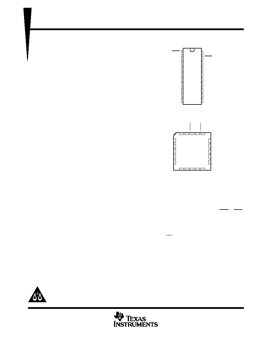
SN54LVC540A . . . J OR W PACKAGE
SN74LVC540A . . . DB, DW, OR PW PACKAGE
(TOP VIEW)
3
2
1 20 19
9 10 11 12 13
4
5
6
7
8
18
17
16
15
14
Y1
Y2
Y3
Y4
Y5
A3
A4
A5
A6
A7
SN54LVC540A . . . FK PACKAGE
(TOP VIEW)
A2
A1
OE1
Y7
Y6
OE2
A8
GND
Y8
V
CC
On products compliant to MIL-PRF-38535, all parameters are tested
unless otherwise noted. On all other products, production
processing does not necessarily include testing of all parameters.
SN54LVC540A, SN74LVC540A
OCTAL BUFFERS/DRIVERS
WITH 3-STATE OUTPUTS
SCAS297H ≠ JANUARY 1993 ≠ REVISED JUNE 1998
2
POST OFFICE BOX 655303
∑
DALLAS, TEXAS 75265
FUNCTION TABLE
INPUTS
OUTPUT
OE1
OE2
A
Y
L
L
L
H
L
L
H
L
H
X
X
Z
X
H
X
Z
logic symbol
2
A1
3
A2
4
A3
1
Y1
18
Y2
17
Y3
16
&
EN
5
A4
6
A5
7
A6
Y4
15
Y5
14
Y6
13
19
OE1
OE2
8
A7
9
A8
Y7
12
Y8
11
This symbol is in accordance with ANSI/IEEE Std 91-1984 and IEC Publication 617-12.
1
logic diagram (positive logic)
OE1
OE2
To Seven Other Channels
A1
Y1
1
19
2
18
SN54LVC540A, SN74LVC540A
OCTAL BUFFERS/DRIVERS
WITH 3-STATE OUTPUTS
SCAS297H ≠ JANUARY 1993 ≠ REVISED JUNE 1998
3
POST OFFICE BOX 655303
∑
DALLAS, TEXAS 75265
absolute maximum ratings over operating free-air temperature range (unless otherwise noted)
Supply voltage range, V
CC
≠0.5 V to 6.5 V
. . . . . . . . . . . . . . . . . . . . . . . . . . . . . . . . . . . . . . . . . . . . . . . . . . . . . . . . .
Input voltage range, V
I
(see Note 1)
≠0.5 V to 6.5 V
. . . . . . . . . . . . . . . . . . . . . . . . . . . . . . . . . . . . . . . . . . . . . . . . .
Voltage range applied to any output in the high-impedance or power-off state, V
O
(see Note 1)
≠0.5 V to 6.5 V
. . . . . . . . . . . . . . . . . . . . . . . . . . . . . . . . . . . . . . . . . . . . . . . . . . . . . . . . . . . . . . . . . . .
Voltage range applied to any output in the high or low state, V
O
(see Notes 1 and 2)
≠0.5 V to V
CC
+ 0.5 V
. . . . . . . . . . . . . . . . . . . . . . . . . . . . . . . . . . . . . . . . . . . . . . . . . . . . . . .
Input clamp current, I
IK
(V
I
< 0)
≠50 mA
. . . . . . . . . . . . . . . . . . . . . . . . . . . . . . . . . . . . . . . . . . . . . . . . . . . . . . . . . . .
Output clamp current, I
OK
(V
O
< 0)
≠50 mA
. . . . . . . . . . . . . . . . . . . . . . . . . . . . . . . . . . . . . . . . . . . . . . . . . . . . . . . .
Continuous output current, I
O
±
50 mA
. . . . . . . . . . . . . . . . . . . . . . . . . . . . . . . . . . . . . . . . . . . . . . . . . . . . . . . . . . . . .
Continuous current through V
CC
or GND
±
100 mA
. . . . . . . . . . . . . . . . . . . . . . . . . . . . . . . . . . . . . . . . . . . . . . . . . .
Package thermal impedance,
JA
(see Note 3): DB package
115
∞
C/W
. . . . . . . . . . . . . . . . . . . . . . . . . . . . . . . .
DW package
97
∞
C/W
. . . . . . . . . . . . . . . . . . . . . . . . . . . . . . . . .
PW package
128
∞
C/W
. . . . . . . . . . . . . . . . . . . . . . . . . . . . . . . .
Storage temperature range, T
stg
≠65
∞
C to 150
∞
C
. . . . . . . . . . . . . . . . . . . . . . . . . . . . . . . . . . . . . . . . . . . . . . . . . . .
Stresses beyond those listed under "absolute maximum ratings" may cause permanent damage to the device. These are stress ratings only, and
functional operation of the device at these or any other conditions beyond those indicated under "recommended operating conditions" is not
implied. Exposure to absolute-maximum-rated conditions for extended periods may affect device reliability.
NOTES:
1. The input negative-voltage and output voltage ratings may be exceeded if the input and output current ratings are observed.
2. The value of VCC is provided in the recommended operating conditions table.
3. The package thermal impedance is calculated in accordance with JESD 51.
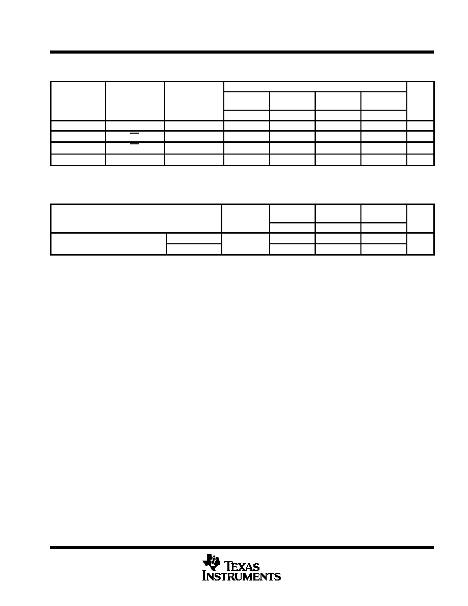
recommended operating conditions (see Note 4)
SN54LVC540A
SN74LVC540A
UNIT
MIN
MAX
MIN
MAX
UNIT
VCC
Supply voltage
Operating
2
3.6
1.65
3.6
V
VCC
Supply voltage
Data retention only
1.5
1.5
V
VCC = 1.65 V to 1.95 V
0.65
◊
VCC
VIH
High-level input voltage
VCC = 2.3 V to 2.7 V
1.7
V
VCC = 2.7 V to 3.6 V
2
2
VCC = 1.65 V to 1.95 V
0.35
◊
VCC
VIL
Low-level input voltage
VCC = 2.3 V to 2.7 V
0.7
V
VCC = 2.7 V to 3.6 V
0.8
0.8
VI
Input voltage
0
5.5
0
5.5
V
VO
Output voltage
High or low state
0
VCC
0
VCC
V
VO
Output voltage
3 state
0
5.5
0
5.5
V
VCC = 1.65 V
≠4
IOH
High level output current
VCC = 2.3 V
≠8
mA
IOH
High-level output current
VCC = 2.7 V
≠12
≠12
mA
VCC = 3 V
≠24
≠24
VCC = 1.65 V
4
IOL
Low level output current
VCC = 2.3 V
8
mA
IOL
Low-level output current
VCC = 2.7 V
12
12
mA
VCC = 3 V
24
24
TA
Operating free-air temperature
≠55
125
≠40
85
∞
C
NOTE 4: All unused inputs of the device must be held at VCC or GND to ensure proper device operation. Refer to the TI application report,
Implications of Slow or Floating CMOS Inputs, literature number SCBA004.
SN54LVC540A, SN74LVC540A
OCTAL BUFFERS/DRIVERS
WITH 3-STATE OUTPUTS
SCAS297H ≠ JANUARY 1993 ≠ REVISED JUNE 1998
4
POST OFFICE BOX 655303
∑
DALLAS, TEXAS 75265
electrical characteristics over recommended operating free-air temperature range (unless
otherwise noted)
PARAMETER
TEST CONDITIONS
V
SN54LVC540A
SN74LVC540A
UNIT
PARAMETER
TEST CONDITIONS
VCC
MIN
TYP
MAX
MIN
TYP
MAX
UNIT
IOH = 100
µ
A
1.65 V to 3.6 V
VCC≠0.2
IOH = ≠100
µ
A
2.7 V to 3.6 V
VCC≠0.2
IOH = ≠4 mA
1.65 V
1.2
VOH
IOH = ≠8 mA
2.3 V
1.7
V
IOH = 12 mA
2.7 V
2.2
2.2
IOH = ≠12 mA
3 V
2.4
2.4
IOH = ≠24 mA
3 V
2.2
2.2
IOL = 100
µ
A
1.65 V to 3.6 V
0.2
IOL = 100
µ
A
2.7 V to 3.6 V
0.2
VOL
IOL = 4 mA
1.65 V
0.45
V
VOL
IOL = 8 mA
2.3 V
0.7
V
IOL = 12 mA
2.7 V
0.4
0.4
IOL = 24 mA
3 V
0.55
0.55
II
VI = 0 to 5.5 V
3.6 V
±
5
±
5
µ
A
Ioff
VI or VO = 5.5 V
0
±
10
µ
A
IOZ
VO = 0 to 5.5 V
3.6 V
±
15
±
10
µ
A
ICC
VI = VCC or GND
IO = 0
3 6 V
10
10
µ
A
ICC
3.6 V
VI
5.5 V
IO = 0
3.6 V
10
10
µ
A
ICC
One input at VCC ≠ 0.6 V,
Other inputs at VCC or GND
2.7 V to 3.6 V
500
500
µ
A
Ci
VI = VCC or GND
3.3 V
4
4
pF
Co
VO = VCC or GND
3.3 V
5.5
5.5
pF
All typical values are at VCC = 3.3 V, TA = 25
∞
C.
This applies in the disabled state only.
switching characteristics over recommended operating free-air temperature range (unless
otherwise noted) (see Figure 3)
SN54LVC540A
PARAMETER
FROM
(INPUT)
TO
(OUTPUT)
VCC = 2.7 V
VCC = 3.3 V
±
0.3 V
UNIT
MIN
MAX
MIN
MAX
tpd
A
Y
7.1
1
5.3
ns
ten
OE
Y
8
1
6.6
ns
tdis
OE
Y
8.2
1
7.4
ns
SN54LVC540A, SN74LVC540A
OCTAL BUFFERS/DRIVERS
WITH 3-STATE OUTPUTS
SCAS297H ≠ JANUARY 1993 ≠ REVISED JUNE 1998
5
POST OFFICE BOX 655303
∑
DALLAS, TEXAS 75265
switching characteristics over recommended operating free-air temperature range (unless
otherwise noted) (see Figures 1 through 3)
SN74LVC540A
PARAMETER
FROM
(INPUT)
TO
(OUTPUT)
VCC = 1.8 V
±
0.15 V
VCC = 2.5 V
±
0.2 V
VCC = 2.7 V
VCC = 3.3 V
±
0.3 V
UNIT
MIN
MAX
MIN
MAX
MIN
MAX
MIN
MAX
tpd
A
Y
7.1
1.4
5.3
ns
ten
OE
Y
8
1.1
6.6
ns
tdis
OE
Y
8.2
1.8
7.4
ns
tsk(o)
1
ns
This information was not available at the time of publication.
Skew between any two outputs of the same package switching in the same direction
operating characteristics, T
A
= 25
∞
C
PARAMETER
TEST
CONDITIONS
VCC = 1.8 V
±
0.15 V
VCC = 2.5 V
±
0.2 V
VCC = 3.3 V
±
0.3 V
UNIT
CONDITIONS
TYP
TYP
TYP
Cpd
Power dissipation capacitance
Outputs enabled
f = 10 MHz
31
pF
Cpd
per buffer/driver
Outputs disabled
f = 10 MHz
3
pF
This information was not available at the time of publication.