SN54LVT16952, SN74LVT16952
3.3-V ABT 16-BIT REGISTERED TRANSCEIVERS
WITH 3-STATE OUTPUTS
SCBS151D ≠ MAY 1992 ≠ REVISED AUGUST 1996
1
POST OFFICE BOX 655303
∑
DALLAS, TEXAS 75265
D
State-of-the-Art Advanced BiCMOS
Technology (ABT) Design for 3.3-V
Operation and Low-Static Power
Dissipation
D
Members of the Texas Instruments
Widebus
TM
Family
D
Support Mixed-Mode Signal Operation (5-V
Input and Output Voltages With 3.3-V V
CC
)
D
Support Unregulated Battery Operation
Down to 2.7 V
D
Typical V
OLP
(Output Ground Bounce)
< 0.8 V at V
CC
= 3.3 V, T
A
= 25
∞
C
D
ESD Protection Exceeds 2000 V Per
MIL-STD-883, Method 3015; Exceeds 200 V
Using Machine Model
(C = 200 pF, R = 0)
D
Latch-Up Performance Exceeds 500 mA
Per JEDEC Standard JESD-17
D
Bus-Hold Data Inputs Eliminate the Need
for External Pullup Resistors
D
Support Live Insertion
D
Distributed V
CC
and GND Pin Configuration
Minimizes High-Speed Switching Noise
D
Flow-Through Architecture Optimizes
PCB Layout
D
Package Options Include Plastic 300-mil
Shrink Small-Outline (DL) and Thin Shrink
Small-Outline (DGG) Packages and 380-mil
Fine-Pitch Ceramic Flat (WD) Package
Using 25-mil Center-to-Center Spacings
description
The 'LVT16952 are 16-bit registered transceivers designed for low-voltage (3.3-V) V
CC
operation, but with the
capability to provide a TTL interface to a 5-V system environment. These devices can be used as two 8-bit
transceivers or one 16-bit transceiver. Data on the A or B bus is stored in the registers on the low-to-high
transition of the clock (CLKAB or CLKBA) input provided that the clock-enable (CLKENAB or CLKENBA) input
is low. Taking the output-enable (OEAB or OEBA) input low accesses the data on either port.
Active bus-hold circuitry is provided to hold unused or floating data inputs at a valid logic level.
To ensure the high-impedance state during power up or power down, OE should be tied to V
CC
through a pullup
resistor; the minimum value of the resistor is determined by the current-sinking capability of the driver.
The SN74LVT16952 is available in TI's shrink small-outline (DL) and thin shrink small-outline (DGG) packages,
which provide twice the I/O pin count and functionality of standard small-outline packages in the same
printed-circuit-board area.
Copyright
©
1996, Texas Instruments Incorporated
PRODUCTION DATA information is current as of publication date.
Products conform to specifications per the terms of Texas Instruments
standard warranty. Production processing does not necessarily include
testing of all parameters.
Widebus is a trademark of Texas Instruments Incorporated.
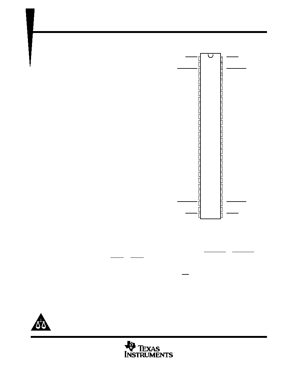
1OEBA
1CLKBA
1CLKENBA
GND
1B1
1B2
V
CC
1B3
1B4
1B5
GND
1B6
1B7
1B8
2B1
2B2
2B3
GND
2B4
2B5
2B6
V
CC
2B7
2B8
GND
2CLKENBA
2CLKBA
2OEBA
1
2
3
4
5
6
7
8
9
10
11
12
13
14
15
16
17
18
19
20
21
22
23
24
25
26
27
28
56
55
54
53
52
51
50
49
48
47
46
45
44
43
42
41
40
39
38
37
36
35
34
33
32
31
30
29
1OEAB
1CLKAB
1CLKENAB
GND
1A1
1A2
V
CC
1A3
1A4
1A5
GND
1A6
1A7
1A8
2A1
2A2
2A3
GND
2A4
2A5
2A6
V
CC
2A7
2A8
GND
2CLKENAB
2CLKAB
2OEAB
SN54LVT16952 . . . WD PACKAGE
SN74LVT16952 . . . DGG OR DL PACKAGE
(TOP VIEW)
Please be aware that an important notice concerning availability, standard warranty, and use in critical applications of
Texas Instruments semiconductor products and disclaimers thereto appears at the end of this data sheet.
SN54LVT16952, SN74LVT16952
3.3-V ABT 16-BIT REGISTERED TRANSCEIVERS
WITH 3-STATE OUTPUTS
SCBS151D ≠ MAY 1992 ≠ REVISED AUGUST 1996
2
POST OFFICE BOX 655303
∑
DALLAS, TEXAS 75265
description (continued)
The SN54LVT16952 is characterized for operation over the full military temperature range of ≠55
∞
C to 125
∞
C.
The SN74LVT16952 is characterized for operation from ≠40
∞
C to 85
∞
C.
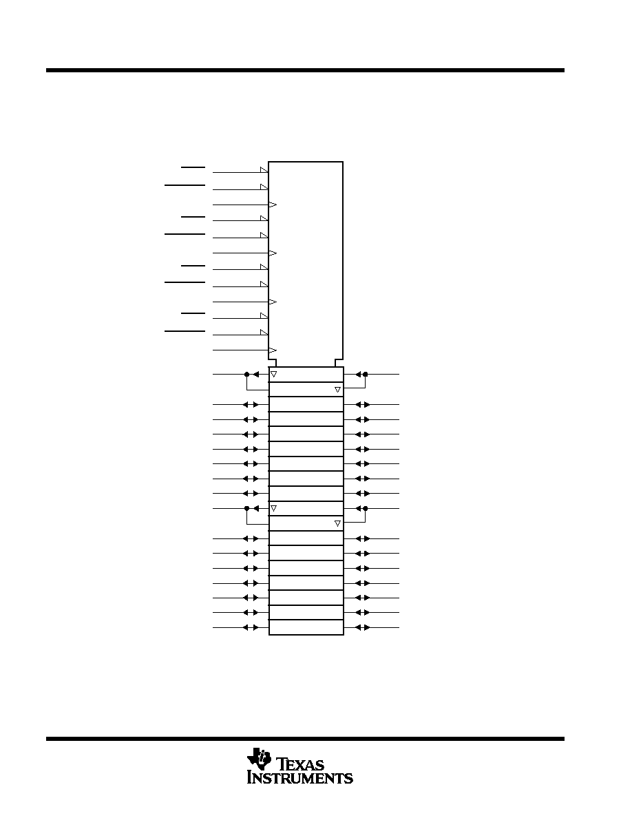
logic symbol
1OEBA
1CLKENBA
1OEAB
1CLKENAB
2OEBA
2CLKENBA
2OEAB
2CLKENAB
G8
26
27
2CLKAB
8C12
1A1
5
6D
1A2
6
1A3
8
1A4
9
1A5
10
1A6
12
1A7
13
1A8
14
1B1
52
5D
1B6
45
1B7
44
1B8
43
1B2
51
1B3
49
1B4
48
1B5
47
EN10
28
G7
31
30
2CLKBA
7C11
EN9
29
G2
3
2
1CLKAB
2C6
EN4
1
G1
54
55
1CLKBA
1C5
EN3
56
3
4
2A1
15
12D
2A2
16
2A3
17
2A4
19
2A5
20
2A6
21
2A7
23
2A8
24
2B1
42
11D
2B6
36
2B7
34
2B8
33
2B2
41
2B3
40
2B4
38
2B5
37
9
10
This symbol is in accordance with ANSI/IEEE Std 91-1984 and IEC Publication 617-12.
SN54LVT16952, SN74LVT16952
3.3-V ABT 16-BIT REGISTERED TRANSCEIVERS
WITH 3-STATE OUTPUTS
SCBS151D ≠ MAY 1992 ≠ REVISED AUGUST 1996
3
POST OFFICE BOX 655303
∑
DALLAS, TEXAS 75265
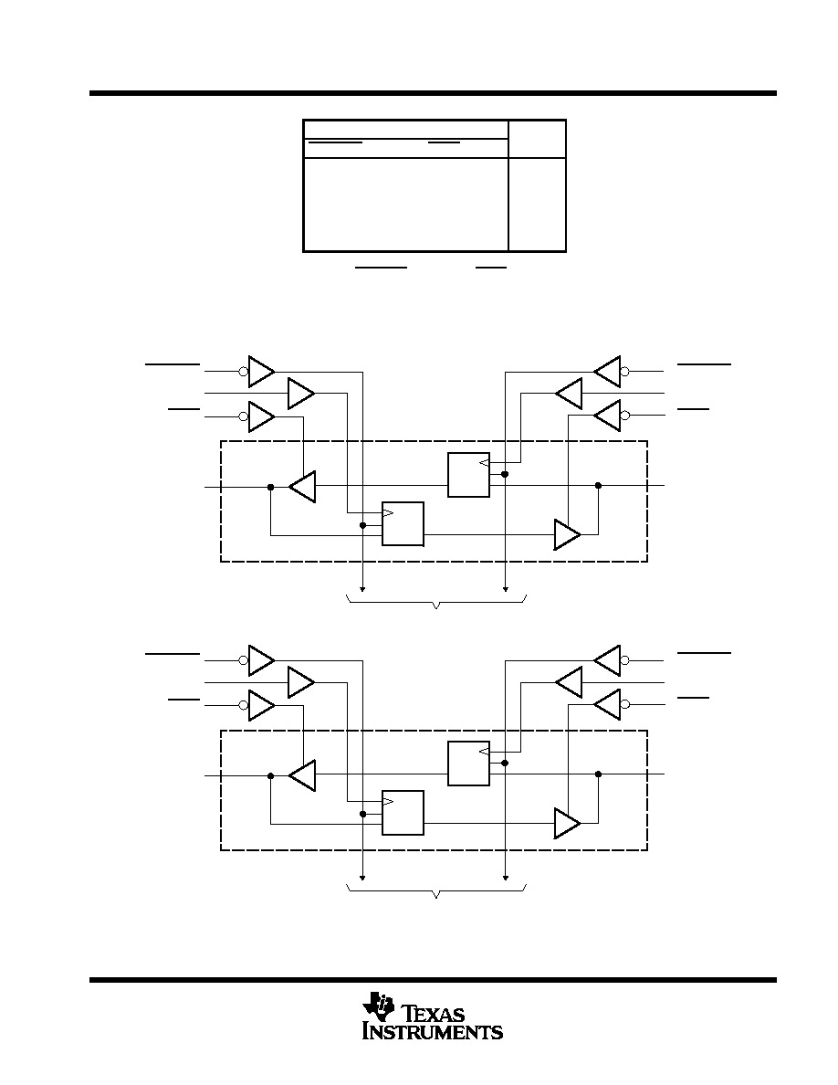
FUNCTION TABLE
INPUTS
OUTPUT
CLKENAB
CLKAB
OEAB
A
B
H
X
L
X
B0
X
L
L
X
B0
L
L
L
L
L
L
H
H
X
X
H
X
Z
A-to-B data flow is shown; B-to-A data flow is similar
but uses CLKENBA, CLKBA, and OEBA.
Level of B before the indicated steady-state input
conditions were established
logic diagram (positive logic)
52
5
2
1
54
55
56
3
To Seven Other Channels
42
26
27
28
31
30
29
15
C1
1D
C1
1D
1CLKAB
1CLKBA
1OEBA
1OEAB
1A1
1B1
One of Eight
Channels
CE
CE
1CLKENAB
1CLKENBA
To Seven Other Channels
C1
1D
C1
1D
2CLKAB
2CLKBA
2OEBA
2OEAB
2A1
2B1
One of Eight
Channels
CE
CE
2CLKENAB
2CLKENBA
SN54LVT16952, SN74LVT16952
3.3-V ABT 16-BIT REGISTERED TRANSCEIVERS
WITH 3-STATE OUTPUTS
SCBS151D ≠ MAY 1992 ≠ REVISED AUGUST 1996
4
POST OFFICE BOX 655303
∑
DALLAS, TEXAS 75265
absolute maximum ratings over operating free-air temperature range (unless otherwise noted)
Supply voltage range, V
CC
≠0.5 V to 4.6 V
. . . . . . . . . . . . . . . . . . . . . . . . . . . . . . . . . . . . . . . . . . . . . . . . . . . . . . . . .
Input voltage range, V
I
(see Note 1)
≠0.5 V to 7 V
. . . . . . . . . . . . . . . . . . . . . . . . . . . . . . . . . . . . . . . . . . . . . . . . . .
Voltage range applied to any output in the high state or power-off state, V
O
(see Note 1)
≠0.5 V to 7 V
. . . .
Current into any output in the low state, I
O
: SN54LVT16952 96
mA
. . . . . . . . . . . . . . . . . . . . . . . . . . . . . . . . . . .
SN74LVT16952 128
mA
. . . . . . . . . . . . . . . . . . . . . . . . . . . . . . . . . .
Current into any output in the high state, I
O
(see Note 2): SN54LVT16952
48 mA
. . . . . . . . . . . . . . . . . . . . . . .
SN74LVT16952 64
mA
. . . . . . . . . . . . . . . . . . . . . . .
Input clamp current, I
IK
(V
I
< 0)
≠50 mA
. . . . . . . . . . . . . . . . . . . . . . . . . . . . . . . . . . . . . . . . . . . . . . . . . . . . . . . . . . .
Output clamp current, I
OK
(V
O
< 0)
≠50 mA
. . . . . . . . . . . . . . . . . . . . . . . . . . . . . . . . . . . . . . . . . . . . . . . . . . . . . . . .
Maximum power dissipation at T
A
= 55
∞
C (in still air) (see Note 3): DGG package
1 W
. . . . . . . . . . . . . . . . . . .
DL package
1.4 W
. . . . . . . . . . . . . . . . . . .
Storage temperature range, T
stg
≠65
∞
C to 150
∞
C
. . . . . . . . . . . . . . . . . . . . . . . . . . . . . . . . . . . . . . . . . . . . . . . . . . .
Stresses beyond those listed under "absolute maximum ratings" may cause permanent damage to the device. These are stress ratings only, and
functional operation of the device at these or any other conditions beyond those indicated under "recommended operating conditions" is not
implied. Exposure to absolute-maximum-rated conditions for extended periods may affect device reliability.
NOTES:
1. The input and output negative-voltage ratings may be exceeded if the input and output clamp-current ratings are observed.
2. This current flows only when the output is in the high state and VO > VCC.
3. The maximum package power dissipation is calculated using a junction temperature of 150
∞
C and a board trace length of 750 mils.
For more information, refer to the
Package Thermal Considerations application note in the ABT Advanced BiCMOS Technology Data
Book.
recommended operating conditions (see Note 4)
SN54LVT16952
SN74LVT16952
UNIT
MIN
MAX
MIN
MAX
UNIT
VCC
Supply voltage
2.7
3.6
2.7
3.6
V
VIH
High-level input voltage
2
2
V
VIL
Low-level input voltage
0.8
0.8
V
VI
Input voltage
5.5
5.5
V
IOH
High-level output current
≠24
≠32
mA
IOL
Low-level output current
48
64
mA
t/
v
Input transition rise or fall rate
Outputs enabled
10
10
ns/V
TA
Operating free-air temperature
≠55
125
≠40
85
∞
C
NOTE 4: Unused control inputs must be held high or low to prevent them from floating.
SN54LVT16952, SN74LVT16952
3.3-V ABT 16-BIT REGISTERED TRANSCEIVERS
WITH 3-STATE OUTPUTS
SCBS151D ≠ MAY 1992 ≠ REVISED AUGUST 1996
5
POST OFFICE BOX 655303
∑
DALLAS, TEXAS 75265
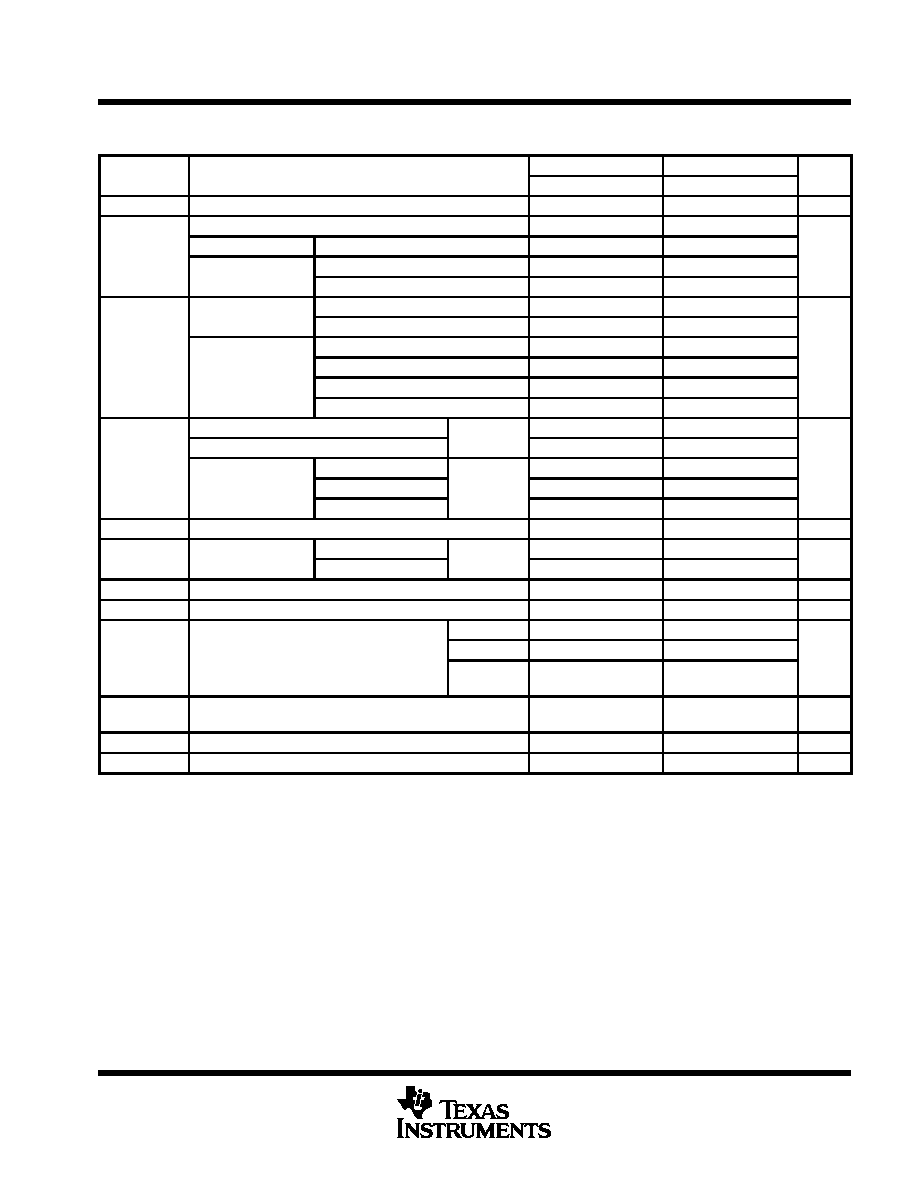
electrical characteristics over recommended operating free-air temperature range (unless
otherwise noted)
PARAMETER
TEST CONDITIONS
SN54LVT16952
SN74LVT16952
UNIT
PARAMETER
TEST CONDITIONS
MIN
TYP
MAX
MIN
TYP
MAX
UNIT
VIK
VCC = 2.7 V,
II = ≠18 mA
≠1.2
≠1.2
V
VCC = MIN to MAX, IOH = ≠100
µ
A
VCC≠0.2
VCC≠0.2
VOH
VCC = 2.7 V,
IOH = ≠8 mA
2.4
2.4
V
VOH
VCC = 3 V
IOH = ≠24 mA
2
V
VCC = 3 V
IOH = ≠32 mA
2
VCC = 2 7 V
IOL = 100
µ
A
0.2
0.2
VCC = 2.7 V
IOL = 24 mA
0.5
0.5
VOL
IOL = 16 mA
0.4
0.4
V
VOL
VCC = 3 V
IOL = 32 mA
0.5
0.5
V
VCC = 3 V
IOL = 48 mA
0.55
IOL = 64 mA
0.55
VCC = 3.6 V,
VI = VCC or GND
Control
±
1
±
1
VCC = 0 or MAX,
VI = 5.5 V
inputs
10
10
II
VI = 5.5 V
ß
100
20
µ
A
VCC = 3.6 V
VI = VCC
A or B portsß
1
1
VI = 0
≠5
≠5
Ioff
VCC = 0,
VI or VO = 0 to 4.5 V
±
100
µ
A
II(h ld)
VCC = 3 V
VI = 0.8 V
A or B ports
75
75
µ
A
II(hold)
VCC = 3 V
VI = 2 V
A or B ports
≠75
≠75
µ
A
IOZH
VCC = 3.6 V,
VO = 3 V
1
1
µ
A
IOZL
VCC = 3.6 V,
VO = 0.5 V
≠1
≠1
µ
A
Outputs high
0.12
0.12
ICC
VCC = 3.6 V, IO = 0,
Outputs low
5
5
mA
ICC
VI = VCC or GND
Outputs
disabled
0.12
0.12
mA
ICC∂
VCC = 3 V to 3.6 V, One input at VCC ≠ 0.6 V,
Other inputs at VCC or GND
0.2
0.2
mA
Ci
VI = 3 V or 0
4
4
pF
Cio
VO = 3 V or 0
13
13
pF
All typical values are at VCC = 3.3 V, TA = 25
∞
C.
For conditions shown as MIN or MAX, use the appropriate value specified under recommended operating conditions.
ß Unused pins at VCC or GND
∂ This is the increase in supply current for each input that is at the specified TTL voltage level rather than VCC or GND.