SN54HC14, SN74HC14
HEX SCHMITT TRIGGER INVERTERS
SCLS085E - DECEMBER 1982 - REVISED NOVEMBER 2004
1
POST OFFICE BOX 655303
∑
DALLAS, TEXAS 75265
D
Wide Operating Voltage Range of 2 V to 6 V
D
Outputs Can Drive Up To 10 LSTTL Loads
D
Low Power Consumption, 20-
µ
A Max I
CC
D
Typical t
pd
= 11 ns
D
±
4-mA Output Drive at 5 V
D
Low Input Current of 1
µ
A Max
1
2
3
4
5
6
7
14
13
12
11
10
9
8
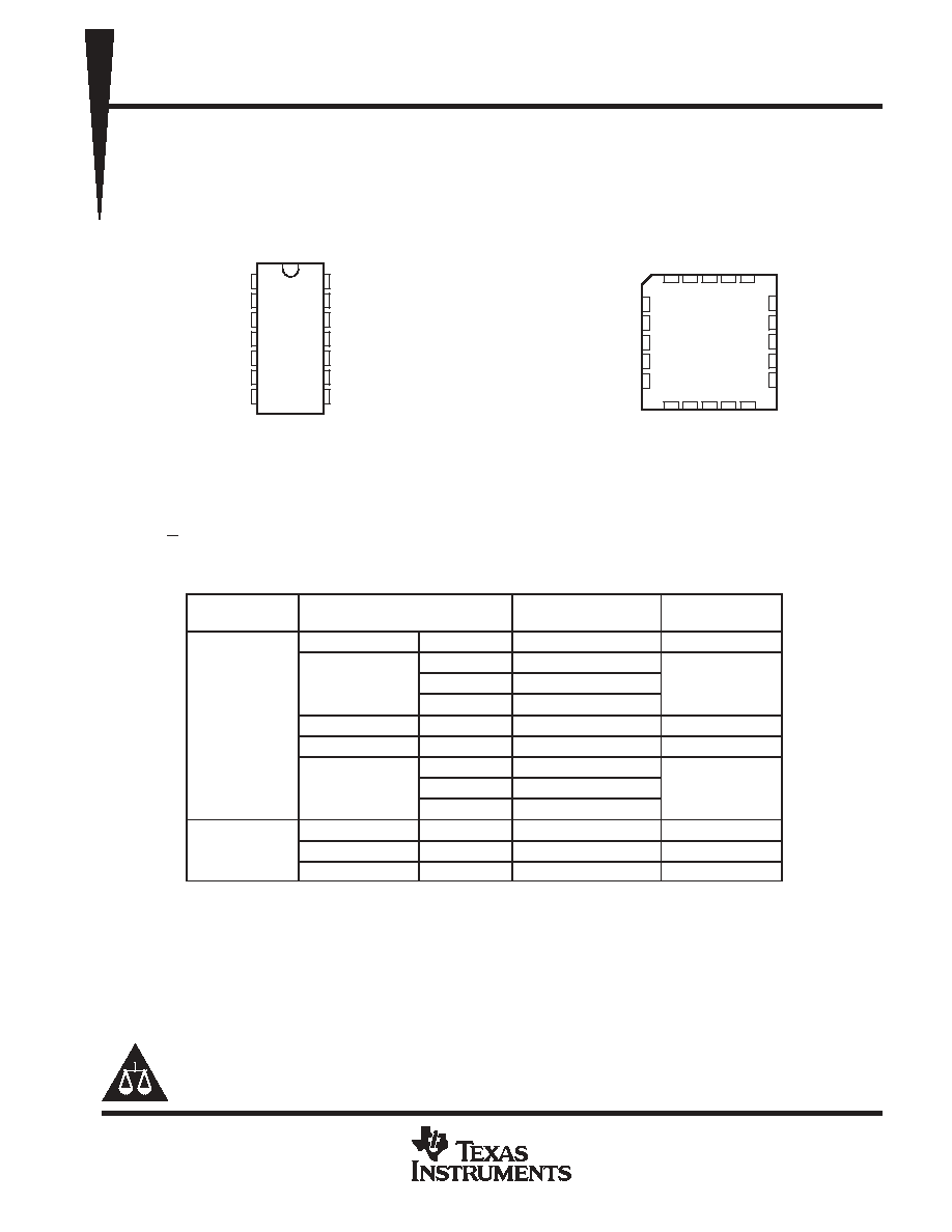
1A
1Y
2A
2Y
3A
3Y
GND
V
CC
6A
6Y
5A
5Y
4A
4Y
SN54HC14 . . . J OR W PACKAGE
SN74HC14 . . . D, DB, N, NS, OR PW PACKAGE
(TOP VIEW)
3
2 1 20 19
9 10 11 12 13
4
5
6
7
8
18
17
16
15
14
6Y
NC
5A
NC
5Y
2A
NC
2Y
NC
3A
1Y
1A
NC
4Y
4A
V
6A
3Y
GND
NC
SN54HC14 . . . FK PACKAGE
(TOP VIEW)
CC
NC - No internal connection
description/ordering information
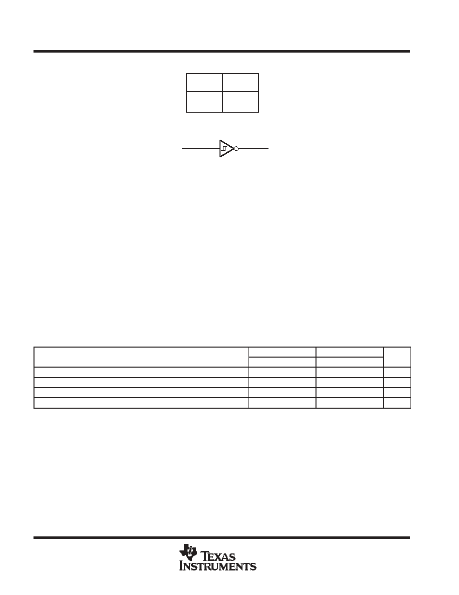
These Schmitt-trigger devices contain six independent inverters. They perform the Boolean function
Y = A in positive logic.
ORDERING INFORMATION
TA
PACKAGE
ORDERABLE
PART NUMBER
TOP-SIDE
MARKING
PDIP - N
Tube of 25
SN74HC14N
SN74HC14N
Tube of 50
SN74HC14D
SOIC - D
Reel of 2500
SN74HC14DR
HC14
SOIC - D
Reel of 250
SN74HC14DT
HC14
-40
∞
C to 85
∞
C
SOP - NS
Reel of 2000
SN74HC14NSR
HC14
-40 C to 85 C
SSOP - DB
Reel of 2000
SN74HC14DBR
HC14
Tube of 90
SN74HC14PW
TSSOP - PW
Reel of 2000
SN74HC14PWR
HC14
TSSOP - PW
Reel of 250
SN74HC14PWT
HC14
CDIP - J
Tube
SNJ54HC14J
SNJ54HC14J
-55
∞
C to 125
∞
C
CFP - W
Tube
SNJ54HC14W
SNJ54HC14W
-55 C to 125 C
LCCC - FK
Tube
SNJ54HC14FK
SNJ54HC14FK
Package drawings, standard packing quantities, thermal data, symbolization, and PCB design guidelines are
available at www.ti.com/sc/package.
Please be aware that an important notice concerning availability, standard warranty, and use in critical applications of
Texas Instruments semiconductor products and disclaimers thereto appears at the end of this data sheet.
Copyright
2004, Texas Instruments Incorporated
PRODUCTION DATA information is current as of publication date.
Products conform to specifications per the terms of Texas Instruments
standard warranty. Production processing does not necessarily include
testing of all parameters.
On products compliant to MIL PRF 38535, all parameters are tested
unless otherwise noted. On all other products, production
processing does not necessarily include testing of all parameters.
SN54HC14, SN74HC14
HEX SCHMITT TRIGGER INVERTERS
SCLS085E - DECEMBER 1982 - REVISED NOVEMBER 2004
2
POST OFFICE BOX 655303
∑
DALLAS, TEXAS 75265
FUNCTION TABLE
(each inverter)
INPUT
A
OUTPUT
Y
H
L
L
H
logic diagram (positive logic)
A
Y
absolute maximum ratings over operating free-air temperature range (unless otherwise noted)
Supply voltage range, V
CC
-0.5 V to 7 V
. . . . . . . . . . . . . . . . . . . . . . . . . . . . . . . . . . . . . . . . . . . . . . . . . . . . . . . . . .
Input clamp current, I
IK
(V
I
< 0 or V
I
> V
CC
) (see Note 1)
±
20 mA
. . . . . . . . . . . . . . . . . . . . . . . . . . . . . . . . . . . .
Output clamp current, I
OK
(V
O
< 0 or V
O
> V
CC
) (see Note 1)
±
20 mA
. . . . . . . . . . . . . . . . . . . . . . . . . . . . . . . .
Continuous output current, I
O
(V
O
= 0 to V
CC
)
±
25 mA
. . . . . . . . . . . . . . . . . . . . . . . . . . . . . . . . . . . . . . . . . . . . . .
Continuous current through V
CC
or GND
±
50 mA
. . . . . . . . . . . . . . . . . . . . . . . . . . . . . . . . . . . . . . . . . . . . . . . . . . .
Package thermal impedance,
JA
(see Note 2): D package
86
∞
C/W
. . . . . . . . . . . . . . . . . . . . . . . . . . . . . . . . . . .
DB package
96
∞
C/W
. . . . . . . . . . . . . . . . . . . . . . . . . . . . . . . . .
N package
80
∞
C/W
. . . . . . . . . . . . . . . . . . . . . . . . . . . . . . . . . . .
NS package
76
∞
C/W
. . . . . . . . . . . . . . . . . . . . . . . . . . . . . . . . .
PW package
113
∞
C/W
. . . . . . . . . . . . . . . . . . . . . . . . . . . . . . . .
Storage temperature range, T
stg
-65
∞
C to 150
∞
C
. . . . . . . . . . . . . . . . . . . . . . . . . . . . . . . . . . . . . . . . . . . . . . . . . . .
Stresses beyond those listed under "absolute maximum ratings" may cause permanent damage to the device. These are stress ratings only, and
functional operation of the device at these or any other conditions beyond those indicated under "recommended operating conditions" is not
implied. Exposure to absolute-maximum-rated conditions for extended periods may affect device reliability.
NOTES:
1. The input and output voltage ratings may be exceeded if the input and output current ratings are observed.
2. The package thermal impedance is calculated in accordance with JESD 51-7.
recommended operating conditions (see Note 3)
SN54HC14
SN74HC14
UNIT
MIN
NOM
MAX
MIN
NOM
MAX
UNIT
VCC
Supply voltage
2
5
6
2
5
6
V
VI
Input voltage
0
VCC
0
VCC
V
VO
Output voltage
0
VCC
0
VCC
V
TA
Operating free-air temperature
-55
125
-40
85
∞
C
NOTE 3: All unused inputs of the device must be held at VCC or GND to ensure proper device operation. Refer to the TI application report,
Implications of Slow or Floating CMOS Inputs, literature number SCBA004.
SN54HC14, SN74HC14
HEX SCHMITT TRIGGER INVERTERS
SCLS085E - DECEMBER 1982 - REVISED NOVEMBER 2004
3
POST OFFICE BOX 655303
∑
DALLAS, TEXAS 75265
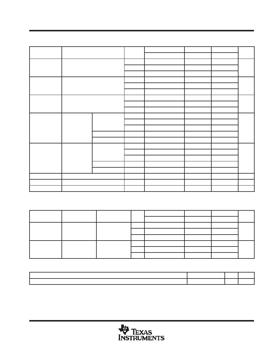
electrical characteristics over recommended operating free-air temperature range (unless
otherwise noted)
PARAMETER
TEST CONDITIONS
VCC
TA = 25
∞
C
SN54HC14
SN74HC14
UNIT
PARAMETER
TEST CONDITIONS
VCC
MIN
TYP
MAX
MIN
MAX
MIN
MAX
UNIT
2 V
0.7
1.2
1.5
0.7
1.5
0.7
1.5
VT+
4.5 V
1.55
2.5
3.15
1.55
3.15
1.55
3.15
V
VT+
6 V
2.1
3.3
4.2
2.1
4.2
2.1
4.2
V
2 V
0.3
0.6
1
0.3
1
0.3
1
VT-
4.5 V
0.9
1.6
2.45
0.9
2.45
0.9
2.45
V
VT-
6 V
1.2
2
3.2
1.2
3.2
1.2
3.2
V
2 V
0.2
0.6
1.2
0.2
1.2
0.2
1.2
VT+ - VT-
4.5 V
0.4
0.9
2.1
0.4
2.1
0.4
2.1
V
VT+ - VT-
6 V
0.5
1.3
2.5
0.5
2.5
0.5
2.5
V
2 V
1.9
1.998
1.9
1.9
IOH = -20
µ
A
4.5 V
4.4
4.499
4.4
4.4
VOH
VI = VIH or VIL
IOH = -20
µ
A
6 V
5.9
5.999
5.9
5.9
V
VOH
VI = VIH or VIL
IOH = -4 mA
4.5 V
3.98
4.3
3.7
3.84
V
IOH = -5.2 mA
6 V
5.48
5.8
5.2
5.34
2 V
0.002
0.1
0.1
0.1
IOL = 20
µ
A
4.5 V
0.001
0.1
0.1
0.1
VOL
VI = VIH or VIL
IOL = 20
µ
A
6 V
0.001
0.1
0.1
0.1
V
VOL
VI = VIH or VIL
IOL = 4 mA
4.5 V
0.17
0.26
0.4
0.33
V
IOL = 5.2 mA
6 V
0.15
0.26
0.4
0.33
II
VI = VCC or 0
6 V
±
0.1
±
100
±
1000
±
1000
nA
ICC
VI = VCC or 0,
IO = 0
6 V
2
40
20
µ
A
Ci
2 V to 6 V
3
10
10
10
pF
switching characteristics over recommended operating free-air temperature range, C
L
= 50 pF
(unless otherwise noted) (see Figure 1)
PARAMETER
FROM
TO
VCC
TA = 25
∞
C
SN54HC14
SN74HC14
UNIT
PARAMETER
FROM
(INPUT)
TO
(OUTPUT)
VCC
MIN
TYP
MAX
MIN
MAX
MIN
MAX
UNIT
2 V
55
125
190
155
tpd
A
Y
4.5 V
12
25
38
31
ns
tpd
A
Y
6 V
11
21
32
26
ns
2 V
38
75
110
95
tt
Y
4.5 V
8
15
22
19
ns
tt
Y
6 V
6
13
19
16
ns
operating characteristics, T
A
= 25
∞
C
PARAMETER
TEST CONDITIONS
TYP
UNIT
Cpd
Power dissipation capacitance per inverter
No load
20
pF
SN54HC14, SN74HC14
HEX SCHMITT TRIGGER INVERTERS
SCLS085E - DECEMBER 1982 - REVISED NOVEMBER 2004
4
POST OFFICE BOX 655303
∑
DALLAS, TEXAS 75265
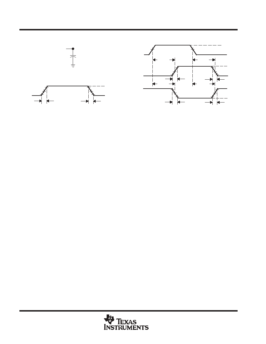
PARAMETER MEASUREMENT INFORMATION
VOLTAGE WAVEFORM
INPUT RISE AND FALL TIMES
50%
50%
10%
10%
90%
90%
VCC
0 V
tr
tf
Input
VOLTAGE WAVEFORMS
PROPAGATION DELAY AND OUTPUT TRANSITION TIMES
50%
50%
50%
10%
10%
90%
90%
VCC
VOH
VOL
0 V
tr
tf
Input
In-Phase
Output
50%
tPLH
tPHL
50%
50%
10%
10%
90%
90%
VOH
VOL
tr
tf
tPHL
tPLH
Out-of-Phase
Output
Test
Point
From Output
Under Test
CL = 50 pF
(see Note A)
LOAD CIRCUIT
NOTES: A. CL includes probe and test-fixture capacitance.
B. Phase relationships between waveforms were chosen arbitrarily. All input pulses are supplied by generators having the following
characteristics: PRR
1 MHz, ZO = 50
, tr = 6 ns, tf = 6 ns.
C. The outputs are measured one at a time, with one input transition per measurement.
D. tPLH and tPHL are the same as tpd.
Figure 1. Load Circuit and Voltage Waveforms
PACKAGING INFORMATION
Orderable Device
Status
(1)
Package
Type
Package
Drawing
Pins Package
Qty
Eco Plan
(2)
Lead/Ball Finish
MSL Peak Temp
(3)
5962-8409101VCA
ACTIVE
CDIP
J
14
1
None
Call TI
Level-NC-NC-NC
5962-8409101VDA
ACTIVE
CFP
W
14
1
None
Call TI
Level-NC-NC-NC
84091012A
ACTIVE
LCCC
FK
20
1
None
Call TI
Level-NC-NC-NC
8409101CA
ACTIVE
CDIP
J
14
1
None
Call TI
Level-NC-NC-NC
8409101DA
ACTIVE
CFP
W
14
1
None
Call TI
Level-NC-NC-NC
JM38510/65702BCA
ACTIVE
CDIP
J
14
1
None
Call TI
Level-NC-NC-NC
JM38510/65702BDA
ACTIVE
CFP
W
14
1
None
Call TI
Level-NC-NC-NC
SN54HC14J
ACTIVE
CDIP
J
14
1
None
Call TI
Level-NC-NC-NC
SN74HC14D
ACTIVE
SOIC
D
14
50
Pb-Free
(RoHS)
CU NIPDAU
Level-2-260C-1 YEAR/
Level-1-235C-UNLIM
SN74HC14DBR
ACTIVE
SSOP
DB
14
2000
Pb-Free
(RoHS)
CU NIPDAU
Level-2-260C-1 YEAR/
Level-1-235C-UNLIM
SN74HC14DR
ACTIVE
SOIC
D
14
2500 Green (RoHS &
no Sb/Br)
CU NIPDAU
Level-1-260C-UNLIM
SN74HC14DT
ACTIVE
SOIC
D
14
250
Pb-Free
(RoHS)
CU NIPDAU
Level-2-260C-1 YEAR/
Level-1-235C-UNLIM
SN74HC14N
ACTIVE
PDIP
N
14
25
Pb-Free
(RoHS)
CU NIPDAU
Level-NC-NC-NC
SN74HC14N3
OBSOLETE
PDIP
N
14
None
Call TI
Call TI
SN74HC14NS
ACTIVE
SO
NS
14
Pb-Free
(RoHS)
CU NIPDAU
Level-2-260C-1 YEAR/
Level-1-235C-UNLIM
SN74HC14NSLE
OBSOLETE
SO
NS
14
None
Call TI
Call TI
SN74HC14NSR
ACTIVE
SO
NS
14
2000
Pb-Free
(RoHS)
CU NIPDAU
Level-2-260C-1 YEAR/
Level-1-235C-UNLIM
SN74HC14PW
ACTIVE
TSSOP
PW
14
90
Pb-Free
(RoHS)
CU NIPDAU
Level-1-250C-UNLIM
SN74HC14PWLE
OBSOLETE
TSSOP
PW
14
None
Call TI
Call TI
SN74HC14PWR
ACTIVE
TSSOP
PW
14
2000
Pb-Free
(RoHS)
CU NIPDAU
Level-1-250C-UNLIM
SN74HC14PWT
ACTIVE
TSSOP
PW
14
250
Pb-Free
(RoHS)
CU NIPDAU
Level-1-250C-UNLIM
SNJ54HC14FK
ACTIVE
LCCC
FK
20
1
None
Call TI
Level-NC-NC-NC
SNJ54HC14J
ACTIVE
CDIP
J
14
1
None
Call TI
Level-NC-NC-NC
SNJ54HC14W
ACTIVE
CFP
W
14
1
None
Call TI
Level-NC-NC-NC
(1)
The marketing status values are defined as follows:
ACTIVE: Product device recommended for new designs.
LIFEBUY: TI has announced that the device will be discontinued, and a lifetime-buy period is in effect.
NRND: Not recommended for new designs. Device is in production to support existing customers, but TI does not recommend using this part in
a new design.
PREVIEW: Device has been announced but is not in production. Samples may or may not be available.
OBSOLETE: TI has discontinued the production of the device.
(2)
Eco Plan - May not be currently available - please check
http://www.ti.com/productcontent
for the latest availability information and additional
product content details.
None: Not yet available Lead (Pb-Free).
Pb-Free (RoHS): TI's terms "Lead-Free" or "Pb-Free" mean semiconductor products that are compatible with the current RoHS requirements
for all 6 substances, including the requirement that lead not exceed 0.1% by weight in homogeneous materials. Where designed to be soldered
at high temperatures, TI Pb-Free products are suitable for use in specified lead-free processes.
PACKAGE OPTION ADDENDUM
www.ti.com
28-Feb-2005
Addendum-Page 1