www.ti.com
FEATURES
DESCRIPTION/ORDERING INFORMATION
1
2
3
4
5
6
7
8
9
10
11
12
13
14
15
16
17
18
19
20
21
22
23
24
48
47
46
45
44
43
42
41
40
39
38
37
36
35
34
33
32
31
30
29
28
27
26
25
1OE
1Q1
1Q2
GND
1Q3
1Q4
V
CC
1Q5
1Q6
GND
1Q7
1Q8
2Q1
2Q2
GND
2Q3
2Q4
V
CC
2Q5
2Q6
GND
2Q7
2Q8
2OE
1LE
1D1
1D2
GND
1D3
1D4
V
CC
1D5
1D6
GND
1D7
1D8
2D1
2D2
GND
2D3
2D4
V
CC
2D5
2D6
GND
2D7
2D8
2LE
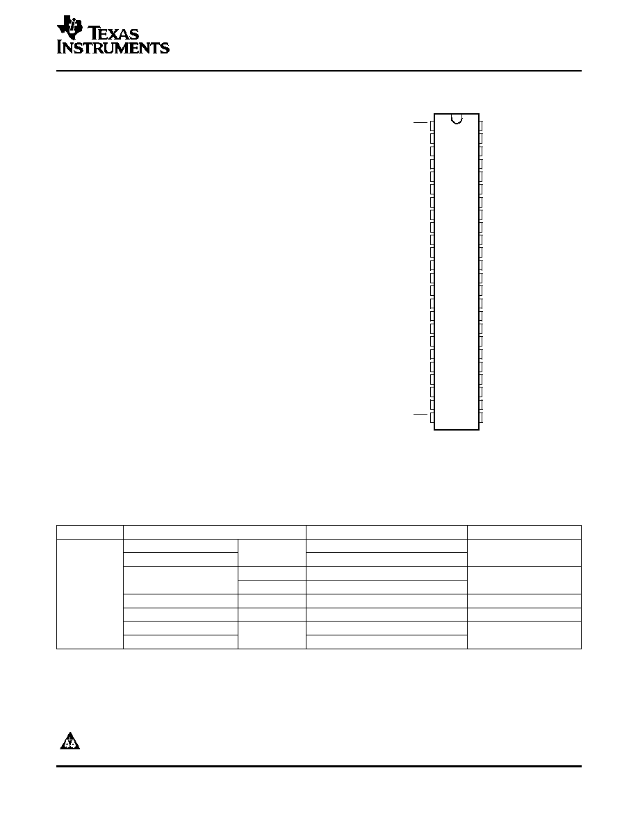
DGG, DGV, OR DL PACKAGE
(TOP VIEW)
SN74LVC16373A
16-BIT TRANSPARENT D-TYPE LATCH
WITH 3-STATE OUTPUTS
SCAS755 ≠ DECEMBER 2003 ≠ REVISED MARCH 2005
∑
Member of the Texas Instruments WidebusTM
Family
∑
Operates From 1.65 V to 3.6 V
∑
Inputs Accept Voltages to 5.5 V
∑
Max t
pd
of 4.2 ns at 3.3 V
∑
Typical V
OLP
(Output Ground Bounce) < 0.8 V
at V
CC
= 3.3 V, T
A
= 25
∞
C
∑
Typical V
OHV
(Output V
OH
Undershoot) > 2 V
at V
CC
= 3.3 V, T
A
= 25
∞
C
∑
I
off
Supports Partial-Power-Down Mode
Operation
∑
Supports Mixed-Mode Signal Operation (5-V
Input and Output Voltages With 3.3-V V
CC
)
∑
Latch-Up Performance Exceeds 100 mA Per
JESD 78, Class II
∑
ESD Protection Exceeds JESD 22
≠ 2000-V Human-Body Model (A114-A)
≠ 1000-V Charged-Device Model (C101)
This 16-bit transparent D-type latch is designed for
1.65-V to 3.6-V V
CC
operation.
The SN74LVC16373A is particularly suitable for
implementing buffer registers, I/O ports, bidirectional
bus drivers, and working registers. The device can be
used as two 8-bit latches or one 16-bit latch. When
the latch-enable (LE) input is high, the Q outputs
follow the data (D) inputs. When LE is taken low, the
Q outputs are latched at the levels set up at the D
inputs.
ORDERING INFORMATION
T
A
PACKAGE
(1)
ORDERABLE PART NUMBER
TOP-SIDE MARKING
FBGA ≠ GRD
SN74LVC16373AGRDR
Tape and reel
LD373A
FBGA ≠ ZRD (Pb-free)
SN74LVC16373AZRDR
Tube
SN74LVC16373ADL
SSOP ≠ DL
LVC16373A
Tape and reel
SN74LVC16373ADLR
≠40
∞
C to 85
∞
C
TSSOP ≠ DGG
Tape and reel
SN74LVC16373ADGGR
LVC16373A
TVSOP ≠ DGV
Tape and reel
SN74LVC16373ADGVR
LD373A
VFBGA ≠ GQL
SN74LVC16373AGQLR
Tape and reel
LD373A
VFBGA ≠ ZQL (Pb-free)
SN74LVC16373AZQLR
(1)
Package drawings, standard packing quantities, thermal data, symbolization, and PCB design guidelines are available at
www.ti.com/sc/package.
Please be aware that an important notice concerning availability, standard warranty, and use in critical applications of Texas
Instruments semiconductor products and disclaimers thereto appears at the end of this data sheet.
Widebus is a trademark of Texas Instruments.
PRODUCTION DATA information is current as of publication date.
Copyright © 2003≠2005, Texas Instruments Incorporated
Products conform to specifications per the terms of the Texas
Instruments standard warranty. Production processing does not
necessarily include testing of all parameters.
www.ti.com
DESCRIPTION/ORDERING INFORMATION (CONTINUED)
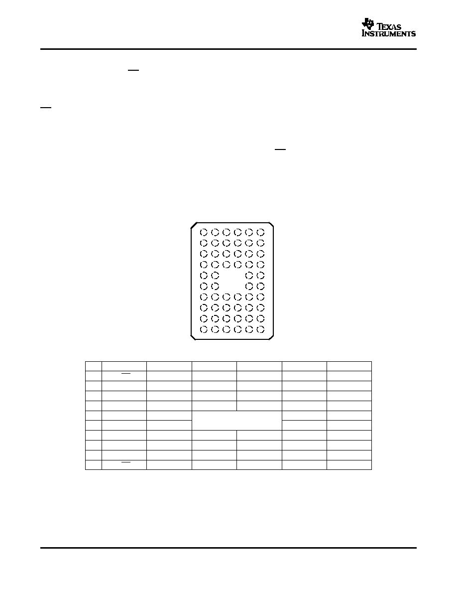
GQL OR ZQL PACKAGE
(TOP VIEW)
A
B
C
D
E
F
G
H
J
K
1
2
3
4
5
6
SN74LVC16373A
16-BIT TRANSPARENT D-TYPE LATCH
WITH 3-STATE OUTPUTS
SCAS755 ≠ DECEMBER 2003 ≠ REVISED MARCH 2005
A buffered output-enable (OE) input can be used to place the eight outputs in either a normal logic state (high or
low logic levels) or the high-impedance state. In the high-impedance state, the outputs neither load nor drive the
bus lines significantly. The high-impedance state and increased drive provide the capability to drive bus lines
without interface or pullup components.
OE does not affect internal operations of the latch. Old data can be retained or new data can be entered while
the outputs are in the high-impedance state.
Inputs can be driven from either 3.3-V or 5-V devices. This feature allows the use of this device as a translator in
a mixed 3.3-V/5-V system environment.
To ensure the high-impedance state during power up or power down, OE should be tied to V
CC
through a pullup
resistor; the minimum value of the resistor is determined by the current-sinking capability of the driver.
This device is fully specified for partial-power-down applications using I
off
. The I
off
circuitry disables the outputs,
preventing damaging current backflow through the device when it is powered down.
TERMINAL ASSIGNMENTS
(1)
1
2
3
4
5
6
A
1OE
NC
NC
NC
NC
1LE
B
1Q2
1Q1
GND
GND
1D1
1D2
C
1Q4
1Q3
V
CC
V
CC
1D3
1D4
D
1Q6
1Q5
GND
GND
1D5
1D6
E
1Q8
1Q7
1D7
1D8
F
2Q1
2Q2
2D2
2D1
G
2Q3
2Q4
GND
GND
2D4
2D3
H
2Q5
2Q6
V
CC
V
CC
2D6
2D5
J
2Q7
2Q8
GND
GND
2D8
2D7
K
2OE
NC
NC
NC
NC
2LE
(1)
NC ≠ No internal connection
2
www.ti.com
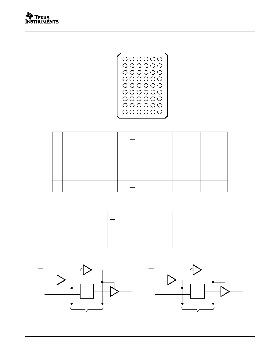
GRD OR ZRD PACKAGE
(TOP VIEW)
J
H
G
F
E
D
C
B
A
2
1
3
4
6
5
1OE
1LE
1D1
To Seven Other Channels
1Q1
C1
1D
1
48
47
2
2OE
2LE
2D1
To Seven Other Channels
2Q1
C1
1D
24
25
36
13
Pin numbers shown are for the DGG, DGV, and DL packages.
SN74LVC16373A
16-BIT TRANSPARENT D-TYPE LATCH
WITH 3-STATE OUTPUTS
SCAS755 ≠ DECEMBER 2003 ≠ REVISED MARCH 2005
TERMINAL ASSIGNMENTS
(1)
1
2
3
4
5
6
A
1Q1
NC
1OE
1LE
NC
1D1
B
1Q3
1Q2
NC
NC
1D2
1D3
C
1Q5
1Q4
V
CC
V
CC
1D4
1D5
D
1Q7
1Q6
GND
GND
1D6
1D7
E
2Q1
1Q8
GND
GND
1D8
2D1
F
2Q3
2Q2
GND
GND
2D2
2D3
G
2Q5
2Q4
V
CC
V
CC
2D4
2D5
H
2Q7
2Q6
NC
NC
2D6
2D7
J
2Q8
NC
2OE
2LE
NC
2D8
(1)
NC ≠ No internal connection
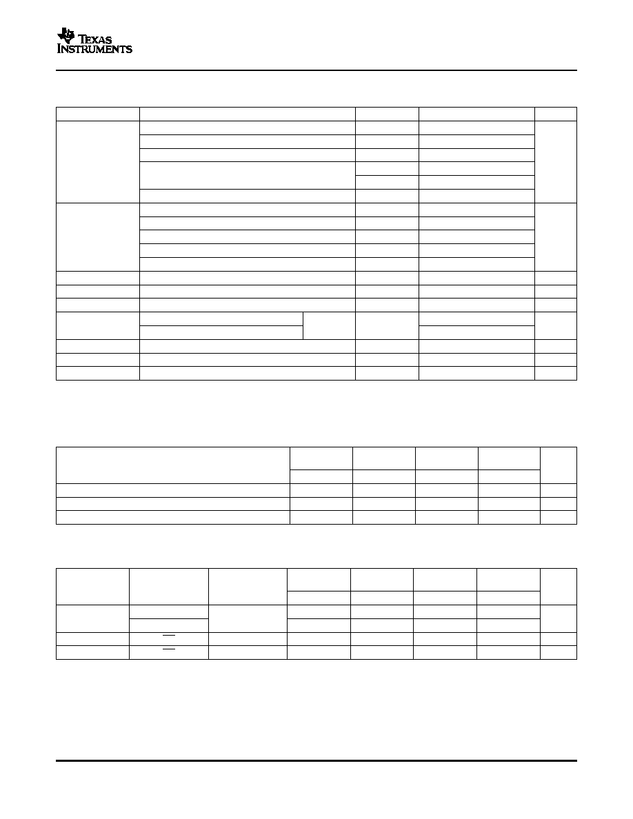
FUNCTION TABLE
INPUTS
OUTPUT
Q
OE
LE
D
L
H
H
H
L
H
L
L
L
L
X
Q
0
H
X
X
Z
LOGIC DIAGRAM (POSITIVE LOGIC)
3
www.ti.com
Absolute Maximum Ratings
(1)
Recommended Operating Conditions
(1)
SN74LVC16373A
16-BIT TRANSPARENT D-TYPE LATCH
WITH 3-STATE OUTPUTS
SCAS755 ≠ DECEMBER 2003 ≠ REVISED MARCH 2005
over operating free-air temperature range (unless otherwise noted)
MIN
MAX
UNIT
V
CC
Supply voltage range
≠0.5
6.5
V
V
I
Input voltage range
(2)
≠0.5
6.5
V
V
O
Voltage range applied to any output in the high-impedance or power-off state
(2)
≠0.5
6.5
V
V
O
Voltage range applied to any output in the high or low state
(2) (3)
≠0.5
V
CC
+ 0.5
V
I
IK
Input clamp current
V
I
< 0
≠50
mA
I
OK
Output clamp current
V
O
< 0
≠50
mA
I
O
Continuous output current
±
50
mA
Continuous current through each V
CC
or GND
±
100
mA
DGG package
70
DGV package
58
JA
Package thermal impedance
(4)
DL package
63
∞
C/W
GQL/ZQL package
42
GRD/ZRD package
36
T
stg
Storage temperature range
≠65
150
∞
C
(1)
Stresses beyond those listed under "absolute maximum ratings" may cause permanent damage to the device. These are stress ratings
only, and functional operation of the device at these or any other conditions beyond those indicated under "recommended operating
conditions" is not implied. Exposure to absolute-maximum-rated conditions for extended periods may affect device reliability.
(2)
The input negative-voltage and output voltage ratings may be exceeded if the input and output current ratings are observed.
(3)
The value of V
CC
is provided in the recommended operating conditions table.
(4)
The package thermal impedance is calculated in accordance with JESD 51-7.
MIN
MAX
UNIT
Operating
1.65
3.6
V
CC
Supply voltage
V
Data retention only
1.5
V
CC
= 1.65 V to 1.95 V
0.65
◊
V
CC
V
IH
High-level input voltage
V
CC
= 2.3 V to 2.7 V
1.7
V
V
CC
= 2.7 V to 3.6 V
2
V
CC
= 1.65 V to 1.95 V
0.35
◊
V
CC
V
IL
Low-level input voltage
V
CC
= 2.3 V to 2.7 V
0.7
V
V
CC
= 2.7 V to 3.6 V
0.8
V
I
Input voltage
0
5.5
V
High or low state
0
V
CC
V
O
Output voltage
V
High-impedance state
0
5.5
V
CC
= 1.65 V
≠4
V
CC
= 2.3 V
≠8
I
OH
High-level output current
mA
V
CC
= 2.7 V
≠12
V
CC
= 3 V
≠24
V
CC
= 1.65 V
4
V
CC
= 2.3 V
8
I
OL
Low-level output current
mA
V
CC
= 2.7 V
12
V
CC
= 3 V
24
t/
v
Input transition rise or fall rate
10
ns/V
T
A
Operating free-air temperature
≠40
85
∞
C
(1)
All unused inputs of the device must be held at V
CC
or GND to ensure proper device operation. Refer to the TI application report,
Implications of Slow or Floating CMOS Inputs, literature number SCBA004.
4
www.ti.com
Electrical Characteristics
Timing Requirements
Switching Characteristics
SN74LVC16373A
16-BIT TRANSPARENT D-TYPE LATCH
WITH 3-STATE OUTPUTS
SCAS755 ≠ DECEMBER 2003 ≠ REVISED MARCH 2005
over recommended operating free-air temperature range (unless otherwise noted)
PARAMETER
TEST CONDITIONS
V
CC
MIN
TYP
(1)
MAX
UNIT
I
OH
= ≠100
µ
A
1.65 V to 3.6 V
V
CC
≠ 0.2
I
OH
= ≠4 mA
1.65 V
1.2
I
OH
= ≠8 mA
2.3 V
1.7
V
OH
V
2.7 V
2.2
I
OH
= ≠12 mA
3 V
2.4
I
OH
= ≠24 mA
3 V
2.2
I
OL
= 100
µ
A
1.65 V to 3.6 V
0.2
I
OL
= 4 mA
1.65 V
0.45
V
OL
I
OL
= 8 mA
2.3 V
0.7
V
I
OL
= 12 mA
2.7 V
0.4
I
OL
= 24 mA
3 V
0.55
I
I
V
I
= 0 to 5.5 V
3.6 V
±
5
µ
A
I
off
V
I
or V
O
= 5.5 V
0
±
10
µ
A
I
OZ
V
O
= 0 to 5.5 V
3.6 V
±
10
µ
A
V
I
= V
CC
or GND
20
I
CC
I
O
= 0
3.6 V
µ
A
3.6 V
V
I
5.5 V
(2)
20
I
CC
One input at V
CC
≠ 0.6 V, Other inputs at V
CC
or GND
2.7 V to 3.6 V
500
µ
A
C
i
V
I
= V
CC
or GND
3.3 V
5
pF
C
o
V
O
= V
CC
or GND
3.3 V
6.5
pF
(1)
All typical values are at V
CC
= 3.3 V, T
A
= 25
∞
C.
(2)
This applies in the disabled state only.
over recommended operating free-air temperature range (unless otherwise noted) (see Figure 1)
V
CC
= 1.8 V
V
CC
= 2.5 V
V
CC
= 3.3 V
V
CC
= 2.7 V
±
0.15 V
±
0.2 V
±
0.3 V
UNIT
MIN
MAX
MIN
MAX
MIN
MAX
MIN
MAX
t
w
Pulse duration, LE high
3.3
3.3
3.3
3.3
ns
t
su
Setup time, data before LE
1.6
1.2
1.7
1.7
ns
t
h
Hold time, data after LE
1
1.1
1.2
1.2
ns
over recommended operating free-air temperature range (unless otherwise noted) (see Figure 1)
V
CC
= 1.8 V
V
CC
= 2.5 V
V
CC
= 3.3 V
V
CC
= 2.7 V
FROM
TO
±
0.15 V
±
0.2 V
±
0.3 V
PARAMETER
UNIT
(INPUT)
(OUTPUT)
MIN
MAX
MIN
MAX
MIN
MAX
MIN
MAX
D
1.5
6.4
1
4.2
1
4.9
1.6
4.2
t
pd
Q
ns
LE
1.5
7.1
1
4.8
1
5.3
2.1
4.6
t
en
OE
Q
1.5
6.7
1
4.7
1
5.7
1.3
4.7
ns
t
dis
OE
Q
1.5
8.4
1
5
1
6.3
2.5
5.9
ns
5