SN74LVC1G66
SINGLE BILATERAL ANALOG SWITCH
SCES323H - JUNE 2001 - REVISED SEPTEMBER 2003
1
POST OFFICE BOX 655303
∑
DALLAS, TEXAS 75265
D
Available in the Texas Instruments
NanoStar
and NanoFree
Packages
D
1.65-V to 5.5-V V
CC
Operation
D
Inputs Accept Voltages to 5.5 V
D
Max t
pd
of 0.8 ns at 3.3 V
D
High On-Off Output Voltage Ratio
D
High Degree of Linearity
D
High Speed, Typically 0.5 ns
(V
CC
= 3 V, C
L
= 50 pF)
D
Low On-State Resistance, Typically
5.5
(V
CC
= 4.5 V)
D
Latch-Up Performance Exceeds 100 mA Per
JESD 78, Class II
D
ESD Protection Exceeds JESD 22
- 2000-V Human-Body Model (A114-A)
- 200-V Machine Model (A115-A)
- 1000-V Charged-Device Model (C101)
description/ordering information
This single analog switch is designed for 1.65-V to 5.5-V V
CC
operation.
The SN74LVC1G66 can handle both analog and digital signals. The device permits signals with amplitudes of
up to 5.5 V (peak) to be transmitted in either direction.
ORDERING INFORMATION
TA
PACKAGE
ORDERABLE
PART NUMBER
TOP-SIDE
MARKING
NanoStar
- WCSP (DSBGA)
0.17-mm Small Bump - YEA
SN74LVC1G66YEAR
-40
∞
C to 85
∞
C
NanoFree
- WCSP (DSBGA)
0.17-mm Small Bump - YZA (Pb-free)
Reel of 3000
SN74LVC1G66YZAR
_ _ _C6_
-40
∞
C to 85
∞
C
NanoStar
- WCSP (DSBGA)
0.23-mm Large Bump - YEP
Reel of 3000
SN74LVC1G66YEPR
_ _ _C6_
NanoFree
- WCSP (DSBGA)
0.23-mm Large Bump - YZP (Pb-free)
SN74LVC1G66YZPR
SOT (SOT-23) - DBV
Reel of 3000
SN74LVC1G66DBVR
C66_
-40
∞
C to 85
∞
C
SOT (SOT-23) - DBV
Reel of 250
SN74LVC1G66DBVT
C66_
-40
∞
C to 85
∞
C
SOT (SC-70) - DCK
Reel of 3000
SN74LVC1G66DCKR
C6_
SOT (SC-70) - DCK
Reel of 250
SN74LVC1G66DCKT
C6_
Package drawings, standard packing quantities, thermal data, symbolization, and PCB design guidelines are available at
www.ti.com/sc/package.
DBV/DCK: The actual top-side marking has one additional character that designates the assembly/test site.
YEA/YZA, YEP/YZP: The actual top-side marking has three preceding characters to denote year, month, and sequence code,
and one following character to designate the assembly/test site. Pin 1 identifier indicates solder-bump composition
(1 = SnPb,
∑
= Pb-free).
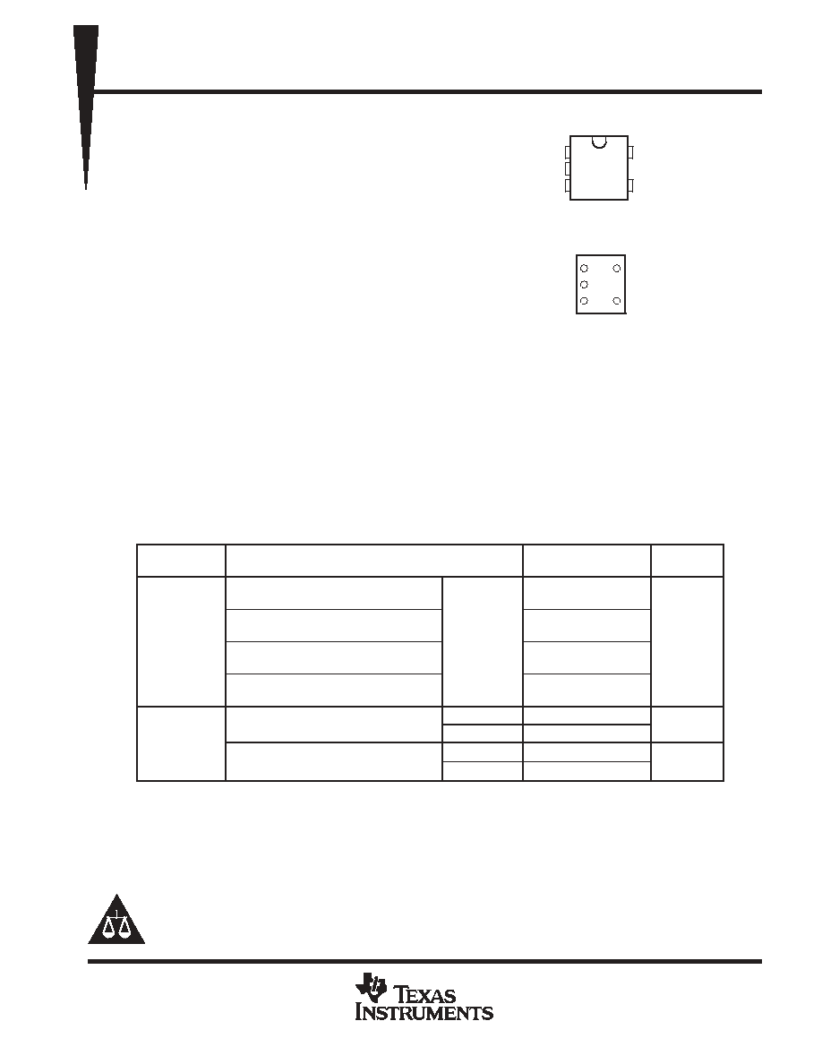
DBV OR DCK PACKAGE
(TOP VIEW)
1
2
3
5
4
A
B
GND
V
CC
C
3
2
1
4
5
GND
B
A
C
V
CC
YEA, YEP, YZA, OR YZP PACKAGE
(BOTTOM VIEW)
Copyright
2003, Texas Instruments Incorporated
Please be aware that an important notice concerning availability, standard warranty, and use in critical applications of
Texas Instruments semiconductor products and disclaimers thereto appears at the end of this data sheet.
NanoStar and NanoFree are trademarks of Texas Instruments.
PRODUCTION DATA information is current as of publication date.
Products conform to specifications per the terms of Texas Instruments
standard warranty. Production processing does not necessarily include
testing of all parameters.
SN74LVC1G66
SINGLE BILATERAL ANALOG SWITCH
SCES323H - JUNE 2001 - REVISED SEPTEMBER 2003
2
POST OFFICE BOX 655303
∑
DALLAS, TEXAS 75265
description/ordering information (continued)
NanoStar
and NanoFree
package technology is a major breakthrough in IC packaging concepts, using the
die as the package.
Applications include signal gating, chopping, modulation or demodulation (modem), and signal multiplexing for
analog-to-digital and digital-to-analog conversion systems.
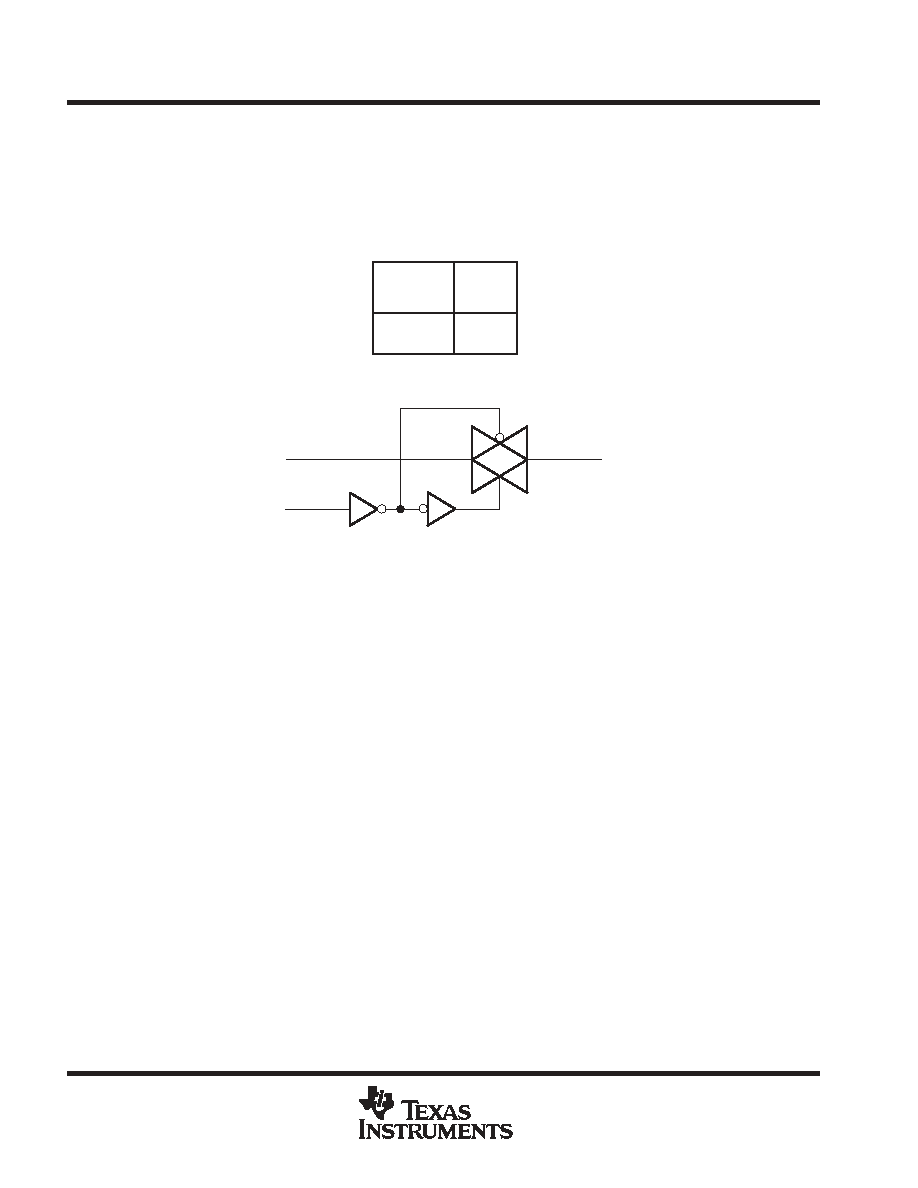
FUNCTION TABLE
CONTROL
INPUT
(C)
SWITCH
L
OFF
H
ON
logic diagram (positive logic)
B
C
A
1
4
2
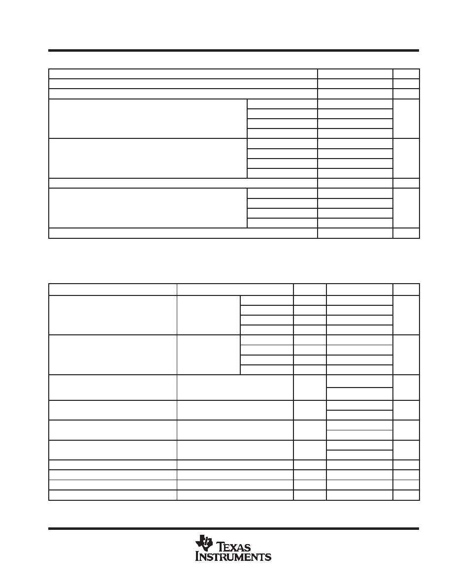
absolute maximum ratings over operating free-air temperature range (unless otherwise noted)
Supply voltage range, V
CC
(see Note 1)
-0.5 V to 6.5 V
. . . . . . . . . . . . . . . . . . . . . . . . . . . . . . . . . . . . . . . . . . . . .
Input voltage range, V
I
(see Notes 1 and 2)
-0.5 V to 6.5 V
. . . . . . . . . . . . . . . . . . . . . . . . . . . . . . . . . . . . . . . . . .
Switch I/O voltage range, V
I/O
(see Notes 1, 2, and 3)
-0.5 V to V
CC
+ 0.5 V
. . . . . . . . . . . . . . . . . . . . . . . . . . .
Control input clamp current, I
IK
(V
I
< 0)
-50 mA
. . . . . . . . . . . . . . . . . . . . . . . . . . . . . . . . . . . . . . . . . . . . . . . . . . . .
I/O port diode current, I
IOK
(V
I/O
< 0 or V
I/O
> V
CC
)
±
50 mA
. . . . . . . . . . . . . . . . . . . . . . . . . . . . . . . . . . . . . . . . .
On-state switch current, I
T
(V
I/O
= 0 to V
CC
)
±
50 mA
. . . . . . . . . . . . . . . . . . . . . . . . . . . . . . . . . . . . . . . . . . . . . . . .
Continuous current through V
CC
or GND
±
100 mA
. . . . . . . . . . . . . . . . . . . . . . . . . . . . . . . . . . . . . . . . . . . . . . . . . .
Package thermal impedance,
JA
(see Note 4): DBV package
206
∞
C/W
. . . . . . . . . . . . . . . . . . . . . . . . . . . . . . .
DCK package
252
∞
C/W
. . . . . . . . . . . . . . . . . . . . . . . . . . . . . . .
YEA/YZA package
154
∞
C/W
. . . . . . . . . . . . . . . . . . . . . . . . . . .
YEP/YZP package
132
∞
C/W
. . . . . . . . . . . . . . . . . . . . . . . . . . .
Storage temperature range, T
stg
-65
∞
C to 150
∞
C
. . . . . . . . . . . . . . . . . . . . . . . . . . . . . . . . . . . . . . . . . . . . . . . . . . .
Stresses beyond those listed under "absolute maximum ratings" may cause permanent damage to the device. These are stress ratings only, and
functional operation of the device at these or any other conditions beyond those indicated under "recommended operating conditions" is not
implied. Exposure to absolute-maximum-rated conditions for extended periods may affect device reliability.
NOTES:
1. All voltages are with respect to ground, unless otherwise specified.
2. The input and output voltage ratings may be exceeded if the input and output clamp-current ratings are observed.
3. This value is limited to 5.5 V maximum.
4. The package thermal impedance is calculated in accordance with JESD 51-7.
SN74LVC1G66
SINGLE BILATERAL ANALOG SWITCH
SCES323H - JUNE 2001 - REVISED SEPTEMBER 2003
3
POST OFFICE BOX 655303
∑
DALLAS, TEXAS 75265
recommended operating conditions (see Note 5)
MIN
MAX
UNIT
VCC
Supply voltage
1.65
5.5
V
VI/O
I/O port voltage
0
VCC
V
VCC = 1.65 V to 1.95 V
VCC
◊
0.65
VIH
High-level input voltage, control input
VCC = 2.3 V to 2.7 V
VCC
◊
0.7
V
VIH
High-level input voltage, control input
VCC = 3 V to 3.6 V
VCC
◊
0.7
V
VCC = 4.5 V to 5.5 V
VCC
◊
0.7
VCC = 1.65 V to 1.95 V
VCC
◊
0.35
VIL
Low-level input voltage, control input
VCC = 2.3 V to 2.7 V
VCC
◊
0.3
V
VIL
Low-level input voltage, control input
VCC = 3 V to 3.6 V
VCC
◊
0.3
V
VCC = 4.5 V to 5.5 V
VCC
◊
0.3
VI
Control input voltage
0
5.5
V
VCC = 1.65 V to 1.95 V
20
t/
v
Input transition rise/fall time
VCC = 2.3 V to 2.7 V
20
ns/V
t/
v
Input transition rise/fall time
VCC = 3 V to 3.6 V
10
ns/V
VCC = 4.5 V to 5.5 V
10
TA
Operating free-air temperature
-40
85
∞
C
NOTE 5: All unused inputs of the device must be held at VCC or GND to ensure proper device operation. Refer to the TI application report,
Implications of Slow or Floating CMOS Inputs, literature number SCBA004.
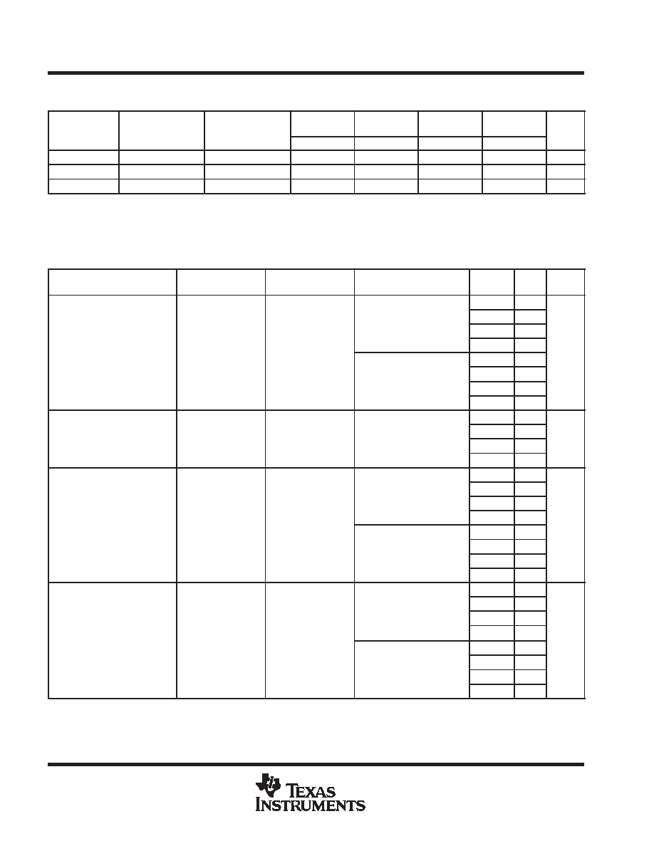
electrical characteristics over recommended operating free-air temperature range (unless
otherwise noted)
PARAMETER
TEST CONDITIONS
VCC
MIN
TYP
MAX
UNIT
V = V
or GND,
IS = 4 mA
1.65 V
12
30
ron
On-state switch resistance
VI = VCC or GND,
VC = VIH
IS = 8 mA
2.3 V
9
20
ron
On-state switch resistance
I
CC
VC = VIH
(see Figures 1 and 2)
IS = 24 mA
3 V
7.5
15
(see Figures 1 and 2)
IS = 32 mA
4.5 V
5.5
10
V = V
to GND,
IS = 4 mA
1.65 V
74.5
100
ron(p)
Peak on resistance
VI = VCC to GND,
VC = VIH
IS = 8 mA
2.3 V
20
30
ron(p)
Peak on resistance
I
CC
VC = VIH
(see Figures 1 and 2)
IS = 24 mA
3 V
11.5
20
(see Figures 1 and 2)
IS = 32 mA
4.5 V
7.5
15
IS(off)
Off-state switch leakage current
VI = VCC and VO = GND or
VI = GND and VO = VCC,
5.5 V
±
1
A
IS(off)
Off-state switch leakage current
I
CC
O
VI = GND and VO = VCC,
VC = VIL (see Figure 3)
5.5 V
±
0.1
µ
A
IS(on)
On-state switch leakage current
VI = VCC or GND, VC = VIH, VO = Open
5.5 V
±
1
A
IS(on)
On-state switch leakage current
VI = VCC or GND, VC = VIH, VO = Open
(see Figure 4)
5.5 V
±
0.1
µ
A
II
Control input current
VC = VCC or GND
5.5 V
±
1
A
II
Control input current
VC = VCC or GND
5.5 V
±
0.1
µ
A
ICC
Supply current
VC = VCC or GND
5.5 V
10
A
ICC
Supply current
VC = VCC or GND
5.5 V
1
µ
A
ICC
Supply current change
VC = VCC - 0.6 V
5.5 V
500
µ
A
Cic
Control input capacitance
5 V
2
pF
Cio(off)
Switch input/output capacitance
5 V
6
pF
Cio(on)
Switch input/output capacitance
5 V
13
pF
TA = 25
∞
C
SN74LVC1G66
SINGLE BILATERAL ANALOG SWITCH
SCES323H - JUNE 2001 - REVISED SEPTEMBER 2003
4
POST OFFICE BOX 655303
∑
DALLAS, TEXAS 75265
switching characteristics over recommended operating free-air temperature range (unless
otherwise noted) (see Figure 5)
PARAMETER
FROM
(INPUT)
TO
(OUTPUT)
VCC = 1.8 V
±
0.15 V
VCC = 2.5 V
±
0.2 V
VCC = 3.3 V
±
0.3 V
VCC = 5 V
±
0.5 V
UNIT
PARAMETER
(INPUT)
(OUTPUT)
MIN
MAX
MIN
MAX
MIN
MAX
MIN
MAX
UNIT
tpd
A or B
B or A
2
1.2
0.8
0.6
ns
ten
C
A or B
2.5
12
1.9
6.5
1.8
5
1.5
4.2
ns
tdisß
C
A or B
2.2
10
1.4
6.9
2
6.5
1.4
5
ns
tPLH and tPHL are the same as tpd. The propagation delay is the calculated RC time constant of the typical on-state resistance of the switch and
the specified load capacitance when driven by an ideal voltage source (zero output impedance).
tPZL and tPZH are the same as ten.
ß tPLZ and tPHZ are the same as tdis.
analog switch characteristics, T
A
= 25
∞
C
PARAMETER
FROM
(INPUT)
TO
(OUTPUT)
TEST CONDITIONS
VCC
TYP
UNIT
1.65 V
35
CL = 50 pF, RL = 600
,
fin = sine wave
2.3 V
120
L
L
fin = sine wave
(see Figure 6)
3 V
175
Frequency response∂
A or B
B or A
(see Figure 6)
4.5 V
195
MHz
Frequency response∂
(switch ON)
A or B
B or A
1.65 V
>
300
MHz
(switch ON)
CL = 5 pF, RL = 50
,
fin = sine wave
2.3 V
>
300
L
L
fin = sine wave
(see Figure 6)
3 V
>
300
(see Figure 6)
4.5 V
>
300
1.65 V
35
Crosstalk
C
A or B
CL = 50 pF, RL = 600
,
fin = 1 MHz (square wave)
2.3 V
50
mV
Crosstalk
(control input to signal output)
C
A or B
L
L
fin = 1 MHz (square wave)
(see Figure 7)
3 V
70
mV
(control input to signal output)
(see Figure 7)
4.5 V
100
1.65 V
-58
CL = 50 pF, RL = 600
,
fin = 1 MHz (sine wave)
2.3 V
-58
L
L
fin = 1 MHz (sine wave)
(see Figure 8)
3 V
-58
Feed-through attenuation#
A or B
B or A
(see Figure 8)
4.5 V
-58
dB
Feed-through attenuation#
(switch OFF)
A or B
B or A
1.65 V
-42
dB
(switch OFF)
CL = 5 pF, RL = 50
,
fin = 1 MHz (sine wave)
2.3 V
-42
L
L
fin = 1 MHz (sine wave)
(see Figure 8)
3 V
-42
(see Figure 8)
4.5 V
-42
C = 50 pF, R = 10 k ,
1.65 V
0.1
CL = 50 pF, RL = 10 k
,
fin = 1 kHz (sine wave)
2.3 V
0.025
L
L
fin = 1 kHz (sine wave)
(see Figure 9)
3 V
0.015
Sine-wave distortion
A or B
B or A
(see Figure 9)
4.5 V
0.01
%
Sine-wave distortion
A or B
B or A
C = 50 pF, R = 10 k ,
1.65 V
0.15
%
CL = 50 pF, RL = 10 k
,
fin = 10 kHz (sine wave)
2.3 V
0.025
L
L
fin = 10 kHz (sine wave)
(see Figure 9)
3 V
0.015
(see Figure 9)
4.5 V
0.01
∂ Adjust fin voltage to obtain 0 dBm at output. Increase fin frequency until dB meter reads -3 dB.
# Adjust fin voltage to obtain 0 dBm at input.
SN74LVC1G66
SINGLE BILATERAL ANALOG SWITCH
SCES323H - JUNE 2001 - REVISED SEPTEMBER 2003
5
POST OFFICE BOX 655303
∑
DALLAS, TEXAS 75265
operating characteristics, T
A
= 25
∞
C
PARAMETER
TEST CONDITIONS
VCC = 1.8 V VCC = 2.5 V VCC = 3.3 V
VCC = 5 V
UNIT
PARAMETER
TEST CONDITIONS
TYP
TYP
TYP
TYP
UNIT
Cpd
Power dissipation capacitance
f = 10 MHz
8
9
9
11
pF