www.ti.com
FEATURES
3
2
4
6
1
In1
In2
Y
GND
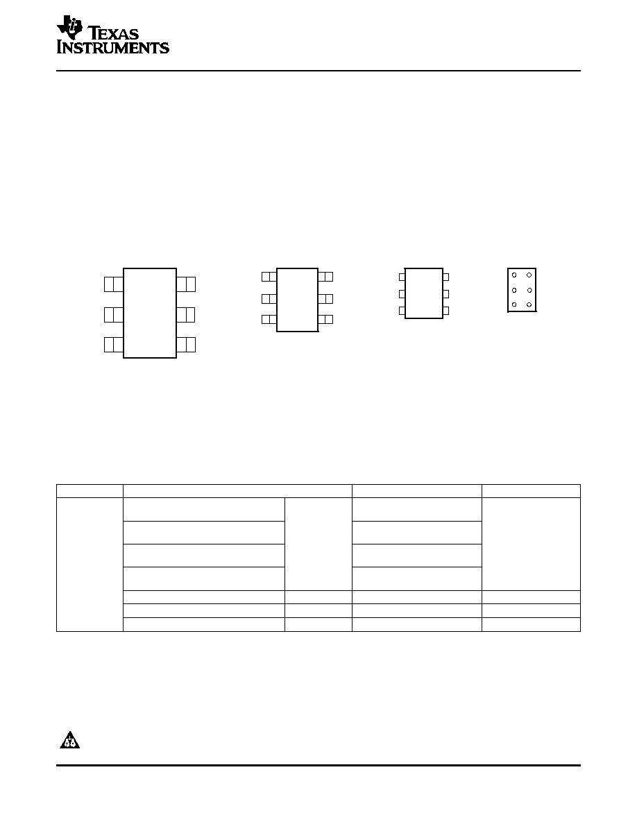
In0
DBV PACKAGE
(TOP VIEW)
YEA, YEP, YZA,
OR YZP PACKAGE
(BOTTOM VIEW)
DCK PACKAGE
(TOP VIEW)
3
2
4
6
1
In1
In2
Y
GND
In0
3
2
4
6
1
In1
In2
Y
GND
In0
In1
In0
In2
Y
GND
DRL PACKAGE
(TOP VIEW)
See mechanical drawings for dimensions.
1
4
2
3
6
V
CC
V
CC
V
CC
5
V
CC
5
5
5
DESCRIPTION/ORDERING INFORMATION
SN74LVC1G97
CONFIGURABLE MULTIPLE-FUNCTION GATE
SCES416I ≠ DECEMBER 2002 ≠ REVISED MARCH 2006
∑
Available in the Texas Instruments
∑
Latch-Up Performance Exceeds 100 mA Per
NanoStarTM and NanoFreeTM Packages
JESD 78, Class II
∑
Supports 5-V V
CC
Operation
∑
ESD Protection Exceeds JESD 22
∑
Inputs Accept Voltages to 5.5 V
≠ 2000-V Human-Body Model (A114-A)
∑
Max t
pd
of 6.3 ns at 3.3 V
≠ 200-V Machine Model (A115-A)
∑
Low Power Consumption, 10-
µ
A Max I
CC
≠ 1000-V Charged-Device Model (C101)
∑
±24-mA Output Drive at 3.3 V
∑
Choose From Nine Specific Logic Functions
∑
I
off
Supports Partial-Power-Down Mode
Operation
This configurable multiple-function gate is designed for 1.65-V to 5.5-V V
CC
operation.
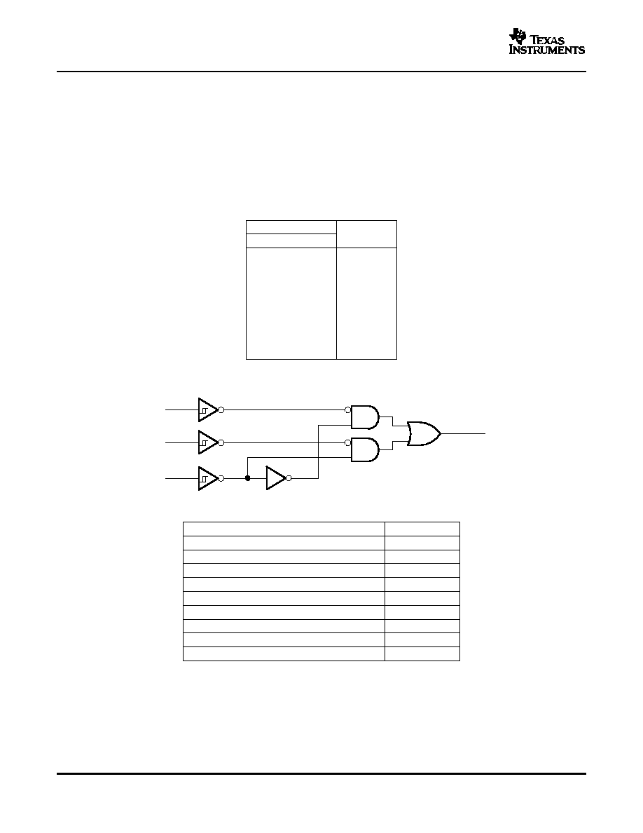
The SN74LVC1G97 features configurable multiple functions. The output state is determined by eight patterns of
3-bit input. The user can choose the logic functions MUX, AND, OR, NAND, NOR, inverter, and noninverter. All
inputs can be connected to V
CC
or GND.
ORDERING INFORMATION
T
A
PACKAGE
(1)
ORDERABLE PART NUMBER
TOP-SIDE MARKING
(2)
NanoStarTM ≠ WCSP (DSBGA)
SN74LVC1G97YEAR
0.17-mm Small Bump ≠ YEA
NanoFreeTM ≠ WCSP (DSBGA)
SN74LVC1G97YZAR
0.17-mm Small Bump ≠ YZA (Pb-free)
Tape and reel
_ _ _CS_
NanoStarTM ≠ WCSP (DSBGA)
SN74LVC1G97YEPR
0.23-mm Large Bump ≠ YEP
≠40∞C to 85∞C
NanoFreeTM ≠ WCSP (DSBGA)
SN74LVC1G97YZPR
0.23-mm Large Bump ≠ YZP (Pb-free)
SOT (SOT-23) ≠ DBV
Tape and reel
SN74LVC1G97DBVR
C97_
SOT (SC-70) ≠ DCK
Tape and reel
SN74LVC1G97DCKR
CS_
SOT (SOT-563) ≠ DRL
Reel of 4000
SN74LVC1G97DRLR
CS_
(1)
Package drawings, standard packing quantities, thermal data, symbolization, and PCB design guidelines are available at
www.ti.com/sc/package.
(2)
DBV/DCK/DRL: The actual top-side marking has one additional character that designates the assembly/test site.
YEA/YZA,YEP/YZP: The actual top-side marking has three preceding characters to denote year, month, and sequence code, and one
following character to designate the assembly/test site. Pin 1 identifier indicates solder-bump composition (1 = SnPb,
= Pb-free).
Please be aware that an important notice concerning availability, standard warranty, and use in critical applications of Texas
Instruments semiconductor products and disclaimers thereto appears at the end of this data sheet.
NanoStar, NanoFree are trademarks of Texas Instruments.
PRODUCTION DATA information is current as of publication date.
Copyright © 2002≠2006, Texas Instruments Incorporated
Products conform to specifications per the terms of the Texas
Instruments standard warranty. Production processing does not
necessarily include testing of all parameters.
www.ti.com
DESCRIPTION/ORDERING INFORMATION (CONTINUED)
3
1
6
In2
In1
In0
4
Y
SN74LVC1G97
CONFIGURABLE MULTIPLE-FUNCTION GATE
SCES416I ≠ DECEMBER 2002 ≠ REVISED MARCH 2006
This device functions as an independent gate, but because of Schmitt action, it may have different input
threshold levels for positive-going (V
T+
) and negative-going (V
T≠
) signals.
NanoStarTM and NanoFreeTM package technology is a major breakthrough in IC packaging concepts, using the
die as the package.
This device is fully specified for partial-power-down applications using I
off
. The I
off
circuitry disables the outputs,
preventing damaging current backflow through the device when it is powered down.
FUNCTION TABLE
INPUTS
OUTPUT
In2
In1
In0
Y
L
L
L
L
L
L
H
L
L
H
L
H
L
H
H
H
H
L
L
L
H
L
H
H
H
H
L
L
H
H
H
H
LOGIC DIAGRAM (POSITIVE LOGIC)
FUNCTION SELECTION TABLE
LOGIC FUNCTION
FIGURE NO.
2-to-1 data selector
1
2-input AND gate
2
2-input OR gate with one inverted input
3
2-input NAND gate with one inverted input
3
2-input AND gate with one inverted input
4
2-input NOR gate with one inverted input
4
2-input OR gate
5
Inverter
6
Noninverted buffer
7
2
Submit Documentation Feedback
www.ti.com
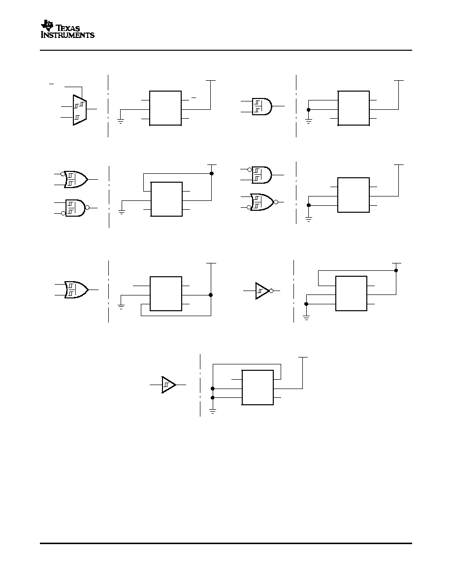
LOGIC CONFIGURATIONS
1
2
3
6
5
4
A
Y
A/B
V
CC
A
B
A/B
Y
B
GND
1
2
3
6
5
4
B
Y
A
V
CC
A
Y
B
GND
1
2
3
6
5
4
B
Y
A
V
CC
A
Y
B
A
Y
B
GND
A
Y
B
A
Y
B
1
2
3
6
5
4
B
Y
A
V
CC
GND
1
2
3
6
5
4
B
Y
A
V
CC
A
Y
B
GND
1
2
3
6
5
4
Y
A
V
CC
Y
A
GND
1
2
3
6
5
4
Y
V
CC
Y
A
GND
A
SN74LVC1G97
CONFIGURABLE MULTIPLE-FUNCTION GATE
SCES416I ≠ DECEMBER 2002 ≠ REVISED MARCH 2006
Figure 1. 2-to-1 Data Selector
Figure 2. 2-Input AND Gate
Figure 3. 2-Input OR Gate With One Inverted Input
Figure 4. 2-Input AND Gate With One Inverted Input
2-Input NAND Gate With One Inverted Input
2-Input NOR Gate With One Inverted Input
Figure 5. 2-Input OR Gate
Figure 6. Inverter
Figure 7. Noninverted Buffer
3
Submit Documentation Feedback
www.ti.com
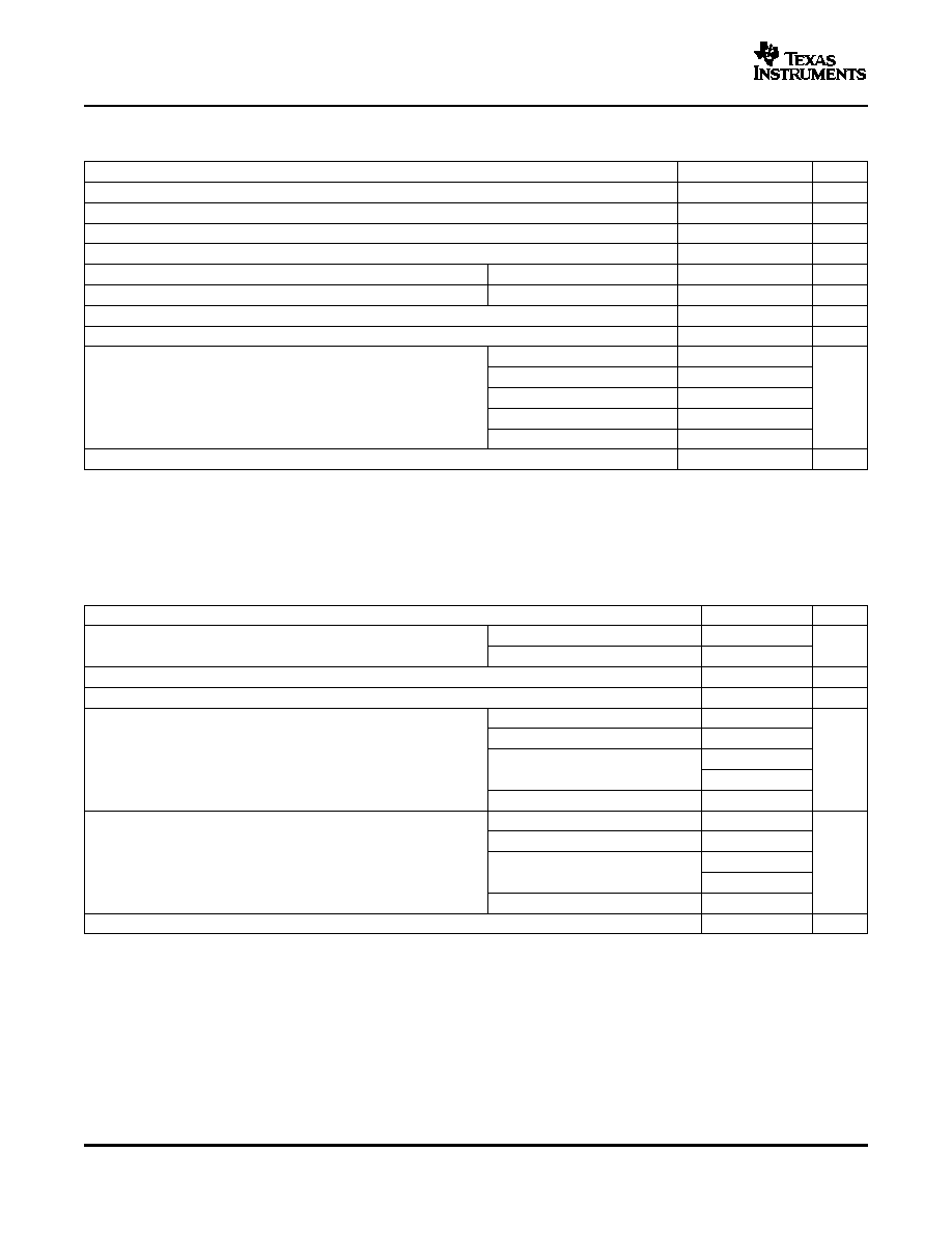
Absolute Maximum Ratings
(1)
Recommended Operating Conditions
(1)
SN74LVC1G97
CONFIGURABLE MULTIPLE-FUNCTION GATE
SCES416I ≠ DECEMBER 2002 ≠ REVISED MARCH 2006
over operating free-air temperature range (unless otherwise noted)
MIN
MAX
UNIT
V
CC
Supply voltage range
≠0.5
6.5
V
V
I
Input voltage range
(2)
≠0.5
6.5
V
V
O
Voltage range applied to any output in the high-impedance or power-off state
(2)
≠0.5
6.5
V
V
O
Voltage range applied to any output in the high or low state
(2) (3)
≠0.5
V
CC
+ 0.5
V
I
IK
Input clamp current
V
I
< 0
≠50
mA
I
OK
Output clamp current
V
O
< 0
≠50
mA
I
O
Continuous output current
±50
mA
Continuous current through V
CC
or GND
±100
mA
DBV package
165
DCK package
259
JA
Package thermal impedance
(4)
DRL package
142
∞C/W
YEA/YZA package
143
YEP/YZP package
123
T
stg
Storage temperature range
≠65
150
∞C
(1)
Stresses beyond those listed under "absolute maximum ratings" may cause permanent damage to the device. These are stress ratings
only, and functional operation of the device at these or any other conditions beyond those indicated under "recommended operating
conditions" is not implied. Exposure to absolute-maximum-rated conditions for extended periods may affect device reliability.
(2)
The input and output negative-voltage ratings may be exceeded if the input and output current ratings are observed.
(3)
The value of V
CC
is provided in the recommended operating conditions table.
(4)
The package thermal impedance is calculated in accordance with JESD 51-7.
MIN
MAX
UNIT
Operating
1.65
5.5
V
CC
Supply voltage
V
Data retention only
1.5
V
I
Input voltage
0
5.5
V
V
O
Output voltage
0
V
CC
V
V
CC
= 1.65 V
≠4
V
CC
= 2.3 V
≠8
I
OH
High-level output current
≠16
mA
V
CC
= 3 V
≠24
V
CC
= 4.5 V
≠32
V
CC
= 1.65 V
4
V
CC
= 2.3 V
8
I
OL
Low-level output current
16
mA
V
CC
= 3 V
24
V
CC
= 4.5 V
32
T
A
Operating free-air temperature
≠40
85
∞C
(1)
All unused inputs of the device must be held at V
CC
or GND to ensure proper device operation. Refer to the TI application report,
Implications of Slow or Floating CMOS Inputs, literature number SCBA004.
4
Submit Documentation Feedback
www.ti.com
Electrical Characteristics
SN74LVC1G97
CONFIGURABLE MULTIPLE-FUNCTION GATE
SCES416I ≠ DECEMBER 2002 ≠ REVISED MARCH 2006
over recommended operating free-air temperature range (unless otherwise noted)
PARAMETER
TEST CONDITIONS
V
CC
MIN
TYP
(1)
MAX
UNIT
1.65 V
0.79
1.16
2.3 V
1.11
1.56
V
T+
Positive-going input
3 V
1.5
1.87
V
threshold voltage
4.5 V
2.16
2.74
5.5 V
2.61
3.33
1.65 V
0.35
0.62
2.3 V
0.58
0.87
V
T≠
Negative-going input
3 V
0.84
1.19
V
threshold voltage
4.5 V
1.41
1.9
5.5 V
1.87
2.29
1.65 V
0.3
0.62
2.3 V
0.4
0.8
V
T
3 V
0.53
0.87
V
Hysteresis (V
T+
≠ V
T≠
)
4.5 V
0.71
1.04
5.5 V
0.71
1.11
I
OH
= ≠100
µ
A
1.65 V to 5.5 V
V
CC
≠ 0.1
I
OH
= ≠4 mA
1.65 V
1.2
I
OH
= ≠8 mA
2.3 V
1.9
V
OH
V
I
OH
= ≠16 mA
2.4
3 V
I
OH
= ≠24 mA
2.3
I
OH
= ≠32 mA
4.5 V
3.8
I
OL
= 100
µ
A
1.65 V to 5.5 V
0.1
I
OL
= 4 mA
1.65 V
0.45
I
OL
= 8 mA
2.3 V
0.3
V
OL
V
I
OL
= 16 mA
0.4
3 V
I
OL
= 24 mA
0.55
I
OL
= 32 mA
4.5 V
0.55
I
I
V
I
= 5.5 V or GND
0 to 5.5 V
±5
µ
A
I
off
V
I
or V
O
= 5.5 V
0
±10
µ
A
I
CC
V
I
= 5.5 V or GND, I
O
= 0
1.65 V to 5.5 V
10
µ
A
One input at V
CC
≠ 0.6 V,
I
CC
3 V to 5.5 V
500
µ
A
Other inputs at V
CC
or GND
C
i
V
I
= V
CC
or GND
3.3 V
3.5
pF
(1)
All typical values are at V
CC
= 3.3 V, T
A
= 25∞C.
5
Submit Documentation Feedback