SN74LVC1T45
SINGLE BIT DUAL SUPPLY BUS TRANSCEIVER
WITH CONFIGURABLE VOLTAGE TRANSLATION AND 3 STATE OUTPUTS
SCES515E - DECEMBER 2003 - REVISED MAY 2004
1
POST OFFICE BOX 655303
∑
DALLAS, TEXAS 75265
D
Available in the Texas Instruments
NanoStar
and NanoFree
Packages
D
Fully Configurable Dual-Rail Design Allows
Each Port to Operate Over the Full 1.65-V to
5.5-V Power-Supply Range
D
V
CC
Isolation Feature - If Either V
CC
Input
Is at GND, Both Ports Are in the
High-Impedance State
D
DIR Input Circuit Referenced to V
CCA
D
Low Power Consumption, 4-
µ
A Max I
CC
D
±
24-mA Output Drive at 3.3 V
D
I
off
Supports Partial-Power-Down Mode
Operation
D
Max Data Rates
- 420 Mbps (3.3-V to 5-V Translation)
- 210 Mbps (Translate to 3.3 V)
- 140 Mbps (Translate to 2.5 V)
- 75 Mbps (Translate to 1.8 V)
D
Latch-Up Performance Exceeds 100 mA Per
JESD 78, Class II
D
ESD Protection Exceeds JESD 22
- 2000-V Human-Body Model (A114-A)
- 200-V Machine Model (A115-A)
- 1000-V Charged-Device Model (C101)
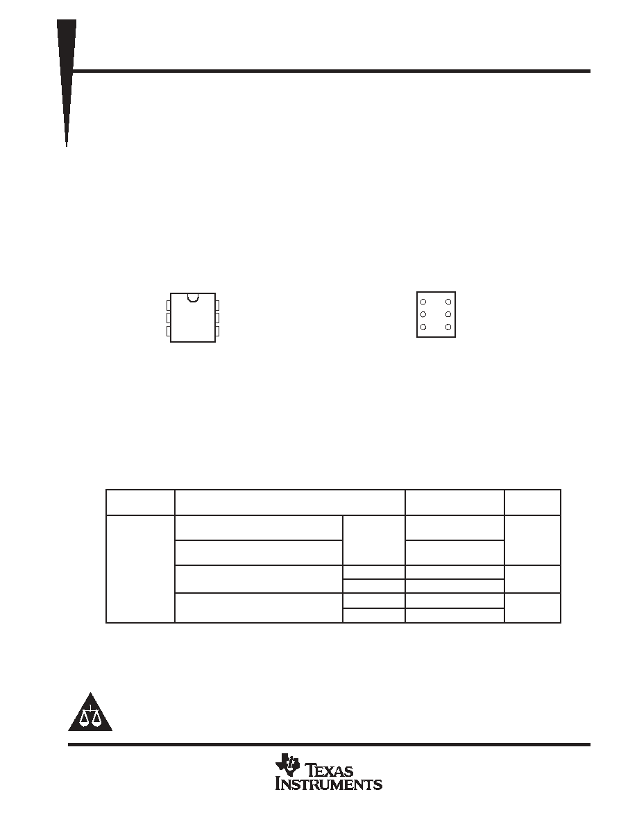
DBV OR DCK PACKAGE
(TOP VIEW)
1
2
3
6
5
4
V
CCA
GND
A
V
CCB
DIR
B
3
2
1
4
5
6
A
GND
V
CCA
B
DIR
V
CCB
YEP OR YZP PACKAGE
(BOTTOM VIEW)
description/ordering information
This single-bit noninverting bus transceiver uses two separate configurable power-supply rails. The A port is
designed to track V
CCA
. V
CCA
accepts any supply voltage from 1.65 V to 5.5 V. The B port is designed to track
V
CCB
. V
CCB
accepts any supply voltage from 1.65 V to 5.5 V. This allows for universal low-voltage bidirectional
translation between any of the 1.8-V, 2.5-V, 3.3-V, and 5-V voltage nodes.
The SN74LVC1T45 is designed for asynchronous communication between data buses. The device transmits
data from the A bus to the B bus or from the B bus to the A bus, depending on the logic level at the
direction-control (DIR) input.
ORDERING INFORMATION
TA
PACKAGE
ORDERABLE
PART NUMBER
TOP-SIDE
MARKING
NanoStar
- WCSP (DSBGA)
0.23-mm Large Bump - YEP
Reel of 3000
SN74LVC1T45YEPR
_ _ _TA_
-40 C to 85 C
NanoFree
- WCSP (DSBGA)
0.23-mm Large Bump - YZP (Pb-free)
Reel of 3000
SN74LVC1T45YZPR
_ _ _TA_
-40
∞
C to 85
∞
C
SOT (SOT-23) - DBV
Reel of 3000
SN74LVC1T45DBVR
CT1_
SOT (SOT-23) - DBV
Reel of 250
SN74LVC1T45DBVT
CT1_
SOT (SC-70) - DCK
Reel of 3000
SN74LVC1T45DCKR
TA_
SOT (SC-70) - DCK
Reel of 250
SN74LVC1T45DCKT
TA_
Package drawings, standard packing quantities, thermal data, symbolization, and PCB design guidelines are available at
www.ti.com/sc/package.
DBV/DCK: The actual top-side marking has one additional character that designates the assembly/test site.
YEP/YZP: The actual top-side marking has three preceding characters to denote year, month, and sequence code, and one
following character to designate the assembly/test site. Pin 1 identifier indicates solder-bump composition
(1 = SnPb,
∑
= Pb-free).
Copyright
2004, Texas Instruments Incorporated
NanoStar and NanoFree are trademarks of Texas Instruments.
Please be aware that an important notice concerning availability, standard warranty, and use in critical applications of
Texas Instruments semiconductor products and disclaimers thereto appears at the end of this data sheet.
PRODUCTION DATA information is current as of publication date.
Products conform to specifications per the terms of Texas Instruments
standard warranty. Production processing does not necessarily include
testing of all parameters.

SN74LVC1T45
SINGLE BIT DUAL SUPPLY BUS TRANSCEIVER
WITH CONFIGURABLE VOLTAGE TRANSLATION AND 3 STATE OUTPUTS
SCES515E - DECEMBER 2003 - REVISED MAY 2004
2
POST OFFICE BOX 655303
∑
DALLAS, TEXAS 75265
description/ordering information (continued)
The SN74LVC1T45 is designed so that the DIR input circuit is supplied by V
CCA
.
This device is fully specified for partial-power-down applications using I
off
. The I
off
circuitry disables the outputs,
preventing damaging current backflow through the device when it is powered down.
The V
CC
isolation feature ensures that if either V
CC
input is at GND, both ports are in the high-impedance state.
NanoStar
and NanoFree
package technology is a major breakthrough in IC packaging concepts, using the
die as the package.
FUNCTION TABLE
INPUT
OPERATION
DIR
OPERATION
L
B data to A bus
H
A data to B bus
logic diagram (positive logic)
B
DIR
5
4
A
3
VCCA
VCCB

SN74LVC1T45
SINGLE BIT DUAL SUPPLY BUS TRANSCEIVER
WITH CONFIGURABLE VOLTAGE TRANSLATION AND 3 STATE OUTPUTS
SCES515E - DECEMBER 2003 - REVISED MAY 2004
3
POST OFFICE BOX 655303
∑
DALLAS, TEXAS 75265
absolute maximum ratings over operating free-air temperature range (unless otherwise noted)
Supply voltage range, V
CCA
and V
CCB
-0.5 V to 6.5 V
. . . . . . . . . . . . . . . . . . . . . . . . . . . . . . . . . . . . . . . . . . . . . .
Input voltage range, V
I
(see Note 1)
-0.5 V to 6.5 V
. . . . . . . . . . . . . . . . . . . . . . . . . . . . . . . . . . . . . . . . . . . . . . . . .
Voltage range applied to any output in the high-impedance or power-off state, V
O
(see Note 1)
-0.5 V to 6.5 V
. . . . . . . . . . . . . . . . . . . . . . . . . . . . . . . . . . . . . . . . . . . . . . . . . . . . . . . . . . . . . . . . . . .
Voltage range applied to any output in the high or low state, V
O
(see Notes 1 and 2): A port
-0.5 V to V
CCA
+ 0.5V
. . . . . . . . . . . . . . . . . . . . . . . . . . . . . . . . . . . . . . . . . . . . . . .
B port
-0.5 V to V
CCB
+ 0.5V
. . . . . . . . . . . . . . . . . . . . . . . . . . . . . . . . . . . . . . . . . . . . . . .
Input clamp current, I
IK
(V
I
< 0)
-50 mA
. . . . . . . . . . . . . . . . . . . . . . . . . . . . . . . . . . . . . . . . . . . . . . . . . . . . . . . . . . .
Output clamp current, I
OK
(V
O
< 0)
-50 mA
. . . . . . . . . . . . . . . . . . . . . . . . . . . . . . . . . . . . . . . . . . . . . . . . . . . . . . . .
Continuous output current, I
O
±
50 mA
. . . . . . . . . . . . . . . . . . . . . . . . . . . . . . . . . . . . . . . . . . . . . . . . . . . . . . . . . . . . .
Continuous current through V
CC
or GND
±
100 mA
. . . . . . . . . . . . . . . . . . . . . . . . . . . . . . . . . . . . . . . . . . . . . . . . . .
Package thermal impedance,
JA
(see Note 3): DBV package
165
∞
C/W
. . . . . . . . . . . . . . . . . . . . . . . . . . . . . . .
DCK package
259
∞
C/W
. . . . . . . . . . . . . . . . . . . . . . . . . . . . . . .
YEP/YZP package
123
∞
C/W
. . . . . . . . . . . . . . . . . . . . . . . . . . .
Storage temperature range, T
stg
-65
∞
C to 150
∞
C
. . . . . . . . . . . . . . . . . . . . . . . . . . . . . . . . . . . . . . . . . . . . . . . . . . .
Stresses beyond those listed under "absolute maximum ratings" may cause permanent damage to the device. These are stress ratings only, and
functional operation of the device at these or any other conditions beyond those indicated under "recommended operating conditions" is not
implied. Exposure to absolute-maximum-rated conditions for extended periods may affect device reliability.
NOTES:
1. The input and output negative-voltage ratings may be exceeded if the input and output clamp-current ratings are observed.
2. The value of VCC is provided in the recommended operating conditions table.
3. The package thermal impedance is calculated in accordance with JESD 51-7.

SN74LVC1T45
SINGLE BIT DUAL SUPPLY BUS TRANSCEIVER
WITH CONFIGURABLE VOLTAGE TRANSLATION AND 3 STATE OUTPUTS
SCES515E - DECEMBER 2003 - REVISED MAY 2004
4
POST OFFICE BOX 655303
∑
DALLAS, TEXAS 75265
recommended operating conditions (see Notes 4 through 8)
VCCI
VCCO
MIN
MAX
UNIT
VCCA
Supply voltage
1.65
5.5
V
VCCB
Supply voltage
1.65
5.5
V
1.65 V to 1.95 V
VCCI
◊
0.65
VIH
High-level input
Data inputs
2.3 V to 2.7 V
1.7
V
VIH
High-level input
voltage
Data inputs
(see Note 7)
3 V to 3.6 V
2
V
voltage
(see Note 7)
4.5 V to 5.5 V
VCCI
◊
0.7
1.65 V to 1.95 V
VCCI
◊
0.35
VIL
Low-level input
Data inputs
2.3 V to 2.7 V
0.7
V
VIL
Low-level input
voltage
Data inputs
(see Note 7)
3 V to 3.6 V
0.8
V
voltage
(see Note 7)
4.5 V to 5.5 V
VCCI
◊
0.3
DIR
1.65 V to 1.95 V
VCCA
◊
0.65
VIH
High-level input
DIR
(Referenced to VCCA)
2.3 V to 2.7 V
1.7
V
VIH
High-level input
voltage
(Referenced to VCCA)
(see Note 8)
3 V to 3.6 V
2
V
voltage
(see Note 8)
4.5 V to 5.5 V
VCCA
◊
0.7
DIR
1.65 V to 1.95 V
VCCA
◊
0.35
VIL
Low-level input
DIR
(Referenced to VCCA)
2.3 V to 2.7 V
0.7
V
VIL
Low-level input
voltage
(Referenced to VCCA)
(see Note 8)
3 V to 3.6 V
0.8
V
voltage
(see Note 8)
4.5 V to 5.5 V
VCCA
◊
0.3
VI
Input voltage
0
5.5
V
VO
Output voltage
0
VCCO
V
1.65 V to 1.95 V
-4
IOH
High-level output current
2.3 V to 2.7 V
-8
mA
IOH
High-level output current
3 V to 3.6 V
-24
mA
4.5 V to 5.5 V
-32
1.65 V to 1.95 V
4
IOL
Low-level output current
2.3 V to 2.7 V
8
mA
IOL
Low-level output current
3 V to 3.6 V
24
mA
4.5 V to 5.5 V
32
1.65 V to 1.95 V
20
Input transition rise or
Data input
2.3 V to 2.7 V
20
t/
v
Input transition rise or
fall rate
Data input
3 V to 3.6 V
10
ns/V
t/ v
fall rate
4.5 V to 5.5 V
5
ns/V
Control input
1.65 V to 5.5 V
5
TA
Operating free-air temperature
-40
85
∞
C
NOTES:
4. VCCI is the VCC associated with the data input port.
5. VCCO is the VCC associated with the output port.
6. All unused data inputs of the device must be held at VCCI or GND to ensure proper device operation. Refer to the TI application report,
Implications of Slow or Floating CMOS Inputs, literature number SCBA004.
7. For VCCI values not specified in the data sheet, VIH(min) = VCCI x 0.7 V, VIL(max) = VCCI x 0.3 V.
8. For VCCI values not specified in the data sheet, VIH(min) = VCCA x 0.7 V, VIL(max) = VCCA x 0.3 V.

SN74LVC1T45
SINGLE BIT DUAL SUPPLY BUS TRANSCEIVER
WITH CONFIGURABLE VOLTAGE TRANSLATION AND 3 STATE OUTPUTS
SCES515E - DECEMBER 2003 - REVISED MAY 2004
5
POST OFFICE BOX 655303
∑
DALLAS, TEXAS 75265
electrical characteristics over recommended operating free-air temperature range (unless
otherwise noted) (see Notes 9 and 10)
PARAMETER
TEST CONDITIONS
VCCA
VCCB
TA = 25
∞
C
-40
∞
C to 85
∞
C
UNIT
PARAMETER
TEST CONDITIONS
VCCA
VCCB
MIN
TYP
MAX
MIN
MAX
UNIT
IOH = -100
µ
A,
VI = VIH
1.65 V to 4.5 V
1.65 V to 4.5 V
VCCO-0.1
IOH = -4 mA,
VI = VIH
1.65V
1.65 V
1.2
VOH
IOH = -8 mA,
VI = VIH
2.3 V
2.3 V
1.9
V
VOH
IOH = -24 mA,
VI = VIH
3 V
3 V
2.4
V
IOH = -32 mA,
VI = VIH
4.5 V
4.5 V
3.8
IOL = 100
µ
A,
VI = VIL
1.65 V to 4.5 V
1.65 V to 4.5 V
0.1
IOL = 4 mA,
VI = VIL
1.65 V
1.65 V
0.45
VOL
IOL = 8 mA,
VI = VIL
2.3 V
2.3 V
0.3
V
VOL
IOL = 24 mA,
VI = VIL
3 V
3 V
0.55
V
IOL = 32 mA,
VI = VIL
4.5 V
4.5 V
0.55
II
DIR
input
VI = VCCA or GND
1.65 V to 5.5 V
1.65 V to 5.5 V
±
1
±
2
µ
A
Ioff
A port
VI or VO = 0 to 5.5 V
0 V
0 to 5.5 V
±
1
±
2
A
Ioff
B port
VI or VO = 0 to 5.5 V
0 to 5.5 V
0 V
±
1
±
2
µ
A
IOZ
A or B
ports
VO = VCCO or GND
1.65 V to 5.5 V
1.65 V to 5.5 V
±
1
±
2
µ
A
VI = VCCI or
1.65 V to 5.5 V
1.65 V to 5.5 V
3
ICCA
VI = VCCI or
GND
IO = 0
5.5 V
0 V
2
µ
A
ICCA
GND
IO = 0
0 V
5.5 V
0
µ
A
VI = VCCI or
1.65 V to 5.5 V
1.65 V to 5.5 V
3
ICCB
VI = VCCI or
GND
IO = 0
5.5 V
0 V
0
µ
A
ICCB
GND
IO = 0
0 V
5.5 V
2
µ
A
ICCA + ICCB
VI = VCCI or
GND
IO = 0
1.65 V to 5.5 V
1.65 V to 5.5 V
4
µ
A
A port
A port at VCCA - 0.6 V,
DIR at VCCA, B port = OPEN
50
ICCA
DIR
DIR at VCCA - 0.6 V,
B port = OPEN,
A port at VCCA or GND
3 V to 5.5 V
3 V to 5.5 V
50
µ
A
ICCB B port
B port at VCCB - 0.6 V,
DIR at GND, A port = OPEN
3 V to 5.5 V
3 V to 5.5 V
50
µ
A
Ci
DIR
input
VI = VCCA or GND
3.3 V
3.3 V
2.5
pF
Cio
A or B
ports
VO = VCCA/B or GND
3.3 V
3.3 V
6
pF
NOTES:
9. VCCO is the VCC associated with the output port.
10. VCCI is the VCC associated with the input port.