www.ti.com
FEATURES
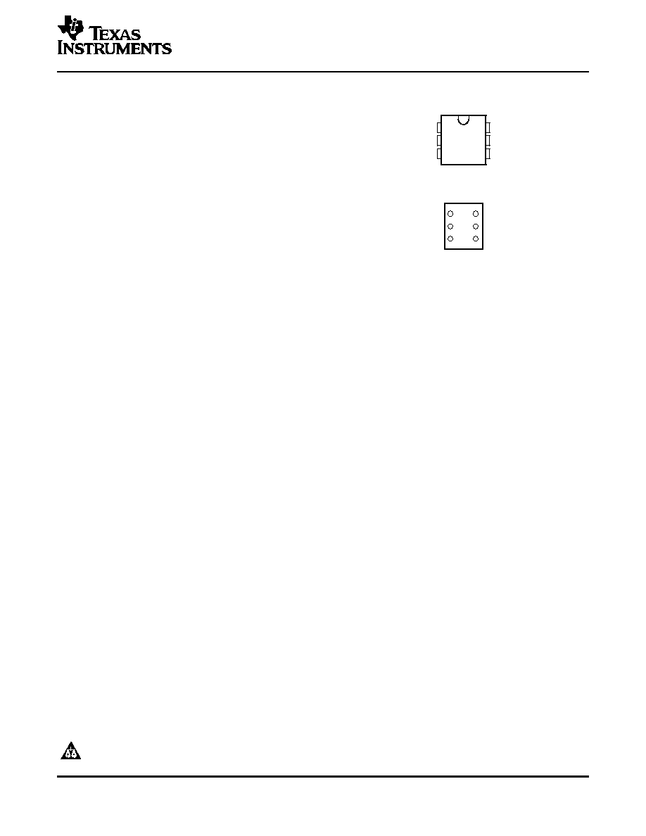
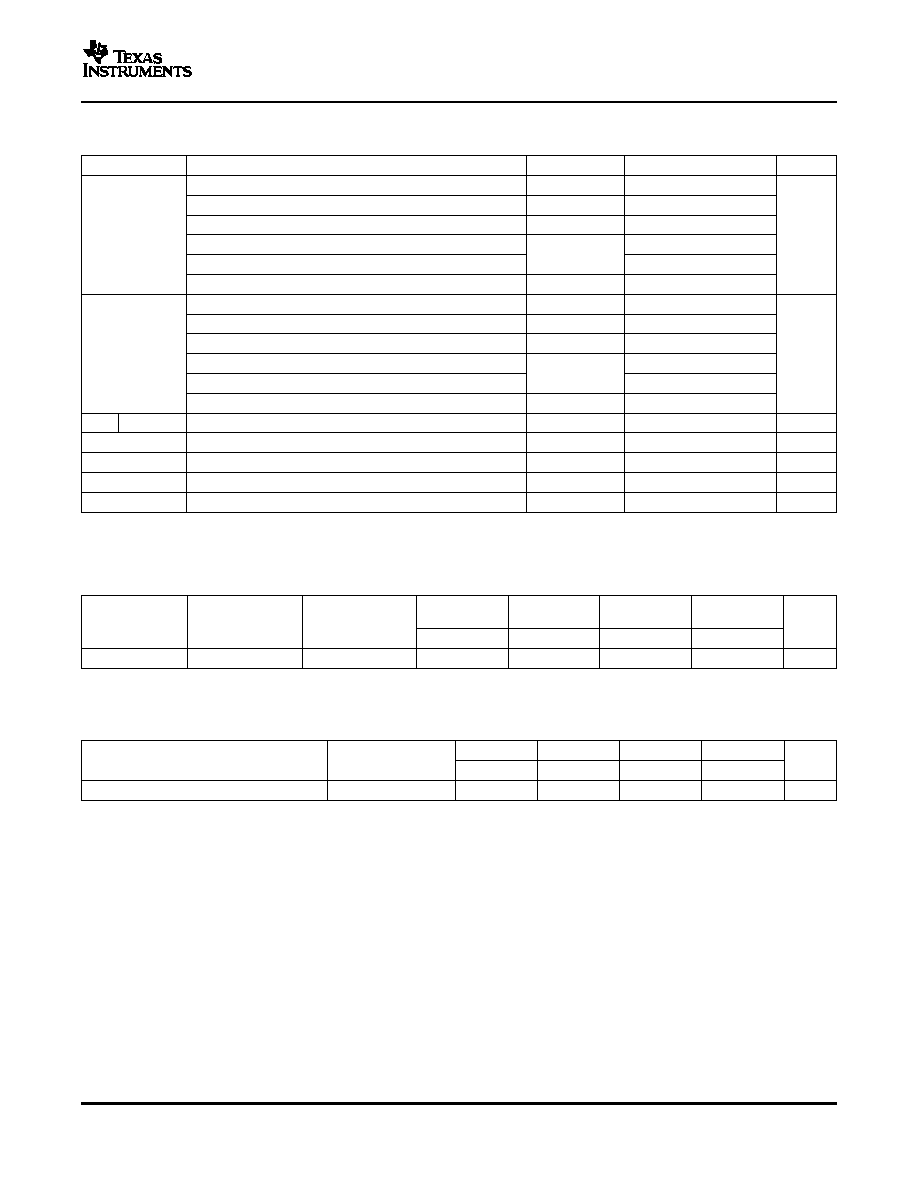
DBV, DCK, OR DRL PACKAGE
(TOP VIEW)
1
2
3
6
5
4
1A
GND
2A
1Y
V
CC
2Y
3
2
1
4
5
6
2A
GND
1A
2Y
V
CC
1Y
YEA, YEP, YZA, OR YZP PACKAGE
(BOTTOM VIEW)
DESCRIPTION/ORDERING INFORMATION
SN74LVC2G34
DUAL BUFFER GATE
SCES359F ≠ AUGUST 2001 ≠ REVISED APRIL 2005
∑
Available in the Texas Instruments
NanoStarTM and NanoFreeTM Packages
∑
Supports 5-V V
CC
Operation
∑
Inputs Accept Voltages to 5.5 V
∑
Max t
pd
of 4.1 ns at 3.3 V
∑
Low Power Consumption, 10-
µ
A Max I
CC
∑
24-mA Output Drive at 3.3 V
∑
Typical V
OLP
(Output Ground Bounce) < 0.8 V
at V
CC
= 3.3 V, T
A
= 25 C
∑
Typical V
OHV
(Output V
OH
Undershoot) > 2 V
at V
CC
= 3.3 V, T
A
= 25 C
∑
I
off
Supports Partial-Power-Down Mode
Operation
∑
Latch-Up Performance Exceeds 100 mA Per
JESD 78, Class II
∑
ESD Protection Exceeds JESD 22
≠ 2000-V Human-Body Model (A114-A)
≠ 200-V Machine Model (A115-A)
≠ 1000-V Charged-Device Model (C101)
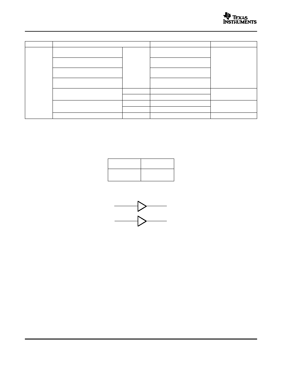
This dual buffer gate is designed for 1.65-V to 5.5-V V
CC
operation. The SN74LVC2G34 performs the Boolean
function Y = A in positive logic.
NanoStarTM and NanoFreeTM package technology is a major breakthrough in IC packaging concepts, using the
die as the package.
This device is fully specified for partial-power-down applications using I
off
. The I
off
circuitry disables the outputs,
preventing damaging current backflow through the device when it is powered down.
Please be aware that an important notice concerning availability, standard warranty, and use in critical applications of Texas
Instruments semiconductor products and disclaimers thereto appears at the end of this data sheet.
NanoStar, NanoFree are trademarks of Texas Instruments.
PRODUCTION DATA information is current as of publication date.
Copyright © 2001≠2005, Texas Instruments Incorporated
Products conform to specifications per the terms of the Texas
Instruments standard warranty. Production processing does not
necessarily include testing of all parameters.
www.ti.com
LOGIC DIAGRAM (POSITIVE LOGIC)
1A
1Y
1
6
2A
2Y
3
4
SN74LVC2G34
DUAL BUFFER GATE
SCES359F ≠ AUGUST 2001 ≠ REVISED APRIL 2005
ORDERING INFORMATION
T
A
PACKAGE
(1)
ORDERABLE PART NUMBER
TOP-SIDE MARKING
(2)
NanoStarTM ≠ WCSP (DSBGA)
SN74LVC2G34YEAR
0.17-mm Small Bump ≠ YEA
NanoFreeTM ≠ WCSP (DSBGA)
SN74LVC2G34YZAR
0.17-mm Small Bump ≠ YZA (Pb-free)
Reel of 3000
_ _ _C9_
NanoStarTM ≠ WCSP (DSBGA)
SN74LVC2G34YEPR
0.23-mm Large Bump ≠ YEP
NanoFreeTM ≠ WCSP (DSBGA)
≠40
∞
C to 85
∞
C
SN74LVC2G34YZPR
0.23-mm Large Bump ≠ YZP (Pb-free)
Reel of 3000
SN74LVC2G34DBVR
SOT (SOT-23) ≠ DBV
C34_
Reel of 250
SN74LVC2G34DBVT
Reel of 3000
SN74LVC2G34DCKR
SOT (SC-70) ≠ DCK
C9_
Reel of 250
SN74LVC2G34DCKT
SOT (SOT-533) ≠ DRL
Reel of 4000
SN74LVC2G34DRLR
PREVIEW
(1)
Package drawings, standard packing quantities, thermal data, symbolization, and PCB design guidelines are available at
www.ti.com/sc/package.
(2)
DBV/DCK: The actual top-side marking has one additional character that designates the assembly/test site.
YEA/YZA, YEP/YZP: The actual top-side marking has three preceding characters to denote year, month, and sequence code, and one
following character to designate the assembly/test site. Pin 1 identifier indicates solder-bump composition (1 = SnPb,
= Pb-free).
FUNCTION TABLE
(EACH GATE)
INPUT
OUTPUT
A
Y
H
H
L
L
2
www.ti.com
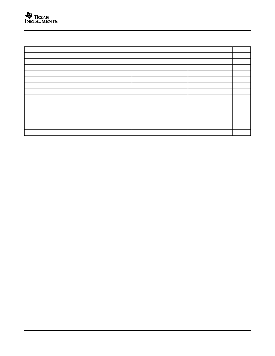
Absolute Maximum Ratings
(1)
SN74LVC2G34
DUAL BUFFER GATE
SCES359F ≠ AUGUST 2001 ≠ REVISED APRIL 2005
over operating free-air temperature range (unless otherwise noted)
MIN
MAX
UNIT
V
CC
Supply voltage range
≠0.5
6.5
V
V
I
Input voltage range
(2)
≠0.5
6.5
V
V
O
Voltage range applied to any output in the high-impedance or power-off state
(2)
≠0.5
6.5
V
V
O
Voltage range applied to any output in the high or low state
(2) (3)
≠0.5
V
CC
+ 0.5
V
I
IK
Input clamp current
V
I
< 0
≠50
mA
I
OK
Output clamp current
V
O
< 0
≠50
mA
I
O
Continuous output current
50
mA
Continuous current through V
CC
or GND
100
mA
DBV package
165
DCK package
259
JA
Package thermal impedance
(4)
DRL package
142
C/W
YEA/YZA package
143
YEP/YZP package
123
T
stg
Storage temperature range
≠65
150
C
(1)
Stresses beyond those listed under "absolute maximum ratings" may cause permanent damage to the device. These are stress ratings
only, and functional operation of the device at these or any other conditions beyond those indicated under "recommended operating
conditions" is not implied. Exposure to absolute-maximum-rated conditions for extended periods may affect device reliability.
(2)
The input negative-voltage and output voltage ratings may be exceeded if the input and output current ratings are observed.
(3)
The value of V
CC
is provided in the recommended operating conditions table.
(4)
The package thermal impedance is calculated in accordance with JESD 51-7.
3
www.ti.com
Recommended Operating Conditions
(1)
SN74LVC2G34
DUAL BUFFER GATE
SCES359F ≠ AUGUST 2001 ≠ REVISED APRIL 2005
MIN
MAX
UNIT
Operating
1.65
5.5
V
CC
Supply voltage
V
Data retention only
1.5
V
CC
= 1.65 V to 1.95 V
0.65
V
CC
V
CC
= 2.3 V to 2.7 V
1.7
V
IH
High-level input voltage
V
V
CC
= 3 V to 3.6 V
2
V
CC
= 4.5 V to 5.5 V
0.7
V
CC
V
CC
= 1.65 V to 1.95 V
0.35
V
CC
V
CC
= 2.3 V to 2.7 V
0.7
V
IL
Low-level input voltage
V
V
CC
= 3 V to 3.6 V
0.8
V
CC
= 4.5 V to 5.5 V
0.3
V
CC
V
I
Input voltage
0
5.5
V
V
O
Output voltage
0
V
CC
V
V
CC
= 1.65 V
≠4
V
CC
= 2.3 V
≠8
I
OH
High-level output current
≠16
mA
V
CC
= 3 V
≠24
V
CC
= 4.5 V
≠32
V
CC
= 1.65 V
4
V
CC
= 2.3 V
8
I
OL
Low-level output current
16
mA
V
CC
= 3 V
24
V
CC
= 4.5 V
32
V
CC
= 1.8 V
0.15 V, 2.5 V
0.2 V
20
?t/?v
Input transition rise or fall rate
V
CC
= 3.3 V
0.3 V
10
ns/V
V
CC
= 5 V
0.5 V
5
T
A
Operating free-air temperature
≠40
85
C
(1)
All unused inputs of the device must be held at V
CC
or GND to ensure proper device operation. Refer to the TI application report,
Implications of Slow or Floating CMOS Inputs, literature number SCBA004.
4
www.ti.com
Electrical Characteristics
Switching Characteristics
Operating Characteristics
SN74LVC2G34
DUAL BUFFER GATE
SCES359F ≠ AUGUST 2001 ≠ REVISED APRIL 2005
over recommended operating free-air temperature range (unless otherwise noted)
PARAMETER
TEST CONDITIONS
V
CC
MIN TYP
(1)
MAX
UNIT
I
OH
= ≠100
µ
A
1.65 V to 5.5 V
V
CC
≠ 0.1
I
OH
= ≠4 mA
1.65 V
1.2
I
OH
= ≠8 mA
2.3 V
1.9
V
OH
V
I
OH
= ≠16 mA
2.4
3 V
I
OH
= ≠24 mA
2.3
I
OH
= ≠32 mA
4.5 V
3.8
I
OL
= 100
µ
A
1.65 V to 5.5 V
0.1
I
OL
= 4 mA
1.65 V
0.45
I
OL
= 8 mA
2.3 V
0.3
V
OL
V
I
OL
= 16 mA
0.4
3 V
I
OL
= 24 mA
0.55
I
OL
= 32 mA
4.5 V
0.55
I
I
A inputs
V
I
= 5.5 V or GND
0 to 5.5 V
5
µ
A
I
off
V
I
or V
O
= 5.5 V
0
10
µ
A
I
CC
V
I
= 5.5 V or GND, I
O
= 0
1.65 V to 5.5 V
10
µ
A
?I
CC
One input at V
CC
≠ 0.6 V, Other inputs at V
CC
or GND
3 V to 5.5 V
500
µ
A
C
i
V
I
= V
CC
or GND
3.3 V
3.5
pF
(1)
All typical values are at V
CC
= 3.3 V, T
A
= 25 C.
over recommended operating free-air temperature range (unless otherwise noted) (see
Figure 1
)
V
CC
= 1.8 V
V
CC
= 2.5 V
V
CC
= 3.3 V
V
CC
= 5 V
FROM
TO
0.15 V
0.2 V
0.3 V
0.5 V
PARAMETER
UNIT
(INPUT)
(OUTPUT)
MIN
MAX
MIN
MAX
MIN
MAX
MIN
MAX
t
pd
A
Y
3.2
8.6
1.5
4.4
1.4
4.1
1
3.2
ns
T
A
= 25 C
V
CC
= 1.8 V
V
CC
= 2.5 V
V
CC
= 3.3 V
V
CC
= 5 V
PARAMETER
TEST CONDITIONS
UNIT
TYP
TYP
TYP
TYP
C
pd
Power dissipation capacitance
f = 10 MHz
14
14
15
17
pF
5