SN74LVC3G06
TRIPLE INVERTER BUFFER/DRIVER
WITH OPEN DRAIN OUTPUTS
SCES364G- AUGUST 2001 - REVISED AUGUST 2003
1
POST OFFICE BOX 655303
∑
DALLAS, TEXAS 75265
D
Available in the Texas Instruments
NanoStar
and NanoFree
Packages
D
Supports 5-V V
CC
Operation
D
Input and Open-Drain Output Accepts
Voltages Up To 5.5 V
D
Max t
pd
of 3.4 ns at 3.3 V
D
Low Power Consumption, 10-
µ
A Max I
CC
D
±
24-mA Output Drive at 3.3 V
D
Typical V
OLP
(Output Ground Bounce)
<0.8 V at V
CC
= 3.3 V, T
A
= 25
∞
C
D
Typical V
OHV
(Output V
OH
Undershoot)
>2 V at V
CC
= 3.3 V, T
A
= 25
∞
C
D
I
off
Supports Partial-Power-Down Mode
Operation
D
Latch-Up Performance Exceeds 100 mA Per
JESD 78, Class II
D
ESD Protection Exceeds JESD 22
- 2000-V Human-Body Model (A114-A)
- 200-V Machine Model (A115-A)
- 1000-V Charged-Device Model (C101)
description/ordering information
This triple inverter buffer/driver is designed for 1.65-V to 5.5-V V
CC
operation.
ORDERING INFORMATION
TA
PACKAGE
ORDERABLE
PART NUMBER
TOP-SIDE
MARKING
NanoStar
- WCSP (DSBGA)
0.17-mm Small Bump - YEA
SN74LVC3G06YEAR
NanoFree
- WCSP (DSBGA)
0.17-mm Small Bump - YZA (Pb-free)
Reel of 3000
SN74LVC3G06YZAR
_ _ _CT_
-40
∞
C to 85
∞
C
NanoStar
- WCSP (DSBGA)
0.23-mm Large Bump - YEP
Reel of 3000
SN74LVC3G06YEPR
_ _ _CT_
-40
∞
C to 85
∞
C
NanoFree
- WCSP (DSBGA)
0.23-mm Large Bump - YZP (Pb-free)
SN74LVC3G06YZPR
SSOP - DCT
Reel of 3000
SN74LVC3G06DCTR
C06_ _ _
VSSOP - DCU
Reel of 3000
SN74LVC3G06DCUR
C06_
VSSOP - DCU
Reel of 250
SN74LVC3G06DCUT
C06_
Package drawings, standard packing quantities, thermal data, symbolization, and PCB design guidelines are available at
www.ti.com/sc/package.
DCT: The actual top-side marking has three additional characters that designate the year, month, and assembly/test site.
DCU: The actual top-side marking has one additional character that designates the assembly/test site.
YEA/YZA, YEP/YZP: The actual top-side marking has three preceding characters to denote year, month, and sequence code,
and one following character to designate the assembly/test site. Pin 1 identifier indicates solder-bump composition
(1 = SnPb,
∑
= Pb-free).
Copyright
2003, Texas Instruments Incorporated
Please be aware that an important notice concerning availability, standard warranty, and use in critical applications of
Texas Instruments semiconductor products and disclaimers thereto appears at the end of this data sheet.
NanoStar and NanoFree are trademarks of Texas Instruments.
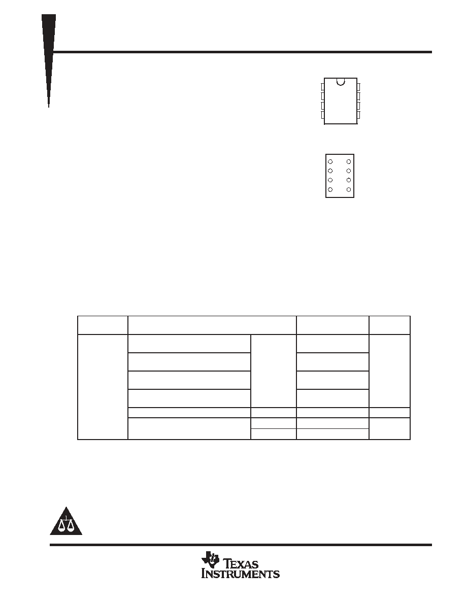
DCT OR DCU PACKAGE
(TOP VIEW)
1
2
3
4
8
7
6
5
1A
3Y
2A
GND
V
CC
1Y
3A
2Y
4
3
2
1
5
6
7
8
GND
2A
3Y
1A
2Y
3A
1Y
V
CC
YEA, YEP, YZA, OR YZP PACKAGE
(BOTTOM VIEW)
PRODUCTION DATA information is current as of publication date.
Products conform to specifications per the terms of Texas Instruments
standard warranty. Production processing does not necessarily include
testing of all parameters.
SN74LVC3G06
TRIPLE INVERTER BUFFER/DRIVER
WITH OPEN DRAIN OUTPUTS
SCES364G- AUGUST 2001 - REVISED AUGUST 2003
2
POST OFFICE BOX 655303
∑
DALLAS, TEXAS 75265
description/ordering information (continued)
The output of the SN74LVC3G06 is open drain and can be connected to other open-drain outputs to implement
active-low wired-OR or active-high wired-AND functions. The maximum sink current is 32 mA.
NanoStar
and NanoFree
package technology is a major breakthrough in IC packaging concepts, using the
die as the package.
This device is fully specified for partial-power-down applications using I
off
. The I
off
circuitry disables the outputs,
preventing damaging current backflow through the device when it is powered down.
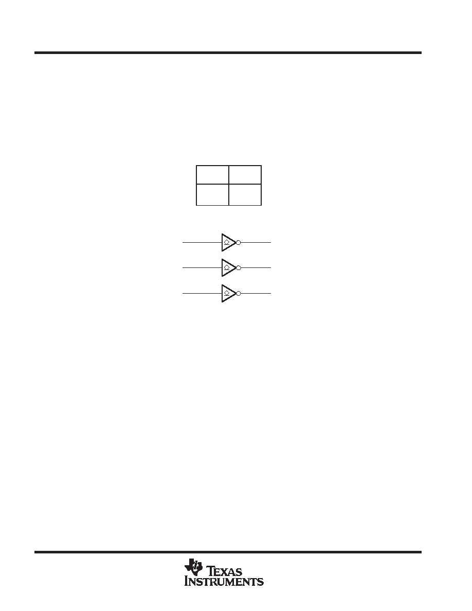
FUNCTION TABLE
(each inverter)
INPUT
A
OUTPUT
Y
H
L
L
H
logic diagram (positive logic)
1A
1Y
1
7
2A
2Y
3
5
3A
3Y
6
2
absolute maximum ratings over operating free-air temperature range (unless otherwise noted)
Supply voltage range, V
CC
-0.5 V to 6.5 V
. . . . . . . . . . . . . . . . . . . . . . . . . . . . . . . . . . . . . . . . . . . . . . . . . . . . . . . . .
Input voltage range, V
I
(see Note 1)
-0.5 V to 6.5 V
. . . . . . . . . . . . . . . . . . . . . . . . . . . . . . . . . . . . . . . . . . . . . . . . .
Voltage range applied to any output in the high-impedance or power-off state, V
O
(see Note 1)
-0.5 V to 6.5 V
. . . . . . . . . . . . . . . . . . . . . . . . . . . . . . . . . . . . . . . . . . . . . . . . . . . . . . . . . . . . . . . . . . .
Voltage range applied to any output in the high or low state, V
O
(see Notes 1 and 2)
-0.5 V to 6.5 V
. . . . . . . . . . . . . . . . . . . . . . . . . . . . . . . . . . . . . . . . . . . . . . . . . . . . . . . . . . . . .
Input clamp current, I
IK
(V
I
< 0)
-50 mA
. . . . . . . . . . . . . . . . . . . . . . . . . . . . . . . . . . . . . . . . . . . . . . . . . . . . . . . . . . .
Output clamp current, I
OK
(V
O
< 0)
-50 mA
. . . . . . . . . . . . . . . . . . . . . . . . . . . . . . . . . . . . . . . . . . . . . . . . . . . . . . . .
Continuous output current, I
O
±
50 mA
. . . . . . . . . . . . . . . . . . . . . . . . . . . . . . . . . . . . . . . . . . . . . . . . . . . . . . . . . . . . .
Continuous current through V
CC
or GND
±
100 mA
. . . . . . . . . . . . . . . . . . . . . . . . . . . . . . . . . . . . . . . . . . . . . . . . . .
Package thermal impedance,
JA
(see Note 3): DCT package
220
∞
C/W
. . . . . . . . . . . . . . . . . . . . . . . . . . . . . . .
DCU package
227
∞
C/W
. . . . . . . . . . . . . . . . . . . . . . . . . . . . . . .
YEA/YZA package
140
∞
C/W
. . . . . . . . . . . . . . . . . . . . . . . . . . .
YEP/YZP package
102
∞
C/W
. . . . . . . . . . . . . . . . . . . . . . . . . . .
Storage temperature range, T
stg
-65
∞
C to 150
∞
C
. . . . . . . . . . . . . . . . . . . . . . . . . . . . . . . . . . . . . . . . . . . . . . . . . . .
Stresses beyond those listed under "absolute maximum ratings" may cause permanent damage to the device. These are stress ratings only, and
functional operation of the device at these or any other conditions beyond those indicated under "recommended operating conditions" is not
implied. Exposure to absolute-maximum-rated conditions for extended periods may affect device reliability.
NOTES:
1. The input negative-voltage and output voltage ratings may be exceeded if the input and output current ratings are observed.
2. The value of VCC is provided in the recommended operating conditions table.
3. The package thermal impedance is calculated in accordance with JESD 51-7.
SN74LVC3G06
TRIPLE INVERTER BUFFER/DRIVER
WITH OPEN DRAIN OUTPUTS
SCES364G- AUGUST 2001 - REVISED AUGUST 2003
3
POST OFFICE BOX 655303
∑
DALLAS, TEXAS 75265
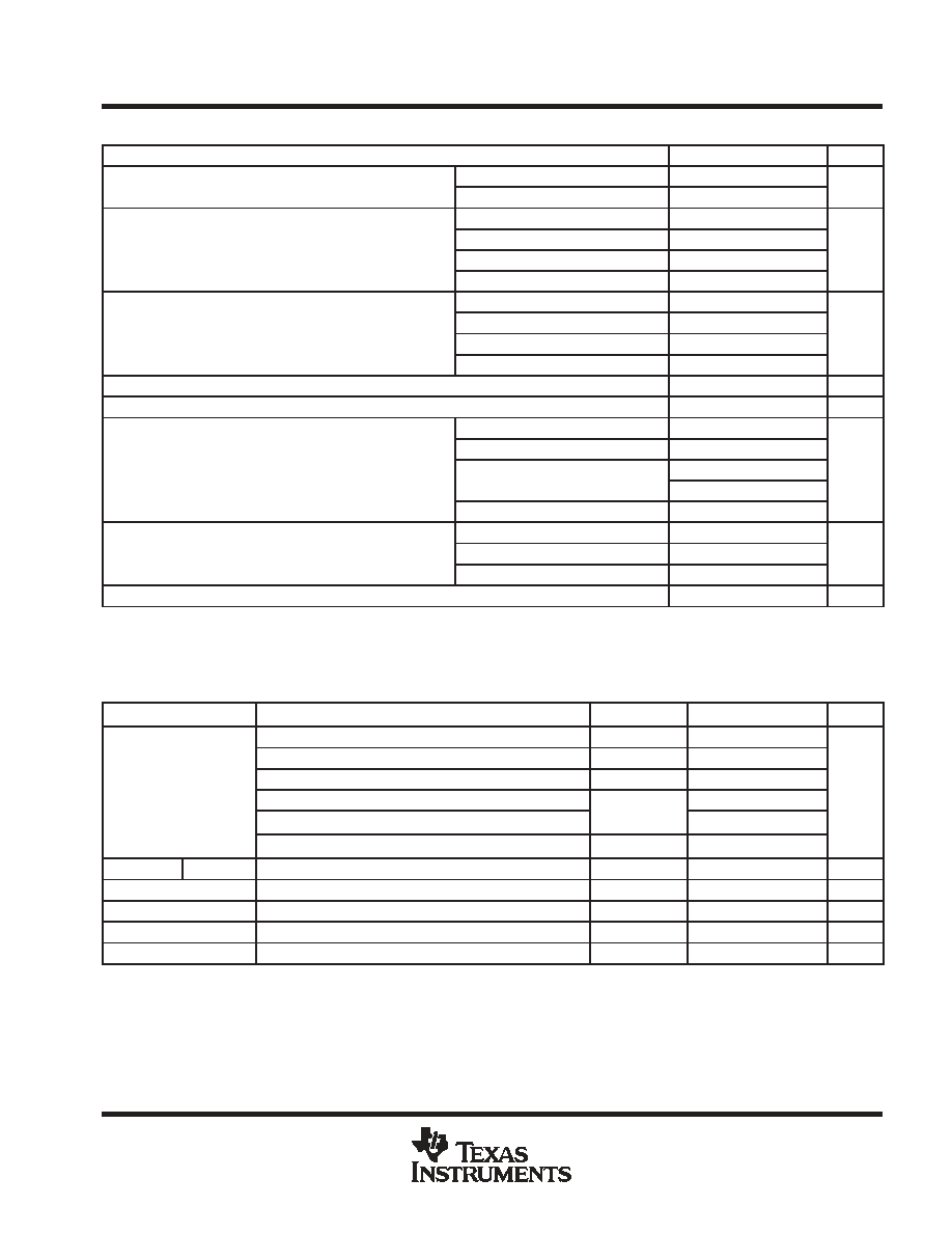
recommended operating conditions (see Note 4)
MIN
MAX
UNIT
VCC
Supply voltage
Operating
1.65
5.5
V
VCC
Supply voltage
Data retention only
1.5
V
VCC = 1.65 V to 1.95 V
0.65
◊
VCC
VIH
High-level input voltage
VCC = 2.3 V to 2.7 V
1.7
V
VIH
High-level input voltage
VCC = 3 V to 3.6 V
2
V
VCC = 4.5 V to 5.5 V
0.7
◊
VCC
VCC = 1.65 V to 1.95 V
0.35
◊
VCC
VIL
Low-level input voltage
VCC = 2.3 V to 2.7 V
0.7
V
VIL
Low-level input voltage
VCC = 3 V to 3.6 V
0.8
V
VCC = 4.5 V to 5.5 V
0.3
◊
VCC
VI
Input voltage
0
5.5
V
VO
Output voltage
0
5.5
V
VCC = 1.65 V
4
VCC = 2.3 V
8
IOL
Low-level output current
VCC = 3 V
16
mA
IOL
Low-level output current
VCC = 3 V
24
mA
VCC = 4.5 V
32
VCC = 1.8 V
±
0.15 V, 2.5 V
±
0.2 V
20
t/
v
Input transition rise or fall rate
VCC = 3.3 V
±
0.3 V
10
ns/V
t/
v
Input transition rise or fall rate
VCC = 5 V
±
0.5 V
5
ns/V
TA
Operating free-air temperature
-40
85
∞
C
NOTE 4: All unused inputs of the device must be held at VCC or GND to ensure proper device operation. Refer to the TI application report,
Implications of Slow or Floating CMOS Inputs, literature number SCBA004.
electrical characteristics over recommended operating free-air temperature range (unless
otherwise noted)
PARAMETER
TEST CONDITIONS
VCC
MIN
TYP
MAX
UNIT
IOL = 100
m
A
1.65 V to 5.5 V
0.1
IOL = 4 mA
1.65 V
0.45
V
IOL = 8 mA
2.3 V
0.3
V
VOL
IOL = 16 mA
3 V
0.4
V
IOL = 24 mA
3 V
0.55
IOL = 32 mA
4.5 V
0.55
II
A inputs
VI = 5.5 V or GND
0 to 5.5 V
±
5
m
A
Ioff
VI or VO = 5.5 V
0
±
10
m
A
ICC
VI = 5.5 V or GND,
IO = 0
1.65 V to 5.5 V
10
m
A
ICC
One input at VCC - 0.6 V,
Other inputs at VCC or GND
3 V to 5.5 V
500
m
A
Ci
VI = VCC or GND
3.3 V
3.5
pF
All typical values are at VCC = 3.3 V, TA = 25
∞
C.
SN74LVC3G06
TRIPLE INVERTER BUFFER/DRIVER
WITH OPEN DRAIN OUTPUTS
SCES364G- AUGUST 2001 - REVISED AUGUST 2003
4
POST OFFICE BOX 655303
∑
DALLAS, TEXAS 75265
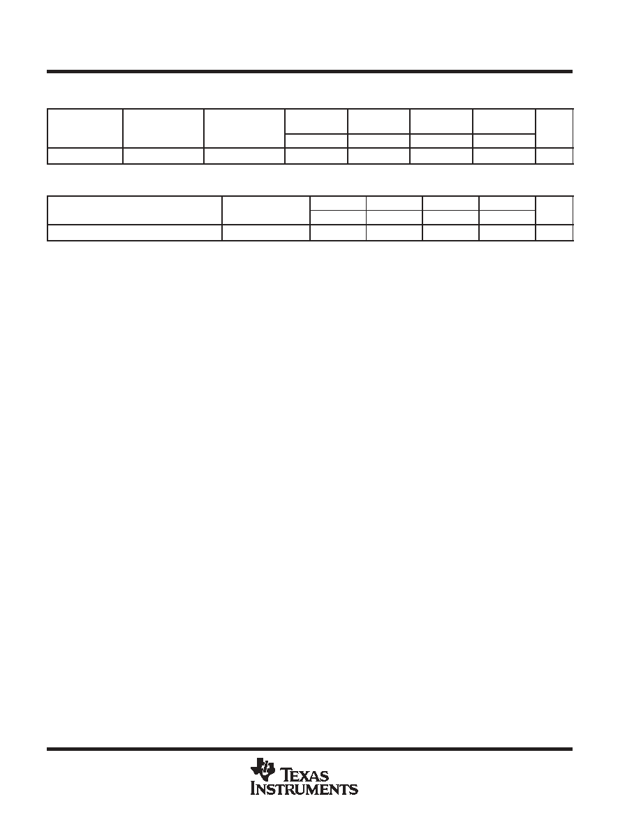
switching characteristics over recommended operating free-air temperature range (unless
otherwise noted) (see Figure 1)
PARAMETER
FROM
(INPUT)
TO
(OUTPUT)
VCC = 1.8 V
±
0.15 V
VCC = 2.5 V
±
0.2 V
VCC = 3.3 V
±
0.3 V
VCC = 5 V
±
0.5 V
UNIT
PARAMETER
(INPUT)
(OUTPUT)
MIN
MAX
MIN
MAX
MIN
MAX
MIN
MAX
UNIT
tpd
A
Y
1.8
7.2
1
3.9
1
3.4
1
2.9
ns
operating characteristics, T
A
= 25
∞
C
PARAMETER
TEST CONDITIONS
VCC = 1.8 V VCC = 2.5 V VCC = 3.3 V
VCC = 5 V
UNIT
PARAMETER
TEST CONDITIONS
TYP
TYP
TYP
TYP
UNIT
Cpd
Power dissipation capacitance
f = 10 MHz
2
2
3
4
pF
SN74LVC3G06
TRIPLE INVERTER BUFFER/DRIVER
WITH OPEN DRAIN OUTPUTS
SCES364G- AUGUST 2001 - REVISED AUGUST 2003
5
POST OFFICE BOX 655303
∑
DALLAS, TEXAS 75265
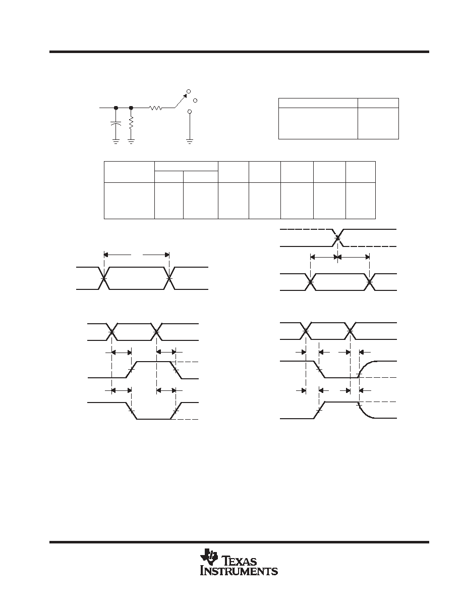
PARAMETER MEASUREMENT INFORMATION
(OPEN DRAIN)
VM
th
tsu
From Output
Under Test
CL
(see Note A)
LOAD CIRCUIT
S1
VLOAD
Open
GND
RL
RL
Data Input
Timing Input
VI
0 V
VI
0 V
0 V
tw
Input
VOLTAGE WAVEFORMS
SETUP AND HOLD TIMES
VOLTAGE WAVEFORMS
PROPAGATION DELAY TIMES
INVERTING AND NONINVERTING OUTPUTS
VOLTAGE WAVEFORMS
PULSE DURATION
tPLH
tPHL
tPHL
tPLH
VOH
VOH
VOL
VOL
VI
0 V
Input
Output
Waveform 1
S1 at VLOAD
(see Note B)
Output
Waveform 2
S1 at VLOAD
(see Note B)
VOL
tPZL
tPZH
tPLZ
tPHZ
VLOAD/2
0 V
VOL + V
VLOAD/2 - V
0 V
VI
VOLTAGE WAVEFORMS
ENABLE AND DISABLE TIMES
LOW- AND HIGH-LEVEL ENABLING
Output
Output
NOTES: A. CL includes probe and jig capacitance.
B. Waveform 1 is for an output with internal conditions such that the output is low except when disabled by the output control.
Waveform 2 is for an output with internal conditions such that the output is high except when disabled by the output control.
C. All input pulses are supplied by generators having the following characteristics: PRR
10 MHz, ZO = 50
.
D. The outputs are measured one at a time with one transition per measurement.
E. Since this device has open-drain outputs, tPLZ and tPZL are the same as tpd.
F. tPZL is measured at VM.
G. tPLZ is measured at VOL + V
.
H. All parameters and waveforms are not applicable to all devices.
Output
Control
VM
VM
VM
VM
VM
VM
VM
VM
VM
VM
VM
VM
VI
VM
VM
1.8 V
±
0.15 V
2.5 V
±
0.2 V
3.3 V
±
0.3 V
5 V
±
0.5 V
1 k
500
500
500
VCC
RL
2
◊
VCC
2
◊
VCC
6 V
2
◊
VCC
VLOAD
CL
30 pF
30 pF
50 pF
50 pF
0.15 V
0.15 V
0.3 V
0.3 V
V
VCC
VCC
3 V
VCC
VI
VCC/2
VCC/2
1.5 V
VCC/2
VM
tr/tf
2 ns
2 ns
2.5 ns
2.5 ns
INPUT
tPZL (see Notes E and F)
tPLZ (see Notes E and G)
tPHZ/tPZH
VLOAD
VLOAD
VLOAD
TEST
S1
VLOAD/2
Figure 1. Load Circuit and Voltage Waveforms