SN74LVCC3245A
OCTAL BUS TRANSCEIVER WITH ADJUSTABLE OUTPUT VOLTAGE
AND 3-STATE OUTPUTS
SCAS585L ≠ NOVEMBER 1996 ≠ REVISED AUGUST 2003
1
POST OFFICE BOX 655303
∑
DALLAS, TEXAS 75265
D
Bidirectional Voltage Translator
D
2.3 V to 3.6 V on A Port and 3 V to 5.5 V on
B Port
D
Latch-Up Performance Exceeds 250 mA Per
JESD 17
D
ESD Protection Exceeds JESD 22
≠ 2000-V Human-Body Model (A114-A)
≠ 200-V Machine Model (A115-A)
≠ 1000-V Charged-Device Model (C101)
description/ordering information
This 8-bit (octal) noninverting bus transceiver
contains two separate supply rails. The B port is
designed to track V
CCB
,
which accepts voltages
from 3 V to 5.5 V, and the A port is designed to
track V
CCA
, which operates at 2.3 V to 3.6 V. This
allows for translation from a 3.3-V to a 5-V system
environment and vice versa, or from a 2.5-V to a
3.3-V system environment and vice versa.
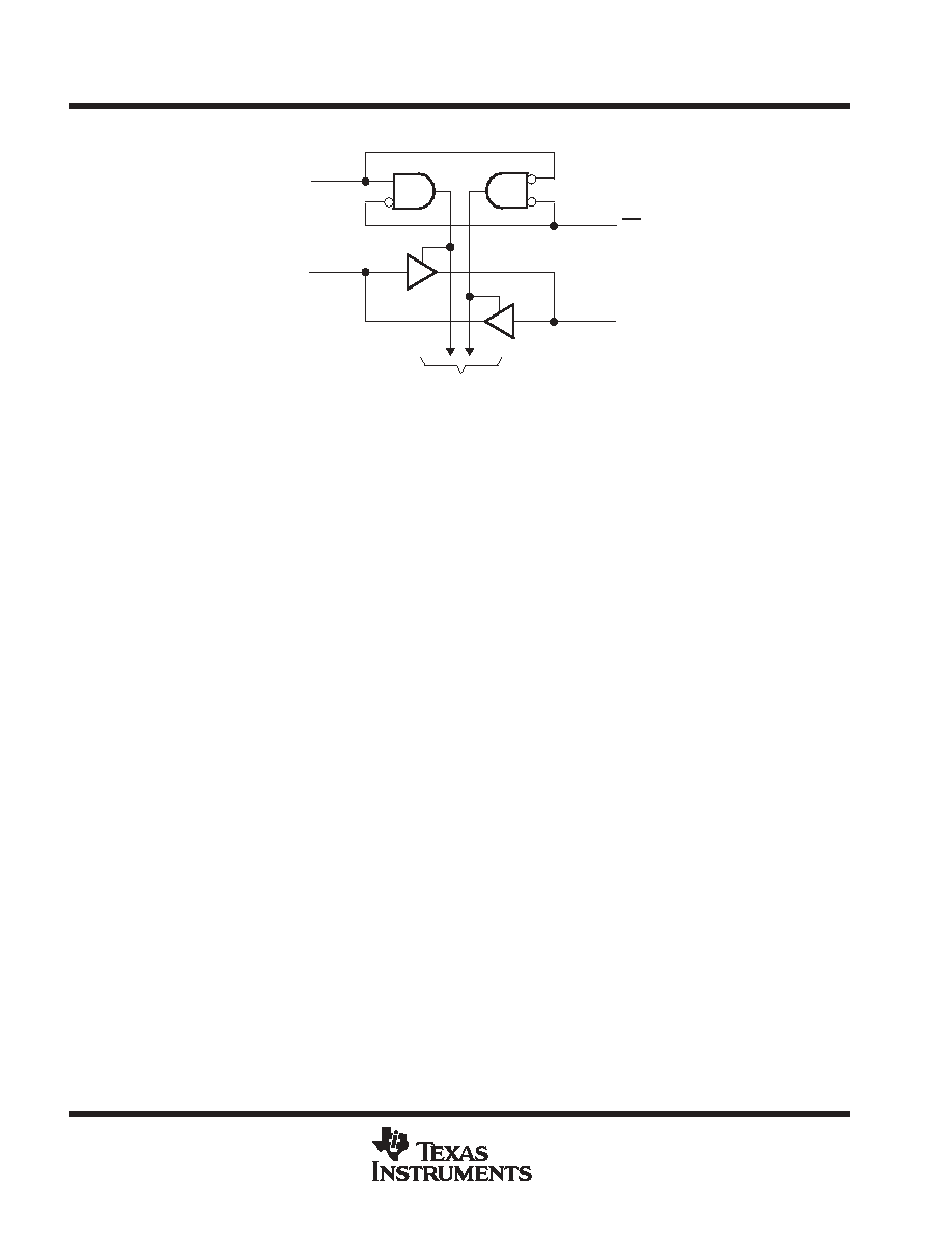
The SN74LVCC3245A is designed for asynchronous communication between data buses. The device
transmits data from the A bus to the B bus or from the B bus to the A bus, depending on the logic level at the
direction-control (DIR) input. The output-enable (OE) input can be used to disable the device so the buses are
effectively isolated.
ORDERING INFORMATION
TA
PACKAGE
ORDERABLE
PART NUMBER
TOP-SIDE
MARKING
≠40 C to 85 C
SOIC ≠ DW
Tube of 25
SN74LVCC3245ADW
LVCC3245A
≠40 C to 85 C
SOIC ≠ DW
Reel of 2000
SN74LVCC3245ADWR
LVCC3245A
≠40 C to 85 C
SOP ≠ NS
Reel of 2000
SN74LVCC3245ANSR
LVCC3245A
≠40
∞
C to 85
∞
C
SSOP ≠ DB
Reel of 2000
SN74LVCC3245ADBR
LH245A
≠40 C to 85 C
TSSOP ≠ PW
Tube of 60
SN74LVCC3245APW
LH245A
TSSOP ≠ PW
Reel of 2000
SN74LVCC3245APWR
LH245A
Reel of 250
SN74LVCC3245APWT
Package drawings, standard packing quantities, thermal data, symbolization, and PCB design
guidelines are available at www.ti.com/sc/package.
FUNCTION TABLE
(each transceiver)
INPUTS
OPERATION
OE
DIR
OPERATION
L
L
B data to A bus
L
H
A data to B bus
H
X
Isolation
Copyright
2003, Texas Instruments Incorporated
PRODUCTION DATA information is current as of publication date.
Products conform to specifications per the terms of Texas Instruments
standard warranty. Production processing does not necessarily include
testing of all parameters.
Please be aware that an important notice concerning availability, standard warranty, and use in critical applications of
Texas Instruments semiconductor products and disclaimers thereto appears at the end of this data sheet.
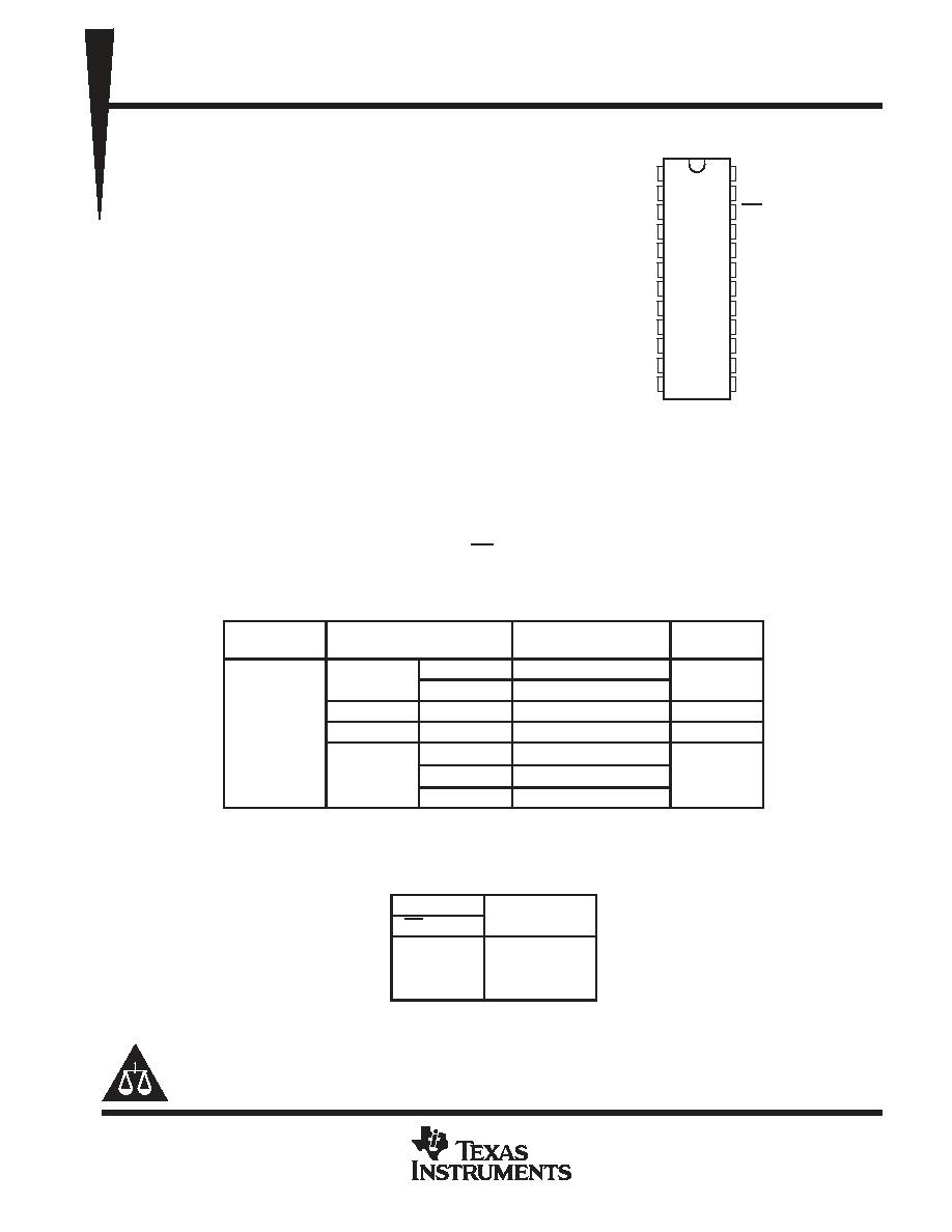
DB, DW, NS, OR PW PACKAGE
(TOP VIEW)
1
2
3
4
5
6
7
8
9
10
11
12
24
23
22
21
20
19
18
17
16
15
14
13
V
CCA
DIR
A1
A2
A3
A4
A5
A6
A7
A8
GND
GND
V
CCB
NC
OE
B1
B2
B3
B4
B5
B6
B7
B8
GND
NC ≠ No internal connection
SN74LVCC3245A
OCTAL BUS TRANSCEIVER WITH ADJUSTABLE OUTPUT VOLTAGE
AND 3-STATE OUTPUTS
SCAS585L ≠ NOVEMBER 1996 ≠ REVISED AUGUST 2003
2
POST OFFICE BOX 655303
∑
DALLAS, TEXAS 75265
logic diagram (positive logic)
DIR
OE
A1
B1
To Seven Other Channels
2
3
22
21
absolute maximum ratings over operating free-air temperature range (unless otherwise noted)
Supply voltage range, V
CCA
and V
CCB
≠0.5 V to 6 V
. . . . . . . . . . . . . . . . . . . . . . . . . . . . . . . . . . . . . . . . . . . . . . .
Input voltage range, V
I
: All A ports (see Note 1)
≠0.5 V to V
CCA
+ 0.5 V
. . . . . . . . . . . . . . . . . . . . . . . . . . . . . .
All B ports (see Note 2)
≠0.5 V to V
CCB
+ 0.5 V
. . . . . . . . . . . . . . . . . . . . . . . . . . . . . .
Except I/O ports (see Note 1)
≠0.5 V to V
CCA
+ 0.5 V
. . . . . . . . . . . . . . . . . . . . . . . . .
Output voltage range, V
O
(see Note 2): All A ports
≠0.5 V to V
CCA
+ 0.5 V
. . . . . . . . . . . . . . . . . . . . . . . . . . . .
All B ports
≠0.5 V to V
CCB
+ 0.5 V
. . . . . . . . . . . . . . . . . . . . . . . . . . . .
Input clamp current, I
IK
(V
I
< 0)
≠50 mA
. . . . . . . . . . . . . . . . . . . . . . . . . . . . . . . . . . . . . . . . . . . . . . . . . . . . . . . . . . .
Output clamp current, I
OK
(V
O
< 0)
≠50 mA
. . . . . . . . . . . . . . . . . . . . . . . . . . . . . . . . . . . . . . . . . . . . . . . . . . . . . . . .
Continuous output current, I
O
±
50 mA
. . . . . . . . . . . . . . . . . . . . . . . . . . . . . . . . . . . . . . . . . . . . . . . . . . . . . . . . . . . . .
Continuous current through V
CCA
, V
CCB
, or GND
±
100 mA
. . . . . . . . . . . . . . . . . . . . . . . . . . . . . . . . . . . . . . . . .
Package thermal impedance,
JA
(see Note 3): DB package
63
∞
C/W
. . . . . . . . . . . . . . . . . . . . . . . . . . . . . . . . .
DW package
46
∞
C/W
. . . . . . . . . . . . . . . . . . . . . . . . . . . . . . . . .
NS package
65
∞
C/W
. . . . . . . . . . . . . . . . . . . . . . . . . . . . . . . . .
PW package
88
∞
C/W
. . . . . . . . . . . . . . . . . . . . . . . . . . . . . . . . .
Storage temperature range, T
stg
≠65
∞
C to 150
∞
C
. . . . . . . . . . . . . . . . . . . . . . . . . . . . . . . . . . . . . . . . . . . . . . . . . . .
Stresses beyond those listed under "absolute maximum ratings" may cause permanent damage to the device. These are stress ratings only, and
functional operation of the device at these or any other conditions beyond those indicated under "recommended operating conditions" is not
implied. Exposure to absolute-maximum-rated conditions for extended periods may affect device reliability.
NOTES:
1. This value is limited to 4.6 V maximum.
2. This value is limited to 6 V maximum.
3. The package thermal impedance is calculated in accordance with JESD 51-7.
SN74LVCC3245A
OCTAL BUS TRANSCEIVER WITH ADJUSTABLE OUTPUT VOLTAGE
AND 3-STATE OUTPUTS
SCAS585L ≠ NOVEMBER 1996 ≠ REVISED AUGUST 2003
3
POST OFFICE BOX 655303
∑
DALLAS, TEXAS 75265
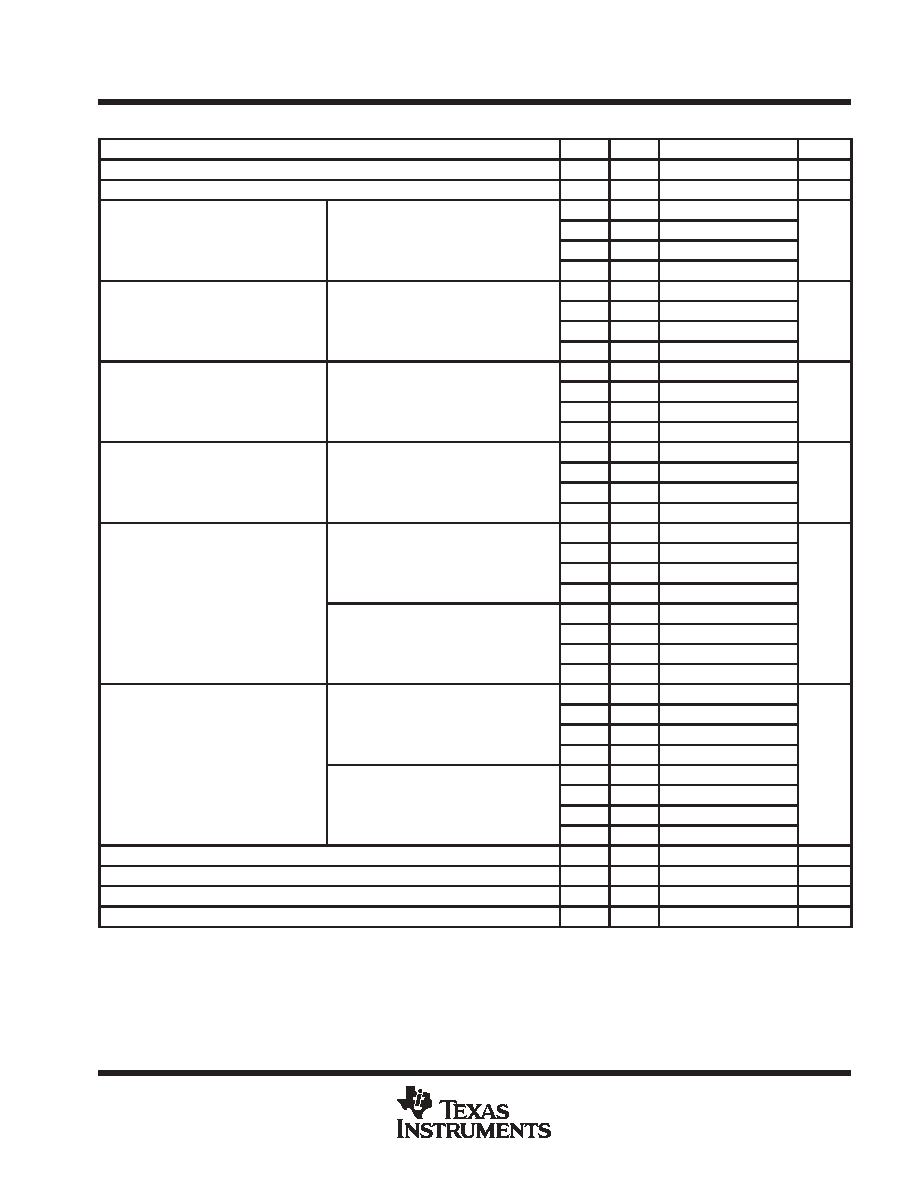
recommended operating conditions (see Note 4)
VCCA
VCCB
MIN
NOM
MAX
UNIT
VCCA
Supply voltage
2.3
3.3
3.6
V
VCCB
Supply voltage
3
5
5.5
V
V
High-level input voltage
V
0.1 V or V
V
≠ 0.1 V
2.3 V
3 V
1.7
V
VIHA
High-level input voltage
VOB
0.1 V or VOB
VCCB ≠ 0.1 V
2.7 V
3 V
2
V
VIHA
High-level input voltage
VOB
0.1 V or VOB
VCCB ≠ 0.1 V
3 V
3.6 V
2
V
3.6 V
5.5 V
2
V
High-level input voltage
V
0.1 V or V
V
≠ 0.1 V
2.3 V
3 V
2
V
VIHB
High-level input voltage
VOA
0.1 V or VOA
VCCA ≠ 0.1 V
2.7 V
3 V
2
V
VIHB
High-level input voltage
VOA
0.1 V or VOA
VCCA ≠ 0.1 V
3 V
3.6 V
2
V
3.6 V
5.5 V
3.85
V
Low-level input voltage
V
0.1 V or V
V
≠ 0.1 V
2.3 V
3 V
0.7
V
VILA
Low-level input voltage
VOB
0.1 V or VOB
VCCB ≠ 0.1 V
2.7 V
3 V
0.8
V
VILA
Low-level input voltage
VOB
0.1 V or VOB
VCCB ≠ 0.1 V
3 V
3.6 V
0.8
V
3.6 V
5.5 V
0.8
V
Low-level input voltage
V
0.1 V or V
V
≠ 0.1 V
2.3 V
3 V
0.8
V
VILB
Low-level input voltage
VOA
0.1 V or VOA
VCCA ≠ 0.1 V
2.7 V
3 V
0.8
V
VILB
Low-level input voltage
VOA
0.1 V or VOA
VCCA ≠ 0.1 V
3 V
3.6 V
0.8
V
3.6 V
5.5 V
1.65
V
High-level input voltage
V
0.1 V or V
V
≠ 0.1 V
2.3 V
3 V
1.7
V
V
High-level input voltage
VOB
0.1 V or VOB
VCCB ≠ 0.1 V
2.7 V
3 V
2
V
V
High-level input voltage
VOB
0.1 V or VOB
VCCB ≠ 0.1 V
3 V
3.6 V
2
V
VIH
High-level input voltage
3.6 V
5.5 V
2
V
VIH
High-level input voltage
(control pins)
V
0.1 V or V
V
≠ 0.1 V
2.3 V
3 V
2
V
VOA
0.1 V or VOA
VCCA ≠ 0.1 V
2.7 V
3 V
2
VOA
0.1 V or VOA
VCCA ≠ 0.1 V
3 V
3.6 V
2
3.6 V
5.5 V
2
V
Low-level input voltage
V
0.1 V or V
V
≠ 0.1 V
2.3 V
3 V
0.7
V
V
Low-level input voltage
VOB
0.1 V or VOB
VCCB ≠ 0.1 V
2.7 V
3 V
0.8
V
V
Low-level input voltage
VOB
0.1 V or VOB
VCCB ≠ 0.1 V
3 V
3.6 V
0.8
V
VIL
Low-level input voltage
3.6 V
5.5 V
0.8
V
VIL
Low-level input voltage
(control pins)
V
0.1 V or V
V
≠ 0.1 V
2.3 V
3 V
0.8
V
VOA
0.1 V or VOA
VCCA ≠ 0.1 V
2.7 V
3 V
0.8
VOA
0.1 V or VOA
VCCA ≠ 0.1 V
3 V
3.6 V
0.8
3.6 V
5.5 V
0.8
VIA
Input voltage
0
VCCA
V
VIB
Input voltage
0
VCCB
V
VOA
Output voltage
0
VCCA
V
VOB
Output voltage
0
VCCB
V
NOTE 4: All unused inputs of the device must be held at the associated VCC or GND to ensure proper device operation. Refer to the TI application
report, Implications of Slow or Floating CMOS Inputs, literature number SCBA004.
SN74LVCC3245A
OCTAL BUS TRANSCEIVER WITH ADJUSTABLE OUTPUT VOLTAGE
AND 3-STATE OUTPUTS
SCAS585L ≠ NOVEMBER 1996 ≠ REVISED AUGUST 2003
4
POST OFFICE BOX 655303
∑
DALLAS, TEXAS 75265
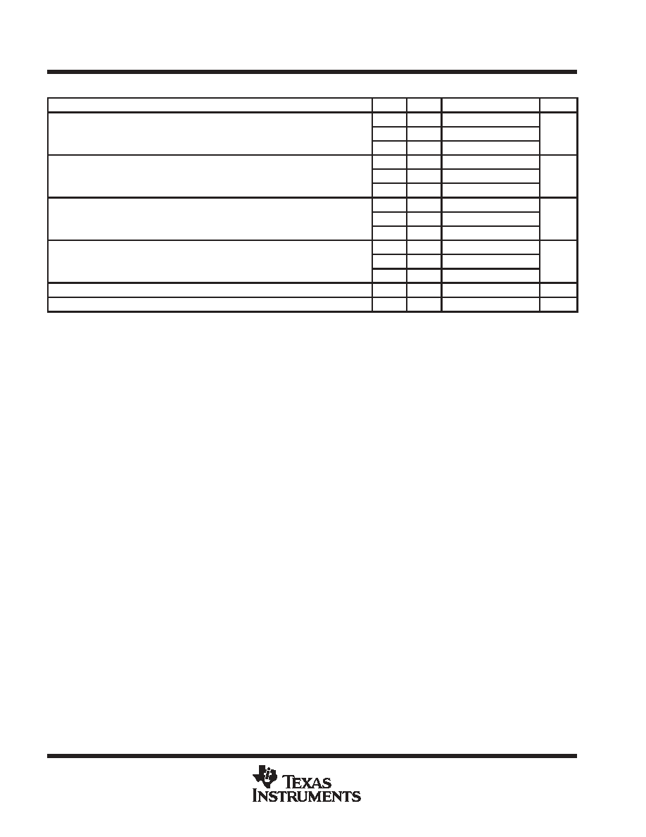
recommended operating conditions (see Note 4) (continued)
VCCA
VCCB
MIN
NOM
MAX
UNIT
I
High-level output current
2.3 V
3 V
≠8
mA
IOHA
High-level output current
2.7 V
3 V
≠12
mA
OHA
3.3 V
3 V
≠24
I
High-level output current
2.3 V
3.3 V
≠12
mA
IOHB
High-level output current
2.7 V
3.3 V
≠12
mA
OHB
3.3 V
3 V
≠24
I
Low-level output current
2.3 V
3 V
8
mA
IOLA
Low-level output current
2.7 V
3 V
12
mA
OLA
3.3 V
3 V
24
I
Low-level output current
2.3 V
3.3 V
12
mA
IOLB
Low-level output current
2.7 V
3.3 V
12
mA
OLB
3.3 V
3 V
24
t/
v
Input transition rise or fall rate
10
ns/V
TA
Operating free-air temperature
≠40
85
∞
C
NOTE 4: All unused inputs of the device must be held at the associated VCC or GND to ensure proper device operation. Refer to the TI application
report, Implications of Slow or Floating CMOS Inputs, literature number SCBA004.
SN74LVCC3245A
OCTAL BUS TRANSCEIVER WITH ADJUSTABLE OUTPUT VOLTAGE
AND 3-STATE OUTPUTS
SCAS585L ≠ NOVEMBER 1996 ≠ REVISED AUGUST 2003
5
POST OFFICE BOX 655303
∑
DALLAS, TEXAS 75265
electrical characteristics over recommended operating free-air temperature range (unless
otherwise noted)
PARAMETER
TEST CONDITIONS
VCCA
VCCB
MIN
TYP
MAX
UNIT
V
IOH = ≠100
µ
A
3 V
3 V
2.9
3
V
V
IOH = ≠8 mA
2.3 V
3 V
2
V
VOHA
IOH = ≠12 mA
2.7 V
3 V
2.2
2.5
V
VOHA
IOH = ≠12 mA
3 V
3 V
2.4
2.8
V
IOH = ≠24 mA
3 V
3 V
2.2
2.6
IOH = ≠24 mA
2.7 V
4.5 V
2
2.3
V
IOH = ≠100
µ
A
3 V
3 V
2.9
3
V
V
IOH = ≠12 mA
2.3 V
3 V
2.4
V
VOHB
IOH = ≠12 mA
2.7 V
3 V
2.4
2.8
V
OHB
IOH = ≠24 mA
3 V
3 V
2.2
2.6
IOH = ≠24 mA
2.7 V
4.5 V
3.2
4.2
V
IOL = 100
µ
A
3 V
3 V
0.1
V
V
IOL = 8 mA
2.3 V
3 V
0.6
V
VOLA
IOL = 12 mA
2.7 V
3 V
0.1
0.5
V
OLA
IOL = 24 mA
3 V
3 V
0.2
0.5
IOL = 24 mA
2.7 V
4.5 V
0.2
0.5
V
IOL = 100
µ
A
3 V
3 V
0.1
V
VOLB
IOL = 12 mA
2.3 V
3 V
0.4
V
VOLB
IOL = 24 mA
3 V
3 V
0.2
0.5
V
IOL = 24 mA
3 V
4.5 V
0.2
0.5
II
Control inputs
VI = VCCA or GND
3.6 V
3.6 V
±
0.1
±
1
µ
A
II
Control inputs
VI = VCCA or GND
3.6 V
5.5 V
±
0.1
±
1
µ
A
IOZ
A or B ports
VO = VCCA/B or GND,
VI = VIL or VIH
3.6 V
3.6 V
±
0.5
±
5
µ
A
I
B to A
A port = VCCA or GND,
IO = 0
3.6 V
Open
5
50
A
ICCA
B to A
B port = VCCB or GND,
IO = 0
3.6 V
3.6 V
5
50
µ
A
CCA
B port = VCCB or GND,
IO = 0
3.6 V
5.5 V
5
50
ICCB
A to B
A port = VCCA or GND,
IO = 0
3.6 V
3.6 V
5
50
µ
A
ICCB
A to B
A port = VCCA or GND,
IO = 0
3.6 V
5.5 V
8
80
µ
A
A port
VI = VCCA ≠ 0.6 V, Other inputs at VCCA or GND,
OE at GND and DIR at VCCA
3.6 V
3.6 V
0.35
0.5
mA
ICCA
OE
VI = VCCA ≠ 0.6 V, Other inputs at VCCA or GND,
DIR at VCCA
3.6 V
3.6 V
0.35
0.5
mA
DIR
VI = VCCA ≠ 0.6 V, Other inputs at VCCA or GND,
OE at GND
3.6 V
3.6 V
0.35
0.5
ICCB
B port
VI = VCCB ≠ 2.1 V, Other inputs at VCCB or GND,
OE at GND and DIR at GND
3.6 V
5.5 V
1
1.5
mA
Ci
Control inputs
VI = VCCA or GND
Open
Open
4
pF
Cio
A or B ports
VO = VCCA/B or GND
3.3 V
5 V
18.5
pF
For I/O ports, the parameter IOZ includes the input leakage current.
This is the increase in supply current for each input that is at one of the specified voltage levels, rather than 0 V or the associated VCC.