www.ti.com
FEATURES
DESCRIPTION/ORDERING INFORMATION
SN74LVCH322244A
32-BIT BUFFER/DRIVER
WITH 3-STATE OUTPUTS
SCES405B ≠ JULY 2002 ≠ REVISED APRIL 2005
∑
I
off
Supports Partial-Power-Down Mode
Operation
∑
Member of the Texas Instruments Widebus+TM
Family
∑
Supports Mixed-Mode Signal Operation
On All Ports (5-V Input/Output Voltage With
∑
Operates From 1.65 V to 3.6 V
3.3-V V
CC
)
∑
Inputs Accept Voltages to 5.5 V
∑
Bus Hold on Data Inputs Eliminates the
∑
Max t
pd
of 4.4 ns at 3.3 V
Need for External Pullup/Pulldown
∑
Output Ports Have Equivalent 26-
Series
Resistors
Resistors, So No External Resistors Are
∑
Latch-Up Performance Exceeds 100 mA
Required
Per JESD 78, Class II
∑
Typical V
OLP
(Output Ground Bounce)
∑
ESD Protection Exceeds JESD 22
< 0.8 V at V
CC
= 3.3 V, T
A
= 25∞C
≠ 2000-V Human-Body Model (A114-A)
∑
Typical V
OHV
(Output V
OH
Undershoot)
≠ 200-V Machine Model (A115-A)
> 2 V at V
CC
= 3.3 V, T
A
= 25∞C
≠ 1000-V Charged-Device Model (C101)
This 32-bit buffer/driver is designed for 1.65-V to 3.6-V V
CC
operation.
The SN74LVCH322244A is designed specifically to improve the performance and density of 3-state memory
address drivers, clock drivers, and bus-oriented receivers and transmitters.
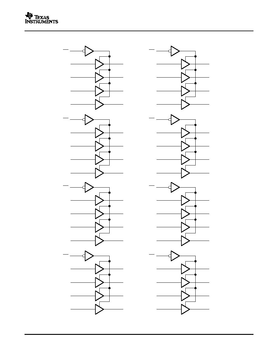
The device can be used as eight 4-bit buffers, four 8-bit buffers, two 16-bit buffers, or one 32-bit buffer. It
provides true outputs and symmetrical active-low output-enable (OE) inputs.
Inputs can be driven from either 3.3-V or 5-V devices. This feature allows the use of these devices as translators
in a mixed 3.3-V/5-V system environment.
The outputs, which are designed to sink up to 12 mA, include equivalent 26-
resistors to reduce overshoot and
undershoot.
To ensure the high-impedance state during power up or power down, OE should be tied to V
CC
through a pullup
resistor; the minimum value of the resistor is determined by the current-sinking capability of the driver.
Active bus-hold circuitry holds unused or undriven inputs at a valid logic state. Use of pullup or pulldown resistors
with the bus-hold circuitry is not recommended.
This device is fully specified for partial-power-down applications using I
off
. The I
off
circuitry disables the outputs,
preventing damaging current backflow through the device when it is powered down.
ORDERING INFORMATION
T
A
PACKAGE
(1)
ORDERABLE PART NUMBER
TOP-SIDE MARKING
LFBGA ≠ GKE
SN74LVCH322244AKR
≠40∞C to 85∞C
Tape and reel
CG244A
LFBGA ≠ ZKE (Pb-free)
74LVCH322244AZKER
(1)
Package drawings, standard packing quantities, thermal data, symbolization, and PCB design guidelines are available at
www.ti.com/sc/package.
FUNCTION TABLE
(EACH 4-BIT BUFFER)
INPUTS
OUTPUT
Y
OE
A
L
H
H
L
L
L
H
X
Z
Please be aware that an important notice concerning availability, standard warranty, and use in critical applications of Texas
Instruments semiconductor products and disclaimers thereto appears at the end of this data sheet.
Widebus+ is a trademark of Texas Instruments.
PRODUCTION DATA information is current as of publication date.
Copyright © 2002≠2005, Texas Instruments Incorporated
Products conform to specifications per the terms of the Texas
Instruments standard warranty. Production processing does not
necessarily include testing of all parameters.

www.ti.com
Absolute Maximum Ratings
(1)
Recommended Operating Conditions
(1)
SN74LVCH322244A
32-BIT BUFFER/DRIVER
WITH 3-STATE OUTPUTS
SCES405B ≠ JULY 2002 ≠ REVISED APRIL 2005
over operating free-air temperature range (unless otherwise noted)
MIN
MAX
UNIT
V
CC
Supply voltage range
≠0.5
6.5
V
V
I
Input voltage range
(2)
≠0.5
6.5
V
V
O
Voltage range applied to any output in the high-impedance or power-off state
(2)
≠0.5
6.5
V
V
O
Voltage range applied to any output in the high or low state
(2) (3)
≠0.5 V
CC
+ 0.5
V
I
IK
Input clamp current
V
I
< 0
≠50
mA
I
OK
Output clamp current
V
O
< 0
≠50
mA
I
O
Continuous output current
±50
mA
Continuous current through each V
CC
or GND
±100
mA
JA
Package thermal impedance
(4)
GKE/ZKE package
40
∞C/W
T
stg
Storage temperature range
≠65
150
∞C
(1)
Stresses beyond those listed under "absolute maximum ratings" may cause permanent damage to the device. These are stress ratings
only, and functional operation of the device at these or any other conditions beyond those indicated under "recommended operating
conditions" is not implied. Exposure to absolute-maximum-rated conditions for extended periods may affect device reliability.
(2)
The input negative-voltage and output voltage ratings may be exceeded if the input and output current ratings are observed.
(3)
The value of V
CC
is provided in the recommended operating conditions table.
(4)
The package thermal impedance is calculated in accordance with JESD 51-7.
MIN
MAX
UNIT
Operating
1.65
3.6
V
CC
Supply voltage
V
Data retention only
1.5
V
CC
= 1.65 V to 1.95 V
0.65 ◊ V
CC
V
IH
High-level input voltage
V
CC
= 2.3 V to 2.7 V
1.7
V
V
CC
= 2.7 V to 3.6 V
2
V
CC
= 1.65 V to 1.95 V
0.35 ◊ V
CC
V
IL
Low-level input voltage
V
CC
= 2.3 V to 2.7 V
0.7
V
V
CC
= 2.7 V to 3.6 V
0.8
V
I
Input voltage
0
5.5
V
High or low state
0
V
CC
V
O
Output voltage
V
3-state
0
5.5
V
CC
= 1.65 V
≠2
V
CC
= 2.3 V
≠4
I
OH
High-level output current
mA
V
CC
= 2.7 V
≠8
V
CC
= 3 V
≠12
V
CC
= 1.65 V
2
V
CC
= 2.3 V
4
I
OL
Low-level output current
mA
V
CC
= 2.7 V
8
V
CC
= 3 V
12
t/
v
Input transition rise or fall rate
10
ns/V
T
A
Operating free-air temperature
≠40
85
∞C
(1)
All unused control inputs of the device must be held at V
CC
or GND to ensure proper device operation. Refer to the TI application report,
Implications of Slow or Floating CMOS Inputs, literature number SCBA004.
4

www.ti.com
Electrical Characteristics
Switching Characteristics
SN74LVCH322244A
32-BIT BUFFER/DRIVER
WITH 3-STATE OUTPUTS
SCES405B ≠ JULY 2002 ≠ REVISED APRIL 2005
over recommended operating free-air temperature range (unless otherwise noted)
PARAMETER
TEST CONDITIONS
V
CC
MIN
TYP
(1)
MAX
UNIT
I
OH
= ≠100
µ
A
1.65 V to 3.6 V
V
CC
≠ 0.2
I
OH
= ≠2 mA
1.65 V
1.2
2.3 V
1.7
I
OH
= ≠4 mA
V
OH
2.7 V
2.2
V
I
OH
= ≠6 mA
3 V
2.4
I
OH
= ≠8 mA
2.7 V
2
I
OH
= ≠12 mA
3 V
2
I
OL
= 100
µ
A
1.65 V to 3.6 V
0.2
I
OL
= 2 mA
1.65 V
0.45
2.3 V
0.7
I
OL
= 4 mA
V
OL
2.7 V
0.4
V
I
OL
= 6 mA
3 V
0.55
I
OL
= 8 mA
2.7 V
0.6
I
OL
= 12 mA
3 V
0.8
I
I
V
I
= 0 to 5.5 V
3.6 V
±5
µ
A
V
I
= 0.58 V
(2)
1.65 V
V
I
= 1.07 V
(2)
V
I
= 0.7 V
45
2.3 V
I
I(hold)
V
I
= 1.7 V
≠45
µ
A
V
I
= 0.8 V
75
3 V
V
I
= 2 V
≠75
V
I
= 0 to 3.6 V
(3)
3.6 V
±500
I
off
V
I
or V
O
= 5.5 V
0
±10
µ
A
I
OZ
V
O
= 0 to 5.5 V
3.6 V
±10
µ
A
V
I
= V
CC
or GND
40
I
CC
I
O
= 0
3.6 V
µ
A
3.6 V
V
I
5.5 V
(4)
40
I
CC
One input at V
CC
≠ 0.6 V,
Other inputs at V
CC
or GND
2.7 V to 3.6 V
500
µ
A
C
i
V
I
= V
CC
or GND
3.3 V
5.5
pF
C
o
V
O
= V
CC
or GND
3.3 V
6
pF
(1)
All typical values are at V
CC
= 3.3 V, T
A
= 25∞C.
(2)
This information was not available at the time of publication.
(3)
This is the bus-hold maximum dynamic current. It is the minimum overdrive current required to switch the input from one state to
another.
(4)
This applies in the disabled state only.
over recommended operating free-air temperature range (unless otherwise noted) (see
Figure 1
)
V
CC
= 1.8 V
V
CC
= 2.5 V
V
CC
= 3.3 V
V
CC
= 2.7 V
FROM
TO
± 0.15 V
± 0.2 V
± 0.3 V
PARAMETER
UNIT
(INPUT)
(OUTPUT)
MIN
MAX
MIN
MAX
MIN
MAX
MIN
MAX
t
pd
A
Y
(1)
(1)
(1)
(1)
1
5.6
1.1
4.4
ns
t
en
OE
Y
(1)
(1)
(1)
(1)
1
6.9
1
5.5
ns
t
dis
OE
Y
(1)
(1)
(1)
(1)
1
6.8
1.8
6.3
ns
(1)
This information was not available at the time of publication.
5