www.ti.com
FEATURES
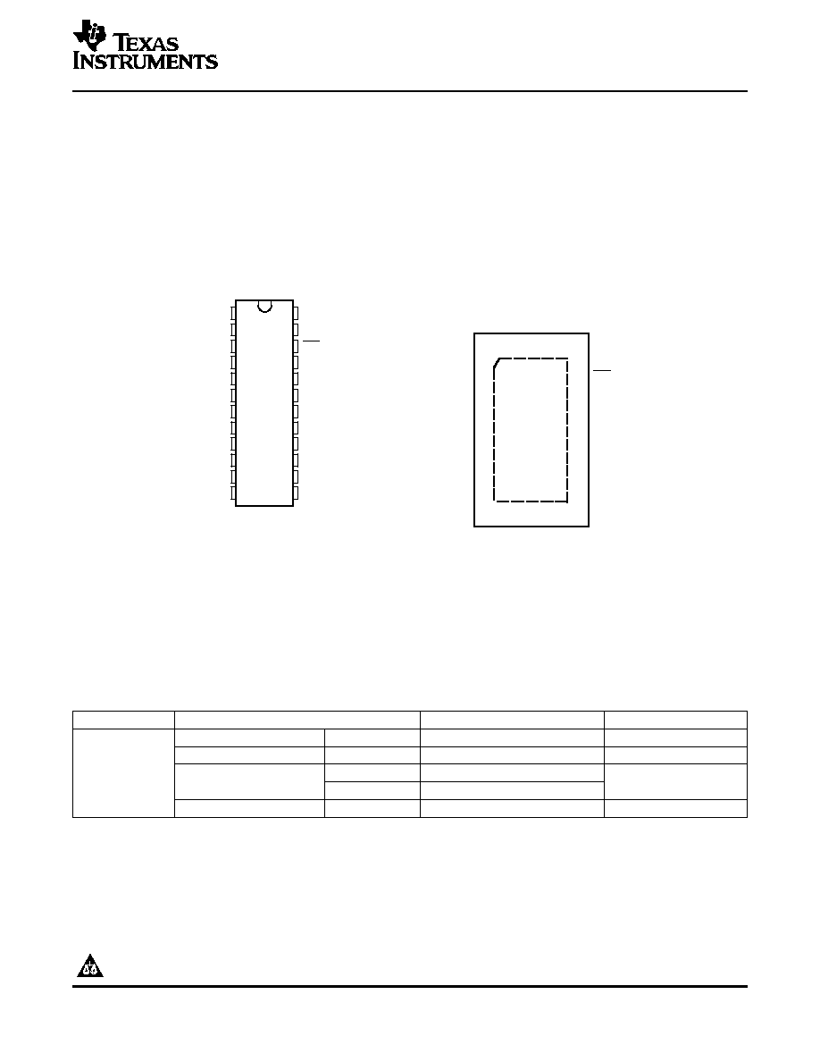
DB, DGV, OR PW PACKAGE
(TOP VIEW)
1
2
3
4
5
6
7
8
9
10
11
12
24
23
22
21
20
19
18
17
16
15
14
13
V
CCA
DIR
A1
A2
A3
A4
A5
A6
A7
A8
GND
GND
V
CCB
V
CCB
OE
B1
B2
B3
B4
B5
B6
B7
B8
GND
RHL PACKAGE
(TOP VIEW)
1
24
12
13
2
3
4
5
6
7
8
9
10
11
23
22
21
20
19
18
17
16
15
14
V
CCB
OE
B1
B2
B3
B4
B5
B6
B7
B8
DIR
A1
A2
A3
A4
A5
A6
A7
A8
GND
GND
V
GND
CCB
V
CCA
DESCRIPTION/ORDERING INFORMATION
SN74LVCH8T245
8-BIT DUAL-SUPPLY BUS TRANSCEIVER
WITH CONFIGURABLE VOLTAGE TRANSLATION AND 3-STATE OUTPUTS
SCES637 ≠ AUGUST 2005
∑
Bus Hold on Data Inputs Eliminates the Need
for External Pullup/Pulldown Resistors
∑
Control Inputs V
IH
/V
IL
Levels Are Referenced
to V
CCA
Voltage
∑
Latch-Up Performance Exceeds 100 mA Per
JESD 78, Class II
∑
V
CC
Isolation Feature ≠ If Either V
CC
Input Is at
GND, All Are in the High-Impedance State
∑
ESD Protection Exceeds JESD 22
∑
Fully Configurable Dual-Rail Design Allows
≠ 4000-V Human-Body Model (A114-A)
Each Port to Operate Over the Full 1.65-V to
≠ 200-V Machine Model (A115-A)
5.5-V Power-Supply Range
≠ 1000-V Charged-Device Model (C101)
BKR
This 8-bit noninverting bus transceiver uses two separate configurable power-supply rails. The SN74LVCH8T245
is optimized to operate with V
CCA
and V
CCB
set at 1.65 V to 5.5 V. The A port is designed to track V
CCA
. V
CCA
accepts any supply voltage from 1.65 V to 5.5 V. The B port is designed to track V
CCB
. V
CCB
accepts any supply
voltage from 1.65 V to 5.5 V. This allows for universal low-voltage bidirectional translation between any of the
1.8-V, 2.5-V, 3.3-V, and 5.5-V voltage nodes.
ORDERING INFORMATION
T
A
PACKAGE
(1)
ORDERABLE PART NUMBER
TOP-SIDE MARKING
QFN ≠ RHL
Tape and reel
SN74LVCH8T245RHLR
NJ245
SSOP ≠ DB
Tape and reel
SN74LVCH8T245DBR
NJ245
≠40
∞
C to 85
∞
C
Tube
SN74LVCH8T245PW
TSSOP ≠ PW
NJ245
Tape and reel
SN74LVCH8T245PWR
TVSOP ≠ DGV
Tape and reel
SN74LVCH8T245DGVR
NJ245
(1)
Package drawings, standard packing quantities, thermal data, symbolization, and PCB design guidelines are available at
www.ti.com/sc/package.
Please be aware that an important notice concerning availability, standard warranty, and use in critical applications of Texas
Instruments semiconductor products and disclaimers thereto appears at the end of this data sheet.
PRODUCTION DATA information is current as of publication date.
Copyright © 2005, Texas Instruments Incorporated
Products conform to specifications per the terms of the Texas
Instruments standard warranty. Production processing does not
necessarily include testing of all parameters.
www.ti.com
DESCRIPTION/ORDERING INFORMATION (CONTINUED)
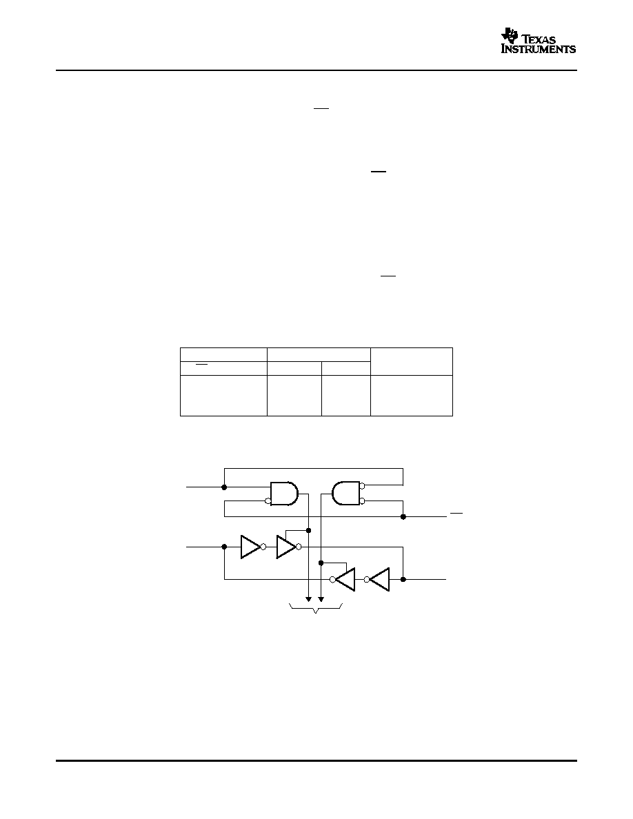
DIR
OE
A1
B1
To Seven Other Channels
2
3
22
21
SN74LVCH8T245
8-BIT DUAL-SUPPLY BUS TRANSCEIVER
WITH CONFIGURABLE VOLTAGE TRANSLATION AND 3-STATE OUTPUTS
SCES637 ≠ AUGUST 2005
The SN74LVCH8T245 is designed for asynchronous communication between two data buses. The logic levels of
the direction-control (DIR) input and the output-enable (OE) input activate either the B-port outputs or the A-port
outputs or place both output ports into the high-impedance mode. The device transmits data from the A bus to
the B bus when the B-port outputs are activated, and from the B bus to the A bus when the A-port outputs are
activated. The input circuitry on both A and B ports is always active and must have a logic HIGH or LOW level
applied to prevent excess I
CC
and I
CCZ
.
The SN74LVCH8T245 is designed so that the control pins (DIR and OE) are supplied by V
CCA
.
Active bus-hold circuitry holds unused or undriven inputs at a valid logic state. Use of pullup or pulldown resistors
with the bus-hold circuitry is not recommended.
This device is fully specified for partial-power-down applications using I
off
. The I
off
circuitry disables the outputs,
preventing damaging current backflow through the device when it is powered down.
The V
CC
isolation feature ensures that if either V
CC
input is at GND, then both ports are in the high-impedance
state.
To ensure the high-impedance state during power up or power down, OE should be tied to V
CC
through a pullup
resistor; the minimum value of the resistor is determined by the current-sinking capability of the driver.
FUNCTION TABLE
(1)
(EACH 8-BIT SECTION)
CONTROL INPUTS
OUTPUT CIRCUITS
OPERATION
OE
DIR
A PORT
B PORT
L
L
Enabled
Hi-Z
B data to A bus
L
H
Hi-Z
Enabled
A data to B bus
H
X
Hi-Z
Hi-Z
Isolation
(1)
Input circuits of the data I/Os are always active.
LOGIC DIAGRAM (POSITIVE LOGIC)
2
www.ti.com
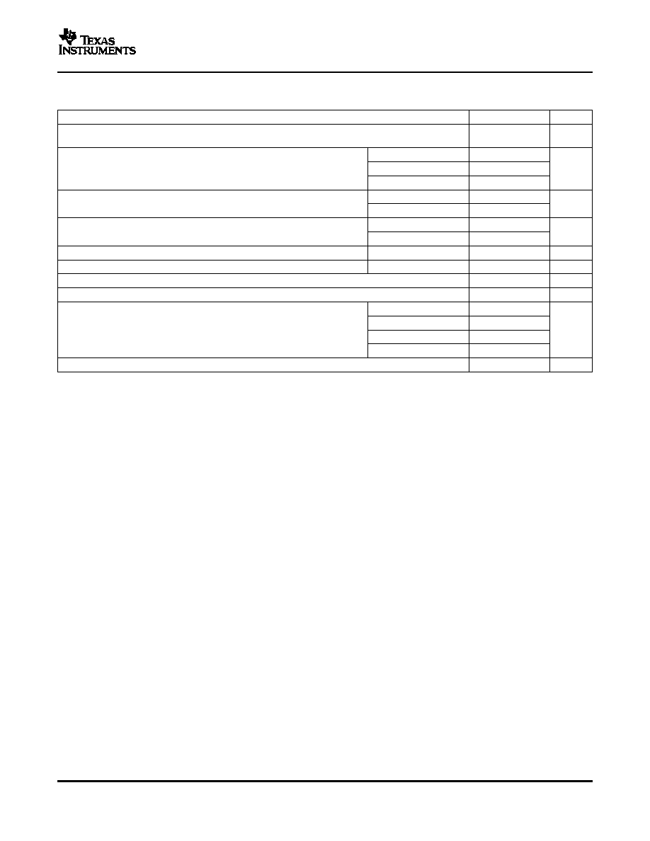
Absolute Maximum Ratings
(1)
SN74LVCH8T245
8-BIT DUAL-SUPPLY BUS TRANSCEIVER
WITH CONFIGURABLE VOLTAGE TRANSLATION AND 3-STATE OUTPUTS
SCES637 ≠ AUGUST 2005
over operating free-air temperature range (unless otherwise noted)
MIN
MAX
UNIT
V
CCA
Supply voltage range
≠0.5
6.5
V
V
CCB
I/O ports (A port)
≠0.5
6.5
V
I
Input voltage range
(2)
I/O ports (B port)
≠0.5
6.5
V
Control inputs
≠0.5
6.5
A port
≠0.5
6.5
Voltage range applied to any output
V
O
V
in the high-impedance or power-off state
(2)
B port
≠0.5
6.5
A port
≠0.5 V
CCA
+ 0.5
V
O
Voltage range applied to any output in the high or low state
(2) (3)
V
B port
≠0.5 V
CCB
+ 0.5
I
IK
Input clamp current
V
I
< 0
≠50
mA
I
OK
Output clamp current
V
O
< 0
≠50
mA
I
O
Continuous output current
±
50
mA
Continuous current through each V
CCA
, V
CCB
, and GND
±
100
mA
DB package
70
DGV package
58
JA
Package thermal impedance
(4)
∞
C/W
PW package
88
RHL package
43
T
stg
Storage temperature range
≠65
150
∞
C
(1)
Stresses beyond those listed under "absolute maximum ratings" may cause permanent damage to the device. These are stress ratings
only, and functional operation of the device at these or any other conditions beyond those indicated under "recommended operating
conditions" is not implied. Exposure to absolute-maximum-rated conditions for extended periods may affect device reliability.
(2)
The input and output negative-voltage ratings may be exceeded if the input and output current ratings are observed.
(3)
The output positive-voltage rating may be exceeded up to 6.5 V maximum if the output current rating is observed.
(4)
The package thermal impedance is calculated in accordance with JESD 51-7.
3
www.ti.com
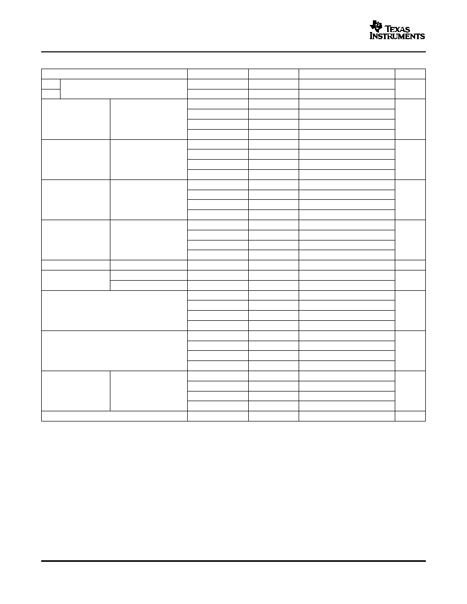
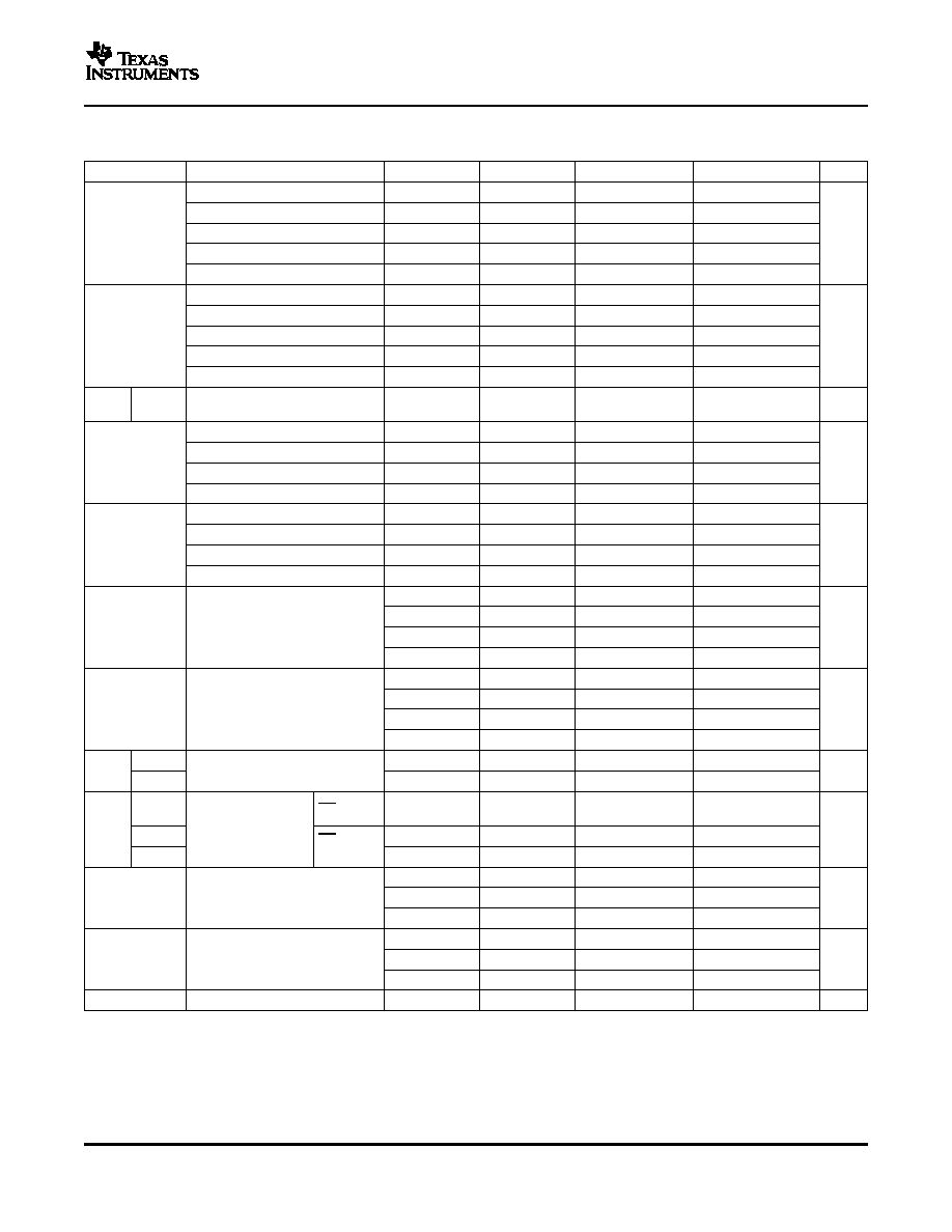
Recommended Operating Conditions
(1) (2) (3)
SN74LVCH8T245
8-BIT DUAL-SUPPLY BUS TRANSCEIVER
WITH CONFIGURABLE VOLTAGE TRANSLATION AND 3-STATE OUTPUTS
SCES637 ≠ AUGUST 2005
V
CCI
V
CCO
MIN
MAX
UNIT
V
CCA
1.65
5.5
Supply voltage
V
V
CCB
1.65
5.5
1.65 V to 1.95 V
V
CCI
◊
0.65
2.3 V to 2.7 V
1.7
High-level
V
IH
Data inputs
(4)
V
input voltage
3 V to 3.6 V
2
4.5 V to 5.5 V
V
CCI
◊
0.7
1.65 V to 1.95 V
V
CCI
◊
0.35
2.3 V to 2.7 V
0.7
Low-level
V
IL
Data inputs
(4)
V
input voltage
3 V to 3.6 V
0.8
4.5 V to 5.5 V
V
CCI
◊
0.3
1.65 V to 1.95 V
V
CCA
◊
0.65
2.3 V to 2.7 V
1.7
High-level
Control inputs
V
IH
V
input voltage
(referenced to V
CCA
)
(5)
3 V to 3.6 V
2
4.5 V to 5.5 V
V
CCA
◊
0.7
1.65 V to 1.95 V
V
CCA
◊
0.35
2.3 V to 2.7 V
0.7
Low-level
Control inputs
V
IL
V
input voltage
(referenced to V
CCA
)
(5)
3 V to 3.6 V
0.8
4.5 V to 5.5 V
V
CCA
◊
0.3
V
I
Input voltage
Control inputs
0
5.5
V
Active state
0
V
CCO
Input/output
V
I/O
V
voltage
3-State
0
5.5
1.65 V to 1.95 V
≠4
2.3 V to 2.7 V
≠8
I
OH
High-level output current
mA
3 V to 3.6 V
≠24
4.5 V to 5.5 V
≠32
1.65 V to 1.95 V
4
2.3 V to 2.7 V
8
I
OL
Low-level output current
mA
3 V to 3.6 V
24
4.5 V to 5.5 V
32
1.65 V to 1.95 V
20
2.3 V to 2.7 V
20
Input transition
t/
v
Data inputs
ns/V
rise or fall rate
3 V to 3.6 V
10
4.5 V to 5.5 V
5
T
A
Operating free-air temperature
≠40
85
∞
C
(1)
V
CCI
is the V
CC
associated with the data input port.
(2)
V
CCO
is the V
CC
associated with the output port.
(3)
All unused control inputs of the device must be held at V
CCA
or GND to ensure proper device operation and minimize power
consumption. Refer to the TI application report, Implications of Slow or Floating CMOS Inputs, literature number SCBA004.
(4)
For V
CCI
values not specified in the data sheet, V
IH
min = V
CCI
◊
0.7 V, V
IL
max = V
CCI
◊
0.3 V.
(5)
For V
CCA
values not specified in the data sheet, V
IH
min = V
CCA
◊
0.7 V, V
IL
max = V
CCA
◊
0.3 V.
4
www.ti.com
Electrical Characteristics
(1) (2)
SN74LVCH8T245
8-BIT DUAL-SUPPLY BUS TRANSCEIVER
WITH CONFIGURABLE VOLTAGE TRANSLATION AND 3-STATE OUTPUTS
SCES637 ≠ AUGUST 2005
over recommended operating free-air temperature range (unless otherwise noted)
PARAMETER
TEST CONDITIONS
V
CCA
V
CCB
MIN
TYP
MAX
MIN
MAX
UNIT
I
OH
= ≠100
µ
A,
V
I
= V
IH
1.65 V to 4.5 V
1.65 V to 4.5 V
V
CCO
≠ 0.1
I
OH
= ≠4 mA,
V
I
= V
IH
1.65 V
1.65 V
1.2
V
OH
I
OH
= ≠8 mA,
V
I
= V
IH
2.3 V
2.3 V
1.9
V
I
OH
= ≠24 mA,
V
I
= V
IH
3 V
3 V
2.4
I
OH
= ≠32 mA,
V
I
= V
IH
4.5 V
4.5 V
3.8
I
OL
= 100
µ
A,
V
I
= V
IL
1.65 V to 4.5 V
1.65 V to 4.5 V
0.1
I
OL
= 4 mA,
V
I
= V
IL
1.65 V
1.65 V
0.45
V
OL
I
OL
= 8 mA,
V
I
= V
IL
2.3 V
2.3 V
0.3
V
I
OL
= 24 mA,
V
I
= V
IL
3 V
3 V
0.55
I
OL
= 32 mA,
V
I
= V
IL
4.5 V
4.5 V
0.55
Control
I
I
V
I
= V
CCA
or GND
1.65 V to 5.5 V
1.65 V to 5.5 V
±
0.5
±
1
±
2
µ
A
inputs
V
I
= 0.58 V
1.65 V
1.65 V
15
V
I
= 0.7 V
2.3 V
2.3 V
45
I
BHL
(3)
µ
A
V
I
= 0.8 V
3 V
3 V
75
V
I
= 0.1.35 V
4.5 V
4.5 V
100
V
I
= 1.07 V
1.65 V
1.65 V
≠15
V
I
= 1.7 V
2.3 V
2.3 V
≠45
I
BHH
(4)
µ
A
V
I
= 2 V
3 V
3 V
≠75
V
I
= 3.15 V
4.5 V
4.5 V
≠100
1.95 V
1.95 V
200
2.7 V
2.7 V
300
I
BHLO
(5)
V
I
= 0 to V
CC
µ
A
3.6 V
3.6 V
500
5.5 V
5.5 V
900
1.95 V
1.95 V
≠200
2.7 V
2.7 V
≠300
I
BHHO
(6)
V
I
= 0 to V
CC
µ
A
3.6 V
3.6 V
≠500
5.5 V
5.5 V
≠900
A port
0 V
0 to 5.5 V
±
0.5
±
1
±
2
I
off
V
I
or V
O
= 0 to 5.5 V
µ
A
B port
0 to 5.5 V
0 V
±
0.5
±
1
±
2
A or B
OE = V
IH
1.65 V to 5.5 V
1.65 V to 5.5 V
±
1
±
2
port
V
O
= V
CCO
or GND,
I
OZ
µ
A
B port
V
I
= V
CCI
or GND
0 V
5.5 V
±
1
±
2
OE = don't
care
A port
5.5 V
0 V
±
1
±
2
1.65 V to 5.5 V
1.65 V to 5.5 V
20
I
CCA
V
I
= V
CCI
or GND,
I
O
= 0
5 V
0 V
20
µ
A
0 V
5 V
≠2
1.65 V to 5.5 V
1.65 V to 5.5 V
20
I
CCB
V
I
= V
CCI
or GND,
I
O
= 0
5 V
0 V
≠2
µ
A
0 V
5 V
20
I
CCA
+ I
CCB
V
I
= V
CCI
or GND,
I
O
= 0
1.65 V to 5.5 V
1.65 V to 5.5 V
30
µ
A
(1)
V
CCO
is the V
CC
associated with the output port.
(2)
V
CCI
is the V
CC
associated with the input port.
(3)
The bus-hold circuit can sink at least the minimum low sustaining current at V
IL
max. I
BHL
should be measured after lowering V
IN
to GND
and then raising it to V
IL
max.
(4)
The bus-hold circuit can source at least the minimum high sustaining current at V
IH
min. I
BHH
should be measured after raising V
IN
to
V
CC
and then lowering it to V
IH
min.
(5)
An external driver must source at least I
BHLO
to switch this node from low to high.
(6)
An external driver must sink at least I
BHHO
to switch this node from high to low.
5