SN74LVCHR16245A (Rev. O)
SN74LVCHR16245A
16 BIT BUS TRANSCEIVER
WITH 3 STATE OUTPUTS
SCAS582O - NOVEMBER 1996 - REVISED SEPTEMBER 2003
1
POST OFFICE BOX 655303
·
DALLAS, TEXAS 75265
D
Member of the Texas Instruments
Widebus
Family
D
Operates From 1.65 V to 3.6 V
D
Inputs Accept Voltages to 5.5 V
D
Max t
pd
of 4.8 ns at 3.3 V
D
Typical V
OLP
(Output Ground Bounce)
<0.8 V at V
CC
= 3.3 V, T
A
= 25
°
C
D
Typical V
OHV
(Output V
OH
Undershoot)
>2 V at V
CC
= 3.3 V, T
A
= 25
°
C
D
Supports Mixed-Mode Signal Operation on
All Ports (5-V Input/Output Voltage With
3.3-V V
CC
)
D
Bus Hold on Data Inputs Eliminates the
Need for External Pullup/Pulldown
Resistors
D
All Outputs Have Equivalent 26-
Series
Resistors, So No External Resistors Are
Required
D
I
off
Supports Partial-Power-Down Mode
Operation
D
Latch-Up Performance Exceeds 250 mA Per
JESD 17
D
ESD Protection Exceeds JESD 22
- 2000-V Human-Body Model (A114-A)
- 200-V Machine Model (A115-A)
description/ordering information
This 16-bit (dual-octal) noninverting bus transceiver is designed for 1.65-V to 3.6-V V
CC
operation.
The SN74LVCHR16245A is designed for asynchronous communication between data buses. The
control-function implementation minimizes external-timing requirements.
This device can be used as two 8-bit transceivers or one 16-bit transceiver. It allows data transmission from the
A bus to the B bus or from the B bus to the A bus, depending on the logic level at the direction-control (DIR)
input. The output-enable (OE) input can disable the device so that the buses effectively are isolated.
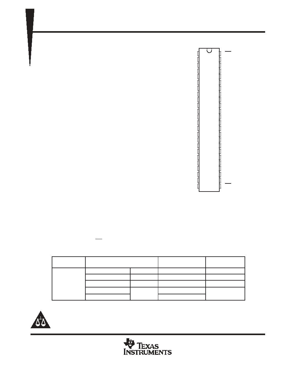
ORDERING INFORMATION
TA
PACKAGE
ORDERABLE
PART NUMBER
TOP-SIDE
MARKING
SSOP - DL
Tape and reel
SN74LVCHR16245ALR
LVCHR16245A
TSSOP - DGG
Tape and reel
SN74LVCHR16245AGR
LVCHR16245A
-40
°
C to 85
°
C
TVSOP - DGV
Tape and reel
SN74LVCHR16245AVR
LDR245A
-40 C to 85 C
VFBGA - GQL
Tape and reel
SN74LVCHR16245AKR
LR245A
VFBGA - ZQL (Pb-free)
Tape and reel
74LVCHR16245AZQLR
LR245A
Package drawings, standard packing quantities, thermal data, symbolization, and PCB design guidelines are
available at www.ti.com/sc/package.
PRODUCTION DATA information is current as of publication date.
Products conform to specifications per the terms of Texas Instruments
standard warranty. Production processing does not necessarily include
testing of all parameters.
Copyright
2003, Texas Instruments Incorporated
Please be aware that an important notice concerning availability, standard warranty, and use in critical applications of
Texas Instruments semiconductor products and disclaimers thereto appears at the end of this data sheet.
Widebus is a trademark of Texas Instruments.
DGG, DGV, OR DL PACKAGE
(TOP VIEW)
1
2
3
4
5
6
7
8
9
10
11
12
13
14
15
16
17
18
19
20
21
22
23
24
48
47
46
45
44
43
42
41
40
39
38
37
36
35
34
33
32
31
30
29
28
27
26
25
1DIR
1B1
1B2
GND
1B3
1B4
V
CC
1B5
1B6
GND
1B7
1B8
2B1
2B2
GND
2B3
2B4
V
CC
2B5
2B6
GND
2B7
2B8
2DIR
1OE
1A1
1A2
GND
1A3
1A4
V
CC
1A5
1A6
GND
1A7
1A8
2A1
2A2
GND
2A3
2A4
V
CC
2A5
2A6
GND
2A7
2A8
2OE
SN74LVCHR16245A
16 BIT BUS TRANSCEIVER
WITH 3 STATE OUTPUTS
SCAS582O - NOVEMBER 1996 - REVISED SEPTEMBER 2003
2
POST OFFICE BOX 655303
·
DALLAS, TEXAS 75265
description/ordering information (continued)
All outputs, which are designed to sink up to 12 mA, include equivalent 26-
W
series resistors to reduce
overshoot and undershoot.
Inputs can be driven from either 3.3-V or 5-V devices. This feature allows the use of this device as a translator
in a mixed 3.3-V/5-V system environment.
To ensure the high-impedance state during power up or power down, OE should be tied to V
CC
through a pullup
resistor; the minimum value of the resistor is determined by the current-sinking capability of the driver.
This device is fully specified for partial-power-down applications using I
off
. The I
off
circuitry disables the outputs,
preventing damaging current backflow through the device when it is powered down.
Active bus-hold circuitry is provided to hold unused or floating data inputs at a valid logic level. Use of pullup
or pulldown resistors with the bus-hold circuitry is not recommended. The bus-hold circuitry is part of the input
circuit and is not disabled by OE or DIR.
terminal assignments
1
2
3
4
5
6
A
1DIR
NC
NC
NC
NC
1OE
B
1B2
1B1
GND
GND
1A1
1A2
C
1B4
1B3
VCC
VCC
1A3
1A4
D
1B6
1B5
GND
GND
1A5
1A6
E
1B8
1B7
1A7
1A8
F
2B1
2B2
2A2
2A1
G
2B3
2B4
GND
GND
2A4
2A3
H
2B5
2B6
VCC
VCC
2A6
2A5
J
2B7
2B8
GND
GND
2A8
2A7
K
2DIR
NC
NC
NC
NC
2OE
NC - No internal connection
FUNCTION TABLE
(each 8-bit section)
INPUTS
OPERATION
OE
DIR
OPERATION
L
L
B data to A bus
L
H
A data to B bus
H
X
Isolation
GQL OR ZQL PACKAGE
(TOP VIEW)
J
H
G
F
E
D
C
B
A
2
1
3
4
6
5
K
SN74LVCHR16245A
16 BIT BUS TRANSCEIVER
WITH 3 STATE OUTPUTS
SCAS582O - NOVEMBER 1996 - REVISED SEPTEMBER 2003
3
POST OFFICE BOX 655303
·
DALLAS, TEXAS 75265
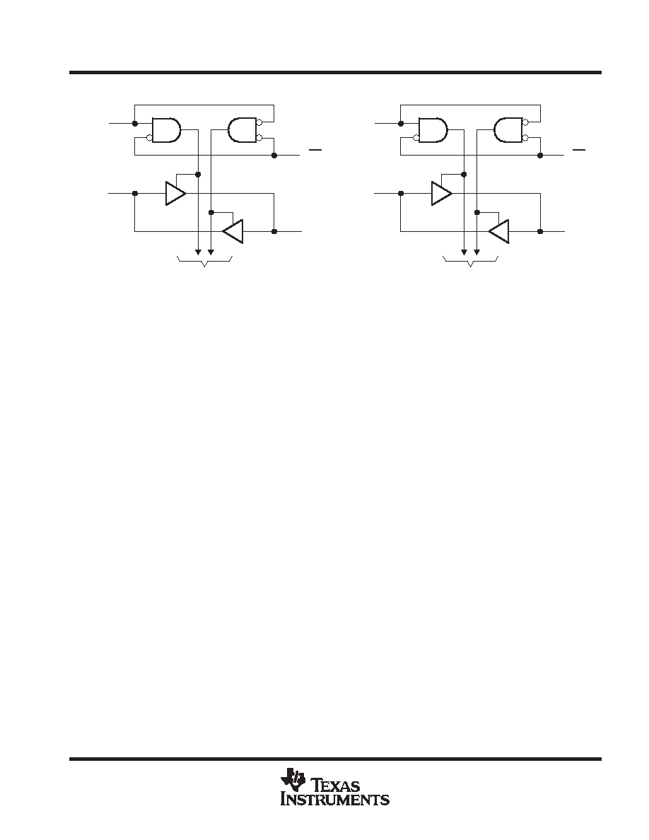
logic diagram (positive logic)
To Seven Other Channels
1DIR
1A1
1B1
1OE
To Seven Other Channels
2DIR
2A1
2B1
2OE
1
47
24
36
48
2
25
13
Pin numbers shown are for the DGG, DGV, and DL packages.
absolute maximum ratings over operating free-air temperature range (unless otherwise noted)
Supply voltage range, V
CC
-0.5 V to 6.5 V
. . . . . . . . . . . . . . . . . . . . . . . . . . . . . . . . . . . . . . . . . . . . . . . . . . . . . . . . .
Input voltage range, V
I
(see Note 1)
-0.5 V to 6.5 V
. . . . . . . . . . . . . . . . . . . . . . . . . . . . . . . . . . . . . . . . . . . . . . . . .
Voltage range applied to any output in the high-impedance or power-off state, V
O
(see Note 1)
-0.5 V to 6.5 V
. . . . . . . . . . . . . . . . . . . . . . . . . . . . . . . . . . . . . . . . . . . . . . . . . . . . . . . . . . . . . . . . . . .
Voltage range applied to any output in the high or low state, V
O
(see Notes 1 and 2)
-0.5 V to V
CC
+ 0.5 V
. . . . . . . . . . . . . . . . . . . . . . . . . . . . . . . . . . . . . . . . . . . . . . . . . . . . . . .
Input clamp current, I
IK
(V
I
< 0)
-50 mA
. . . . . . . . . . . . . . . . . . . . . . . . . . . . . . . . . . . . . . . . . . . . . . . . . . . . . . . . . . .
Output clamp current, I
OK
(V
O
< 0)
-50 mA
. . . . . . . . . . . . . . . . . . . . . . . . . . . . . . . . . . . . . . . . . . . . . . . . . . . . . . . .
Continuous output current, I
O
±
50 mA
. . . . . . . . . . . . . . . . . . . . . . . . . . . . . . . . . . . . . . . . . . . . . . . . . . . . . . . . . . . . .
Continuous current through each V
CC
or GND
±
100 mA
. . . . . . . . . . . . . . . . . . . . . . . . . . . . . . . . . . . . . . . . . . . . .
Package thermal impedance,
JA
(see Note 3): DGG package
70
°
C/W
. . . . . . . . . . . . . . . . . . . . . . . . . . . . . . .
DGV package
58
°
C/W
. . . . . . . . . . . . . . . . . . . . . . . . . . . . . . . .
DL package
63
°
C/W
. . . . . . . . . . . . . . . . . . . . . . . . . . . . . . . . .
GQL/ZQL package
42
°
C/W
. . . . . . . . . . . . . . . . . . . . . . . . . . .
Storage temperature range, T
stg
-65
°
C to 150
°
C
. . . . . . . . . . . . . . . . . . . . . . . . . . . . . . . . . . . . . . . . . . . . . . . . . . .
Stresses beyond those listed under "absolute maximum ratings" may cause permanent damage to the device. These are stress ratings only, and
functional operation of the device at these or any other conditions beyond those indicated under "recommended operating conditions" is not
implied. Exposure to absolute-maximum-rated conditions for extended periods may affect device reliability.
NOTES:
1. The input negative-voltage and output voltage ratings may be exceeded if the input and output current ratings are observed.
2. The value of VCC is provided in the recommended operating conditions table.
3. The package thermal impedance is calculated in accordance with JESD 51-7.
SN74LVCHR16245A
16 BIT BUS TRANSCEIVER
WITH 3 STATE OUTPUTS
SCAS582O - NOVEMBER 1996 - REVISED SEPTEMBER 2003
4
POST OFFICE BOX 655303
·
DALLAS, TEXAS 75265
recommended operating conditions (see Note 4)
MIN
MAX
UNIT
VCC
Supply voltage
Operating
1.65
3.6
V
VCC
Supply voltage
Data retention only
1.5
V
VCC = 1.65 V to 1.95 V
0.65
×
VCC
VIH
High-level input voltage
VCC = 2.3 V to 2.7 V
1.7
V
VIH
High-level input voltage
VCC = 2.7 V to 3.6 V
2
V
VCC = 1.65 V to 1.95 V
0.35
×
VCC
VIL
Low-level input voltage
VCC = 2.3 V to 2.7 V
0.7
V
VIL
Low-level input voltage
VCC = 2.7 V to 3.6 V
0.8
V
VI
Input voltage
0
5.5
V
VO
Output voltage
High or low state
0
VCC
V
VO
Output voltage
3-state
0
5.5
V
VCC = 1.65 V
-2
IOH
High-level output current
VCC = 2.3 V
-4
mA
IOH
High-level output current
VCC = 2.7 V
-8
mA
VCC = 3 V
-12
VCC = 1.65 V
2
IOL
Low-level output current
VCC = 2.3 V
4
mA
IOL
Low-level output current
VCC = 2.7 V
8
mA
VCC = 3 V
12
t/
v
Input transition rise or fall rate
10
ns/V
TA
Operating free-air temperature
-40
85
°
C
NOTE 4: All unused control inputs of the device must be held at VCC or GND to ensure proper device operation. Refer to the TI application report,
Implications of Slow or Floating CMOS Inputs, literature number SCBA004.
SN74LVCHR16245A
16 BIT BUS TRANSCEIVER
WITH 3 STATE OUTPUTS
SCAS582O - NOVEMBER 1996 - REVISED SEPTEMBER 2003
5
POST OFFICE BOX 655303
·
DALLAS, TEXAS 75265
electrical characteristics over recommended operating free-air temperature range (unless
otherwise noted)
PARAMETER
TEST CONDITIONS
VCC
MIN
TYP
MAX
UNIT
IOH = -100
µ
A
1.65 V to 3.6 V
VCC-0.2
IOH = -2 mA
1.65 V
1.2
IOH = -4 mA
2.3 V
1.7
VOH
IOH = -4 mA
2.7 V
2.2
V
VOH
IOH = -6 mA
3 V
2.4
V
IOH = -8 mA
2.7 V
2
IOH = -12 mA
3 V
2
IOL = 100
µ
A
1.65 V to 3.6 V
0.2
IOL = 2 mA
1.65 V
0.45
IOL = 4 mA
2.3 V
0.7
VOL
IOL = 4 mA
2.7 V
0.4
V
VOL
IOL = 6 mA
3 V
0.55
V
IOL = 8 mA
2.7 V
0.6
IOL = 12 mA
3 V
0.8
II
Control inputs
VI = 0 to 5.5 V
3.6 V
±
5
µ
A
VI = 0.58 V
1.65 V
VI = 1.07 V
1.65 V
VI = 0.7 V
2.3 V
45
II(hold)
A or B ports
VI = 1.7 V
2.3 V
-45
µ
A
II(hold)
A or B ports
VI = 0.8 V
3 V
75
µ
A
VI = 2 V
3 V
-75
VI = 0 to 3.6 V§
3.6 V
±
500
Ioff
VI or VO = 5.5 V
0
±
10
µ
A
IOZ¶
VO = 0 V or (VCC to 5.5 V)
2.3 V to 3.6 V
±
5
µ
A
ICC
VI = VCC or GND
IO = 0
3.6 V
20
A
ICC
3.6 V
VI
5.5 V#
IO = 0
3.6 V
20
µ
A
ICC
One input at VCC - 0.6 V,
Other inputs at VCC or GND
2.7 V to 3.6 V
500
µ
A
Ci
Control inputs
VI = VCC or GND
3.3 V
3
pF
Cio
A or B ports
VO = VCC or GND
3.3 V
12
pF
All typical values are at VCC = 3.3 V, TA = 25
°
C.
This information was not available at the time of publication.
§ This is the bus-hold maximum dynamic current. It is the minimum overdrive current required to switch the input from one state to another.
¶ For the total leakage current in an I/O port, please consult the II(hold) specification for the input voltage condition 0 V
<
VI
<
VCC, and the IOZ
specification for the input voltage conditions VI = 0 V or VI = VCC to 5.5 V. The bus-hold current, at input voltages greater than VCC, is negligible.
# This applies in the disabled state only.
switching characteristics over recommended operating free-air temperature range (unless
otherwise noted) (see Figure 1)
PARAMETER
FROM
(INPUT)
TO
(OUTPUT)
VCC = 1.8 V
±
0.15 V
VCC = 2.5 V
±
0.2 V
VCC = 2.7 V
VCC = 3.3 V
±
0.3 V
UNIT
PARAMETER
(INPUT)
(OUTPUT)
MIN
MAX
MIN
MAX
MIN
MAX
MIN
MAX
UNIT
tpd
A or B
B or A
1
12.5
1
9.5
1
5.7
1.5
4.8
ns
ten
OE
A or B
1
15.8
1
12.2
1
7.9
1.5
6.3
ns
tdis
OE
A or B
1
19.2
1
11.9
1
8.3
2.2
7.4
ns