SN54LVT16245B, SN74LVT16245B
3.3 V ABT 16 BIT BUS TRANSCEIVERS
WITH 3 STATE OUTPUTS
SCBS715C - FEBRUARY 2000 - REVISED SEPTEMBER 2003
1
POST OFFICE BOX 655303
∑
DALLAS, TEXAS 75265
POST OFFICE BOX 1443
∑
HOUSTON, TEXAS 77251-1443
D
Members of the Texas Instruments
Widebus
Family
D
State-of-the-Art Advanced BiCMOS
Technology (ABT) Design for 3.3-V
Operation and Low Static-Power
Dissipation
D
Support Mixed-Mode Signal Operation
(5-V Input and Output Voltages With
3.3-V V
CC
)
D
Support Unregulated Battery Operation
Down to 2.7 V
D
Typical V
OLP
(Output Ground Bounce)
<0.8 V at V
CC
= 3.3 V, T
A
= 25
∞
C
D
I
off
and Power-Up 3-State Support Hot
Insertion
D
Distributed V
CC
and GND Pins Minimize
High-Speed Switching Noise
D
Flow-Through Architecture Optimizes PCB
Layout
D
Latch-Up Performance Exceeds 100 mA Per
JESD 78, Class II
D
ESD Protection Exceeds JESD 22
- 2000-V Human-Body Model (A114-A)
- 200-V Machine Model (A115-A)
- 1000-V Charged-Device Model (C101)
description/ordering information
The 'LVT16245B devices are 16-bit (dual-octal) noninverting 3-state transceivers designed for low-voltage
(3.3-V) V
CC
operation, but with the capability to provide a TTL interface to a 5-V system environment.
ORDERING INFORMATION
TA
PACKAGE
ORDERABLE
PART NUMBER
TOP-SIDE
MARKING
SSOP - DL
Tube
SN74LVT16245BDL
LVT16245B
SSOP - DL
Tape and reel
SN74LVT16245BDLR
LVT16245B
-40
∞
C to 85
∞
C
TSSOP - DGG
Tape and reel
SN74LVT16245BDGGR
LVT16245B
-40
∞
C to 85
∞
C
TVSOP - DGV
Tape and reel
SN74LVT16245BDGVR
VD245B
VFBGA - GQL
Tape and reel
SN74LVT16245BGQLR
VD245B
VFBGA - ZQL (Pb-free)
Tape and reel
SN74LVT16245BZQLR
VD245B
-55
∞
C to 125
∞
C
CFP - WD
Tube
SNJ54LVT16245BWD
SNJ54LVT16245BWD
Package drawings, standard packing quantities, thermal data, symbolization, and PCB design guidelines are available at
www.ti.com/sc/package.
Copyright
2003, Texas Instruments Incorporated
UNLESS OTHERWISE NOTED this document contains PRODUCTION
DATA information current as of publication date. Products conform to
specifications per the terms of Texas Instruments standard warranty.
Production processing does not necessarily include testing of all
parameters.
Widebus is a trademark of Texas Instruments.
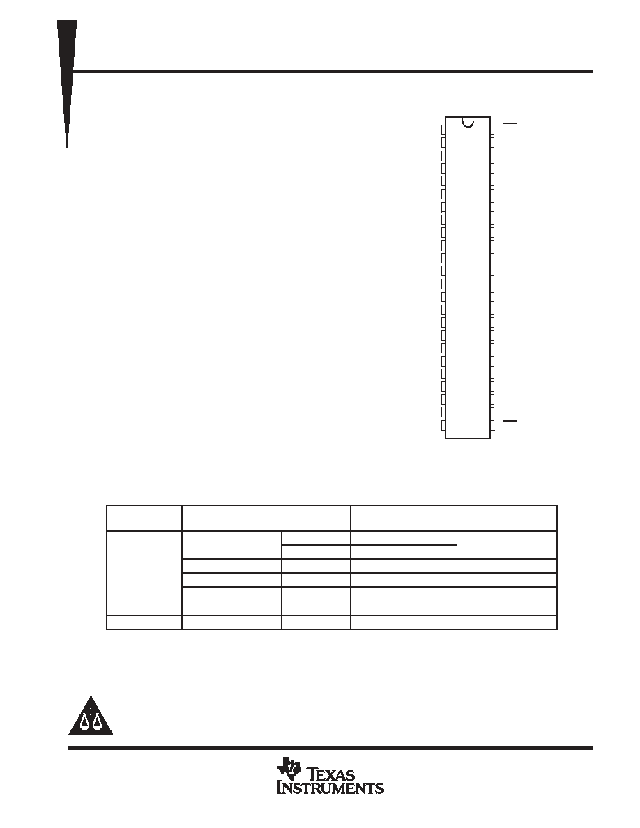
SN54LVT16245B . . . WD PACKAGE
SN74LVT16245B . . . DGG, DGV, OR DL PACKAGE
(TOP VIEW)
1
2
3
4
5
6
7
8
9
10
11
12
13
14
15
16
17
18
19
20
21
22
23
24
48
47
46
45
44
43
42
41
40
39
38
37
36
35
34
33
32
31
30
29
28
27
26
25
1DIR
1B1
1B2
GND
1B3
1B4
V
CC
1B5
1B6
GND
1B7
1B8
2B1
2B2
GND
2B3
2B4
V
CC
2B5
2B6
GND
2B7
2B8
2DIR
1OE
1A1
1A2
GND
1A3
1A4
V
CC
1A5
1A6
GND
1A7
1A8
2A1
2A2
GND
2A3
2A4
V
CC
2A5
2A6
GND
2A7
2A8
2OE
Please be aware that an important notice concerning availability, standard warranty, and use in critical applications of
Texas Instruments semiconductor products and disclaimers thereto appears at the end of this data sheet.
SN54LVT16245B, SN74LVT16245B
3.3 V ABT 16 BIT BUS TRANSCEIVERS
WITH 3 STATE OUTPUTS
SCBS715C - FEBRUARY 2000 - REVISED SEPTEMBER 2003
2
POST OFFICE BOX 655303
∑
DALLAS, TEXAS 75265
POST OFFICE BOX 1443
∑
HOUSTON, TEXAS 77251-1443
description/ordering information (continued)
These devices can be used as two 8-bit transceivers or one 16-bit transceiver. They allow data transmission
from the A bus to the B bus or from the B bus to the A bus, depending on the logic level at the direction-control
(DIR) input. The output-enable (OE) input can be used to disable the devices so that the buses are
effectively isolated.
When V
CC
is between 0 and 1.5 V, the devices are in the high-impedance state during power up or power down.
However, to ensure the high-impedance state above 1.5 V, OE should be tied to V
CC
through a pullup resistor;
the minimum value of the resistor is determined by the current-sinking capability of the driver.
These devices are fully specified for hot-insertion applications using I
off
and power-up 3-state. The I
off
circuitry
disables the outputs, preventing damaging current backflow through the devices when they are powered down.
The power-up 3-state circuitry places the outputs in the high-impedance state during power up and power down,
which prevents driver conflict.
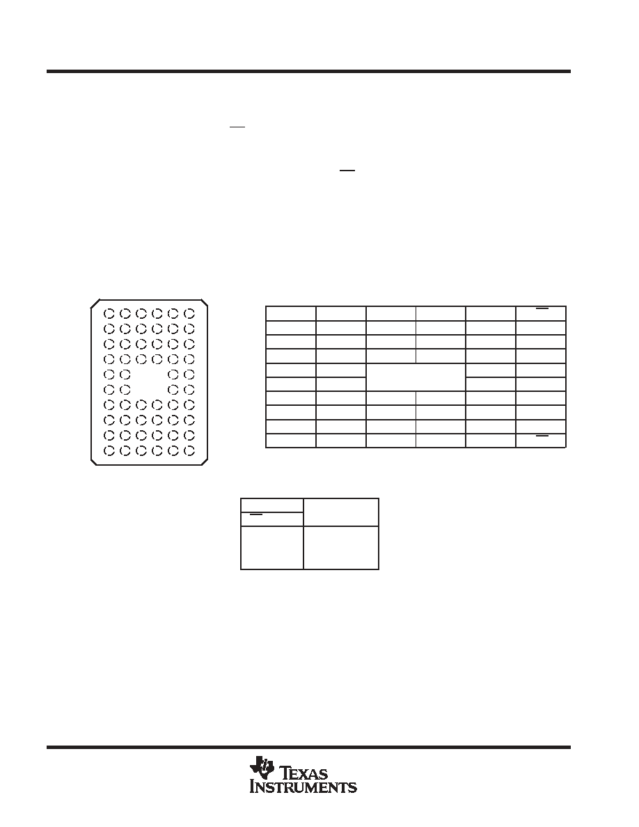
terminal assignments
1
2
3
4
5
6
A
1DIR
NC
NC
NC
NC
1OE
B
1B2
1B1
GND
GND
1A1
1A2
C
1B4
1B3
VCC
VCC
1A3
1A4
D
1B6
1B5
GND
GND
1A5
1A6
E
1B8
1B7
1A7
1A8
F
2B1
2B2
2A2
2A1
G
2B3
2B4
GND
GND
2A4
2A3
H
2B5
2B6
VCC
VCC
2A6
2A5
J
2B7
2B8
GND
GND
2A8
2A7
K
2DIR
NC
NC
NC
NC
2OE
NC - No internal connection
FUNCTION TABLE
(each 8-bit section)
INPUTS
OPERATION
OE
DIR
OPERATION
L
L
B data to A bus
L
H
A data to B bus
H
X
Isolation
GQL OR ZQL PACKAGE
(TOP VIEW)
A
B
C
D
E
F
G
H
J
K
1
2
3
4
5
6
SN54LVT16245B, SN74LVT16245B
3.3 V ABT 16 BIT BUS TRANSCEIVERS
WITH 3 STATE OUTPUTS
SCBS715C - FEBRUARY 2000 - REVISED SEPTEMBER 2003
3
POST OFFICE BOX 655303
∑
DALLAS, TEXAS 75265
POST OFFICE BOX 1443
∑
HOUSTON, TEXAS 77251-1443
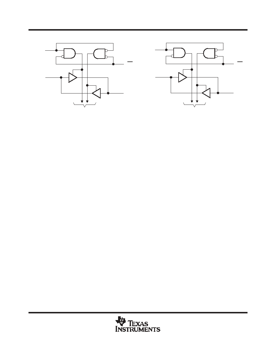
logic diagram (positive logic)
To Seven Other Channels
1DIR
1A1
1B1
1OE
To Seven Other Channels
2DIR
2A1
2B1
2OE
1
47
24
36
48
2
25
13
Pin numbers shown are for the DGG, DGV, DL, and WD packages.
absolute maximum ratings over operating free-air temperature range (unless otherwise noted)
Supply voltage range, V
CC
-0.5 V to 4.6 V
. . . . . . . . . . . . . . . . . . . . . . . . . . . . . . . . . . . . . . . . . . . . . . . . . . . . . . . . .
Input voltage range, V
I
(see Note 1)
-0.5 V to 7 V
. . . . . . . . . . . . . . . . . . . . . . . . . . . . . . . . . . . . . . . . . . . . . . . . . .
Voltage range applied to any output in the high-impedance
or power-off state, V
O
(see Note 1)
-0.5 V to 7 V
. . . . . . . . . . . . . . . . . . . . . . . . . . . . . . . . . . . . . . . . . . . . . . . .
Voltage range applied to any output in the high state, V
O
(see Note 1)
-0.5 V to V
CC
+ 0.5 V
. . . . . . . . . . . . .
Current into any output in the low state, I
O
: SN54LVT16245B 96
mA
. . . . . . . . . . . . . . . . . . . . . . . . . . . . . . . . .
SN74LVT16245B 128
mA
. . . . . . . . . . . . . . . . . . . . . . . . . . . . . . . .
Current into any output in the high state, I
O
(see Note 2): SN54LVT16245B
48 mA
. . . . . . . . . . . . . . . . . . . . .
SN74LVT16245B 64
mA
. . . . . . . . . . . . . . . . . . . . .
Input clamp current, I
IK
(V
I
< 0)
-50 mA
. . . . . . . . . . . . . . . . . . . . . . . . . . . . . . . . . . . . . . . . . . . . . . . . . . . . . . . . . . .
Output clamp current, I
OK
(V
O
< 0)
-50 mA
. . . . . . . . . . . . . . . . . . . . . . . . . . . . . . . . . . . . . . . . . . . . . . . . . . . . . . . .
Package thermal impedance,
JA
(see Note 3): DGG package
70
∞
C/W
. . . . . . . . . . . . . . . . . . . . . . . . . . . . . . .
DGV package
58
∞
C/W
. . . . . . . . . . . . . . . . . . . . . . . . . . . . . . . .
DL package
63
∞
C/W
. . . . . . . . . . . . . . . . . . . . . . . . . . . . . . . . .
GQL/ZQL package
42
∞
C/W
. . . . . . . . . . . . . . . . . . . . . . . . . . .
Storage temperature range, T
stg
-65
∞
C to 150
∞
C
. . . . . . . . . . . . . . . . . . . . . . . . . . . . . . . . . . . . . . . . . . . . . . . . . . .
Stresses beyond those listed under "absolute maximum ratings" may cause permanent damage to the device. These are stress ratings only, and
functional operation of the device at these or any other conditions beyond those indicated under "recommended operating conditions" is not
implied. Exposure to absolute-maximum-rated conditions for extended periods may affect device reliability.
NOTES:
1. The input and output negative-voltage ratings may be exceeded if the input and output clamp-current ratings are observed.
2. This current flows only when the output is in the high state and VO > VCC.
3. The package thermal impedance is calculated in accordance with JESD 51-7.
SN54LVT16245B, SN74LVT16245B
3.3 V ABT 16 BIT BUS TRANSCEIVERS
WITH 3 STATE OUTPUTS
SCBS715C - FEBRUARY 2000 - REVISED SEPTEMBER 2003
4
POST OFFICE BOX 655303
∑
DALLAS, TEXAS 75265
POST OFFICE BOX 1443
∑
HOUSTON, TEXAS 77251-1443
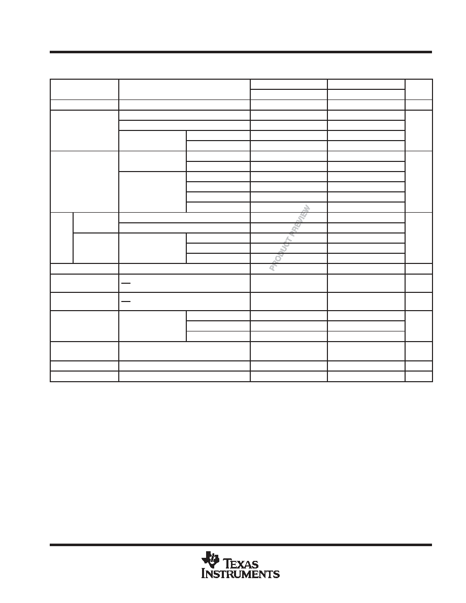
recommended operating conditions (see Note 4)
SN54LVT16245B
SN74LVT16245B
UNIT
MIN
MAX
MIN
MAX
UNIT
VCC
Supply voltage
2.7
3.6
2.7
3.6
V
VIH
High-level input voltage
2
2
V
VIL
Low-level input voltage
0.8
0.8
V
VI
Input voltage
5.5
5.5
V
IOH
High-level output current
-24
-32
mA
IOL
Low-level output current
48
64
mA
t/
v
Input transition rise or fall rate
Outputs enabled
10
10
ns/V
t/
VCC
Power-up ramp rate
200
200
µ
s/V
TA
Operating free-air temperature
-55
125
-40
85
∞
C
NOTE 4: All unused inputs of the device must at VCC or GND to ensure proper device operation. Refer to the TI application report, Implications
of Slow or Floating CMOS Inputs, literature number SCBA004.
PRODUCT PREVIEW information concerns products in the formative or
design phase of development. Characteristic data and other
specifications are design goals. Texas Instruments reserves the right to
change or discontinue these products without notice.
SN54LVT16245B, SN74LVT16245B
3.3 V ABT 16 BIT BUS TRANSCEIVERS
WITH 3 STATE OUTPUTS
SCBS715C - FEBRUARY 2000 - REVISED SEPTEMBER 2003
5
POST OFFICE BOX 655303
∑
DALLAS, TEXAS 75265
POST OFFICE BOX 1443
∑
HOUSTON, TEXAS 77251-1443
electrical characteristics over recommended operating free-air temperature range (unless
otherwise noted)
PARAMETER
TEST CONDITIONS
SN54LVT16245B
SN74LVT16245B
UNIT
PARAMETER
TEST CONDITIONS
MIN
TYP
MAX
MIN
TYP
MAX
UNIT
VIK
VCC = 2.7 V,
II = -18 mA
-1.2
-1.2
V
VCC = 2.7 V to 3.6 V,
IOH = -100
µ
A
VCC-0.2
VCC-0.2
VOH
VCC = 2.7 V,
IOH = -8 mA
2.4
2.4
V
VOH
VCC = 3 V
IOH = -24 mA
2
V
VCC = 3 V
IOH = -32 mA
2
VCC = 2.7 V
IOL = 100
µ
A
0.2
0.2
VCC = 2.7 V
IOL = 24 mA
0.5
0.5
VOL
IOL = 16 mA
0.4
0.4
V
VOL
VCC = 3 V
IOL = 32 mA
0.5
0.5
V
VCC = 3 V
IOL = 48 mA
0.55
IOL = 64 mA
0.55
Control inputs
VCC = 3.6 V,
VI = VCC or GND
±
1
±
1
Control inputs
VCC = 0 or 3.6 V,
VI = 5.5 V
10
10
II
VI = 5.5 V
20
20
µ
A
II
A or B ports
VCC = 3.6 V
VI = VCC
5
1
µ
A
A or B ports
VCC = 3.6 V
VI = 0
-5
-5
Ioff
VCC = 0,
VI or VO = 0 to 4.5 V
±
100
µ
A
IOZPU
VCC = 0 to 1.5 V, VO = 0.5 V to 3 V,
OE = don't care
±
100*
±
100
µ
A
IOZPD
VCC = 1.5 V to 0, VO = 0.5 V to 3 V,
OE = don't care
±
100*
±
100
µ
A
VCC = 3.6 V,
Outputs high
0.19
0.19
ICC
VCC = 3.6 V,
IO = 0,
V = V
or GND
Outputs low
5
5
mA
ICC
IO = 0,
VI = VCC or GND
Outputs disabled
0.19
0.19
mA
ICCß
VCC = 3 V to 3.6, One input at VCC - 0.6 V,
Other inputs at VCC or GND
0.2
0.2
mA
Ci
VI = 3 V or 0
4
4
pF
Cio
VO = 3 V or 0
10
10
pF
* On products compliant to MIL-PRF-38535, this parameter is not production tested.
All typical values are at VCC = 3.3 V, TA = 25
∞
C.
Unused pins at VCC or GND.
ß This is the increase in supply current for each input that is at the specified TTL voltage level, rather than VCC or GND.
PRODUCT PREVIEW information concerns products in the formative or
design phase of development. Characteristic data and other
specifications are design goals. Texas Instruments reserves the right to
change or discontinue these products without notice.