SN54LVT240A, SN74LVT240A
3.3-V ABT OCTAL BUFFERS/DRIVERS
WITH 3-STATE OUTPUTS
SCBS134I ≠ SEPTEMBER 1992 ≠ REVISED APRIL 2000
1
POST OFFICE BOX 655303
∑
DALLAS, TEXAS 75265
D
State-of-the-Art Advanced BiCMOS
Technology (ABT) Design for 3.3-V
Operation and Low Static-Power
Dissipation
D
Support Mixed-Mode Signal Operation (5-V
Input and Output Voltages With 3.3-V V
CC
)
D
Support Unregulated Battery Operation
Down to 2.7 V
D
Typical V
OLP
(Output Ground Bounce)
<0.8 V at V
CC
= 3.3 V, T
A
= 25
∞
C
D
I
off
and Power-Up 3-State Support Hot
Insertion
D
Latch-Up Performance Exceeds 100 mA Per
JESD 78, Class II
D
ESD Protection Exceeds JESD 22
≠ 2000-V Human-Body Model (A114-A)
≠ 200-V Machine Model (A115-A)
≠ 1000-V Charged-Device Model (C101)
D
Package Options Include Plastic
Small-Outline (DW), Shrink Small-Outline
(DB), and Thin Shrink Small-Outline (PW)
Packages, Ceramic Chip Carriers (FK), and
Ceramic (J) DIPs
description
These octal buffers and line drivers are designed
specifically for low-voltage (3.3-V) V
CC
operation,
but with the capability to provide a TTL interface
to a 5-V system environment.
These devices are organized as two 4-bit buffer/line drivers with separate output-enable (OE) inputs. When OE
is low, the devices pass data from the A inputs to the Y outputs. When OE is high, the outputs are in the
high-impedance state.
When V
CC
is between 0 and 1.5 V, the device is in the high-impedance state during power up or power down.
However, to ensure the high-impedance state above 1.5 V, OE should be tied to V
CC
through a pullup resistor;
the minimum value of the resistor is determined by the current-sinking capability of the driver.
These devices are fully specified for hot-insertion applications using I
off
and power-up 3-state. The I
off
circuitry
disables the outputs, preventing damaging current backflow through the devices when they are powered down.
The power-up 3-state circuitry places the outputs in the high-impedance state during power up and power down,
which prevents driver conflict.
The SN54LVT240A is characterized for operation over the full military temperature range of ≠55
∞
C to 125
∞
C.
The SN74LVT240A is characterized for operation from ≠40
∞
C to 85
∞
C.
Copyright
©
2000, Texas Instruments Incorporated
UNLESS OTHERWISE NOTED this document contains PRODUCTION
DATA information current as of publication date. Products conform to
specifications per the terms of Texas Instruments standard warranty.
Production processing does not necessarily include testing of all
parameters.
Please be aware that an important notice concerning availability, standard warranty, and use in critical applications of
Texas Instruments semiconductor products and disclaimers thereto appears at the end of this data sheet.
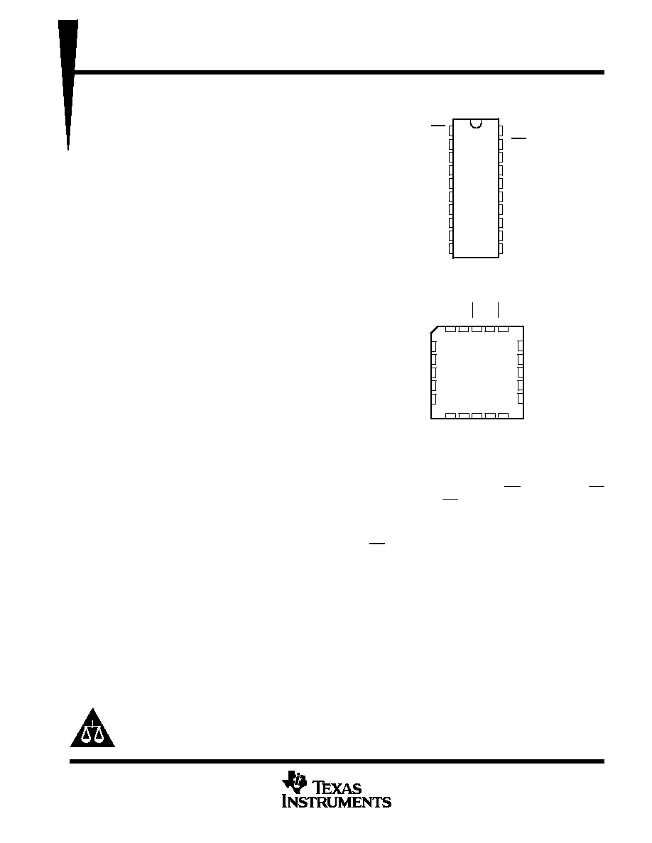
SN54LVT240A . . . J PACKAGE
SN74LVT240A . . . DB, DW, OR PW PACKAGE
(TOP VIEW)
SN54LVT240A . . . FK PACKAGE
(TOP VIEW)
1
2
3
4
5
6
7
8
9
10
20
19
18
17
16
15
14
13
12
11
1OE
1A1
2Y4
1A2
2Y3
1A3
2Y2
1A4
2Y1
GND
V
CC
2OE
1Y1
2A4
1Y2
2A3
1Y3
2A2
1Y4
2A1
3
2
1 20 19
9 10 11 12 13
4
5
6
7
8
18
17
16
15
14
1Y1
2A4
1Y2
2A3
1Y3
1A2
2Y3
1A3
2Y2
1A4
2Y4
1A1
1OE
1Y4
2A2
2OE
2Y1
GND
2A1
V
CC
SN54LVT240A, SN74LVT240A
3.3-V ABT OCTAL BUFFERS/DRIVERS
WITH 3-STATE OUTPUTS
SCBS134I ≠ SEPTEMBER 1992 ≠ REVISED APRIL 2000
2
POST OFFICE BOX 655303
∑
DALLAS, TEXAS 75265
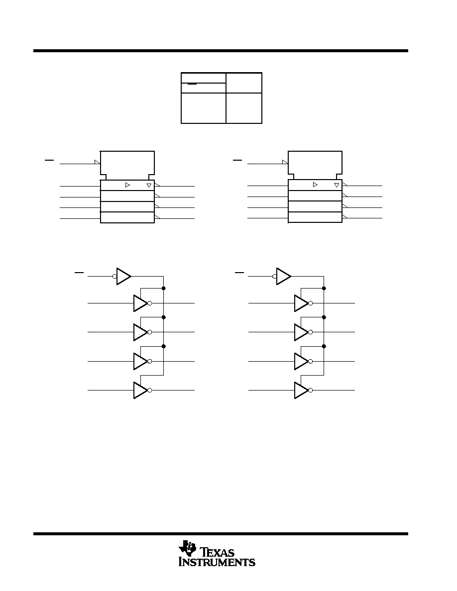
FUNCTION TABLE
(each 4-bit buffer)
INPUTS
OUTPUT
OE
A
Y
L
H
L
L
L
H
H
X
Z
logic symbol
2
1A1
4
1A2
6
1A3
8
1A4
EN
1
1Y1
18
1Y2
16
1Y3
14
1Y4
12
11
2A1
13
2A2
15
2A3
17
2A4
2Y1
9
2Y2
7
2Y3
5
2Y4
3
1OE
This symbol is in accordance with ANSI/IEEE Std 91-1984 and IEC Publication 617-12.
2OE
EN
19
logic diagram (positive logic)
1
2
18
1Y1
1OE
1A1
4
16
1Y2
1A2
6
14
1Y3
1A3
8
12
1Y4
1A4
19
11
9
2Y1
2OE
2A1
13
7
2Y2
2A2
15
5
2Y3
2A3
17
3
2Y4
2A4
SN54LVT240A, SN74LVT240A
3.3-V ABT OCTAL BUFFERS/DRIVERS
WITH 3-STATE OUTPUTS
SCBS134I ≠ SEPTEMBER 1992 ≠ REVISED APRIL 2000
3
POST OFFICE BOX 655303
∑
DALLAS, TEXAS 75265
absolute maximum ratings over operating free-air temperature range (unless otherwise noted)
Supply voltage range, V
CC
≠0.5 V to 4.6 V
. . . . . . . . . . . . . . . . . . . . . . . . . . . . . . . . . . . . . . . . . . . . . . . . . . . . . . . . .
Input voltage range, V
I
(see Note 1)
≠0.5 V to 7 V
. . . . . . . . . . . . . . . . . . . . . . . . . . . . . . . . . . . . . . . . . . . . . . . . . .
Voltage range applied to any output in the high-impedance
or power-off state, V
O
(see Note 1)
≠0.5 V to 7 V
. . . . . . . . . . . . . . . . . . . . . . . . . . . . . . . . . . . . . . . . . . . . . . . .
Voltage range applied to any output in the high state, V
O
(see Note 1)
≠0.5 V to V
CC
+ 0.5 V
. . . . . . . . . . . . .
Current into any output in the low state, I
O
: SN54LVT240A 96
mA
. . . . . . . . . . . . . . . . . . . . . . . . . . . . . . . . . . .
SN74LVT240A
128 mA
. . . . . . . . . . . . . . . . . . . . . . . . . . . . . . . . . . .
Current into any output in the high state, I
O
(see Note 2): SN54LVT240A
48 mA
. . . . . . . . . . . . . . . . . . . . . . . .
SN74LVT240A
64 mA
. . . . . . . . . . . . . . . . . . . . . . . .
Input clamp current, I
IK
(V
I
< 0)
≠50 mA
. . . . . . . . . . . . . . . . . . . . . . . . . . . . . . . . . . . . . . . . . . . . . . . . . . . . . . . . . . .
Output clamp current, I
OK
(V
O
< 0)
≠50 mA
. . . . . . . . . . . . . . . . . . . . . . . . . . . . . . . . . . . . . . . . . . . . . . . . . . . . . . . .
Package thermal impedance,
JA
(see Note 3): DB package
70
∞
C/W
. . . . . . . . . . . . . . . . . . . . . . . . . . . . . . . . .
DW package
58
∞
C/W
. . . . . . . . . . . . . . . . . . . . . . . . . . . . . . . . .
PW package
83
∞
C/W
. . . . . . . . . . . . . . . . . . . . . . . . . . . . . . . . .
Storage temperature range, T
stg
≠65
∞
C to 150
∞
C
. . . . . . . . . . . . . . . . . . . . . . . . . . . . . . . . . . . . . . . . . . . . . . . . . . .
Stresses beyond those listed under "absolute maximum ratings" may cause permanent damage to the device. These are stress ratings only, and
functional operation of the device at these or any other conditions beyond those indicated under "recommended operating conditions" is not
implied. Exposure to absolute-maximum-rated conditions for extended periods may affect device reliability.
NOTES:
1. The input and output negative-voltage ratings may be exceeded if the input and output clamp-current ratings are observed.
2. This current flows only when the output is in the high state and VO > VCC.
3. The package thermal impedance is calculated in accordance with JESD 51.
recommended operating conditions (see Note 4)
SN54LVT240A
SN74LVT240A
UNIT
MIN
MAX
MIN
MAX
UNIT
VCC
Supply voltage
2.7
3.6
2.7
3.6
V
VIH
High-level input voltage
2
2
V
VIL
Low-level input voltage
0.8
0.8
V
VI
Input voltage
5.5
5.5
V
IOH
High-level output current
≠24
≠32
mA
IOL
Low-level output current
48
64
mA
t/
v
Input transition rise or fall rate
Outputs enabled
5
5
ns/V
t/
VCC
Power-up ramp rate
200
200
µ
s/V
TA
Operating free-air temperature
≠55
125
≠40
85
∞
C
NOTE 4: All unused inputs of the device must be held at VCC or GND to ensure proper device operation. Refer to the TI application report,
Implications of Slow or Floating CMOS Inputs, literature number SCBA004.
PRODUCT PREVIEW information concerns products in the formative or
design phase of development. Characteristic data and other
specifications are design goals. Texas Instruments reserves the right to
change or discontinue these products without notice.
SN54LVT240A, SN74LVT240A
3.3-V ABT OCTAL BUFFERS/DRIVERS
WITH 3-STATE OUTPUTS
SCBS134I ≠ SEPTEMBER 1992 ≠ REVISED APRIL 2000
4
POST OFFICE BOX 655303
∑
DALLAS, TEXAS 75265
electrical characteristics over recommended operating free-air temperature range (unless
otherwise noted)
PARAMETER
TEST CONDITIONS
SN54LVT240A
SN74LVT240A
UNIT
PARAMETER
TEST CONDITIONS
MIN
TYP
MAX
MIN
TYP
MAX
UNIT
VIK
VCC = 2.7 V,
II = ≠18 mA
≠1.2
≠1.2
V
VCC = 2.7 V to 3.6 V,
IOH = ≠100
µ
A
VCC≠0.2
VCC≠0.2
VOH
VCC = 2.7 V,
IOH = ≠8 mA
2.4
2.4
V
VOH
VCC = 3 V
IOH = ≠24 mA
2
V
VCC = 3 V
IOH = ≠32 mA
2
VCC = 2 7 V
IOL = 100
µ
A
0.2
0.2
VCC = 2.7 V
IOL = 24 mA
0.5
0.5
VOL
IOL = 16 mA
0.4
0.4
V
VOL
VCC = 3 V
IOL = 32 mA
0.5
0.5
V
VCC = 3 V
IOL = 48 mA
0.55
IOL = 64 mA
0.55
VCC = 0 or 3.6 V,
VI = 5.5 V
10
10
II
Control inputs
VCC = 3.6 V,
VI = VCC or GND
±
1
±
1
µ
A
II
Data inputs
VCC = 3 6 V
VI = VCC
1
1
µ
A
Data inputs
VCC = 3.6 V
VI = 0
≠5
≠5
Ioff
VCC = 0,
VI or VO = 0 to 4.5 V
±
100
µ
A
IOZPU
VCC = 0 to 1.5 V, VO = 0.5 V to 3 V,
OE = don't care
±
100*
±
100
µ
A
IOZPD
VCC = 1.5 V to 0, VO = 0.5 V to 3 V,
OE = don't care
±
100*
±
100
µ
A
IOZH
VCC = 3.6 V,
VO = 3 V
5
5
µ
A
IOZL
VCC = 3.6 V,
VO = 0.5 V
≠5
≠5
µ
A
VCC = 3.6 V,
Outputs high
0.19
0.19
ICC
VCC = 3.6 V,
IO = 0,
Outputs low
5
5
mA
VI = VCC or GND
Outputs disabled
0.19
0.19
ICC
VCC = 3 V to 3.6 V, One input at VCC ≠ 0.6 V,
Other inputs at VCC or GND
0.2
0.2
mA
Ci
VI = 3 V or 0
4
4
pF
Co
VO = 3 V or 0
7
7
pF
On products compliant to MIL-PRF-38535, this parameter is not production tested.
All typical values are at VCC = 3.3 V, TA = 25
∞
C.
This is the increase in supply current for each input that is at the specified TTL-voltage level rather than VCC or GND.
PRODUCT PREVIEW information concerns products in the formative or
design phase of development. Characteristic data and other
specifications are design goals. Texas Instruments reserves the right to
change or discontinue these products without notice.
SN54LVT240A, SN74LVT240A
3.3-V ABT OCTAL BUFFERS/DRIVERS
WITH 3-STATE OUTPUTS
SCBS134I ≠ SEPTEMBER 1992 ≠ REVISED APRIL 2000
5
POST OFFICE BOX 655303
∑
DALLAS, TEXAS 75265
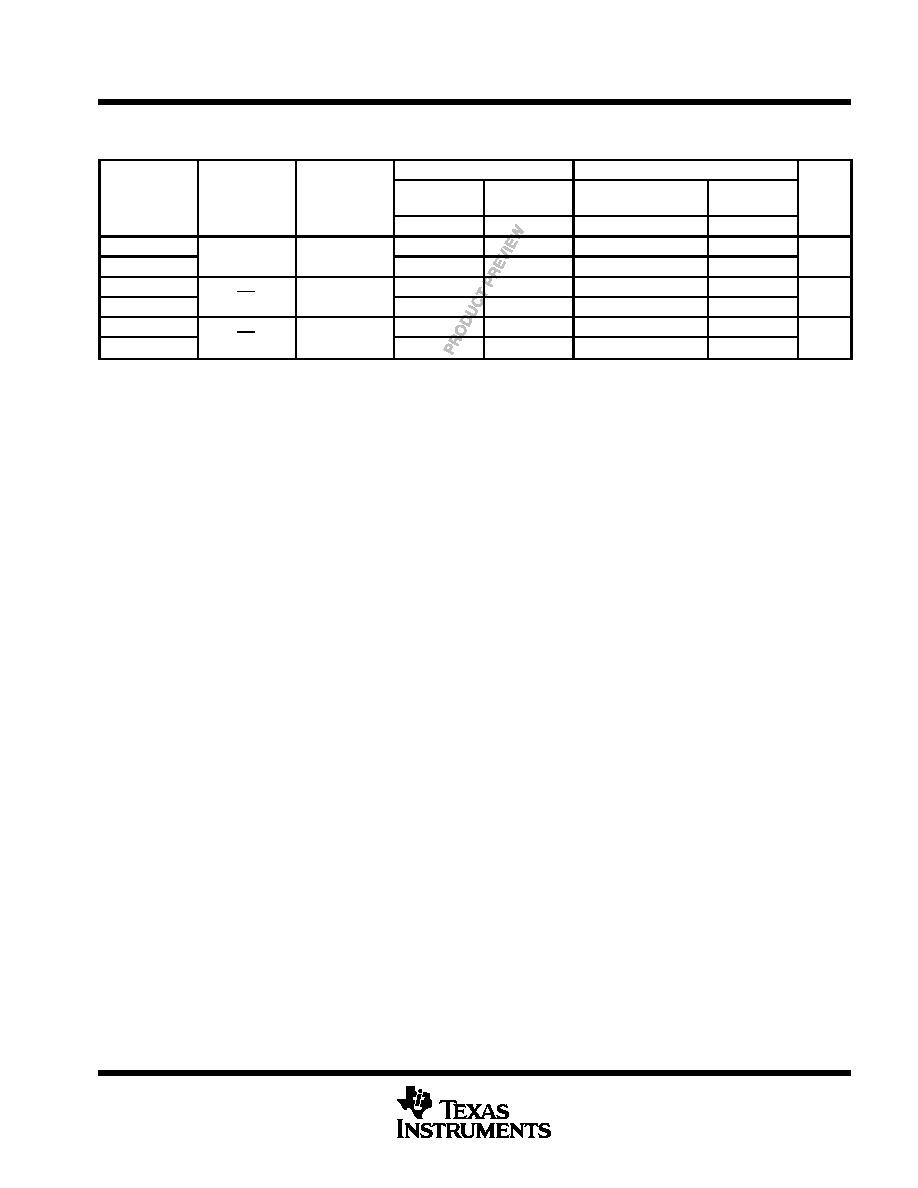
switching characteristics over recommended ranges of supply voltage and operating free-air
temperature, C
L
= 50 pF (unless otherwise noted) (see Figure 1)
SN54LVT240A
SN74LVT240A
PARAMETER
FROM
(INPUT)
TO
(OUTPUT)
VCC = 3.3 V
±
0.3 V
VCC = 2.7 V
VCC = 3.3 V
±
0.3 V
VCC = 2.7 V
UNIT
MIN
MAX
MIN
MAX
MIN
TYP
MAX
MIN
MAX
tPLH
A
Y
1
3.9
4.7
1.1
2.2
3.8
4.6
ns
tPHL
A
Y
1.2
4.2
4.3
1.3
2.6
4
4.2
ns
tPZH
OE
Y
1
4.7
5.7
1.1
2.6
4.6
5.6
ns
tPZL
OE
Y
1.3
4.6
5.2
1.4
2.7
4.4
5
ns
tPHZ
OE
Y
1.9
4.6
4.8
2
2.9
4.4
4.6
ns
tPLZ
OE
Y
1.7
4.7
4.7
1.8
3
4.3
4.3
ns
All typical values are at VCC = 3.3 V, TA = 25
∞
C.
PRODUCT PREVIEW information concerns products in the formative or
design phase of development. Characteristic data and other
specifications are design goals. Texas Instruments reserves the right to
change or discontinue these products without notice.