SN54LVTH540, SN74LVTH540
3.3-V ABT OCTAL BUFFERS/DRIVERS
WITH 3-STATE OUTPUTS
SCBS681E ≠ MARCH 1997 ≠ REVISED APRIL 1999
1
POST OFFICE BOX 655303
∑
DALLAS, TEXAS 75265
D
State-of-the-Art Advanced BiCMOS
Technology (ABT) Design for 3.3-V
Operation and Low Static-Power
Dissipation
D
I
off
and Power-Up 3-State Support Hot
Insertion
D
Bus Hold on Data Inputs Eliminates the
Need for External Pullup/Pulldown
Resistors
D
Support Mixed-Mode Signal Operation (5-V
Input and Output Voltages With 3.3-V V
CC
)
D
Support Unregulated Battery Operation
Down to 2.7 V
D
Typical V
OLP
(Output Ground Bounce)
< 0.8 V at V
CC
= 3.3 V, T
A
= 25
∞
C
D
Latch-Up Performance Exceeds 500 mA Per
JESD 17
D
ESD Protection Exceeds 2000 V Per
MIL-STD-883, Method 3015; Exceeds 200 V
Using Machine Model (C = 200 pF, R = 0)
D
Package Options Include Plastic
Small-Outline (DW), Shrink Small-Outline
(DB), and Thin Shrink Small-Outline (PW)
Packages, Ceramic Chip Carriers (FK),
Ceramic Flat (W) Package, and Ceramic (J)
DIPs
description
These octal buffers/drivers are designed specifically for low-voltage (3.3-V) V
CC
operation, but with the
capability to provide a TTL interface to a 5-V system environment.
The 'LVTH540 devices are ideal for driving bus lines or buffer memory address registers. These devices feature
inputs and outputs on opposite sides of the package that facilitate printed circuit board layout.
The 3-state control gate is a 2-input AND gate with active-low inputs so that if either output-enable (OE1 or OE2)
input is high, all outputs are in the high-impedance state.
Active bus-hold circuitry is provided to hold unused or floating data inputs at a valid logic level.
When V
CC
is between 0 and 1.5 V, the devices are in the high-impedance state during power up or power down.
However, to ensure the high-impedance state above 1.5 V, OE should be tied to V
CC
through a pullup resistor;
the minimum value of the resistor is determined by the current-sinking capability of the driver.
These devices are fully specified for hot-insertion applications using I
off
and power-up 3-state. The I
off
circuitry
disables the outputs, preventing damaging current backflow through the devices when they are powered down.
The power-up 3-state circuitry places the outputs in the high-impedance state during power up and power down,
which prevents driver conflict.
Copyright
©
1999, Texas Instruments Incorporated
UNLESS OTHERWISE NOTED this document contains PRODUCTION
DATA information current as of publication date. Products conform to
specifications per the terms of Texas Instruments standard warranty.
Production processing does not necessarily include testing of all
parameters.
Please be aware that an important notice concerning availability, standard warranty, and use in critical applications of
Texas Instruments semiconductor products and disclaimers thereto appears at the end of this data sheet.
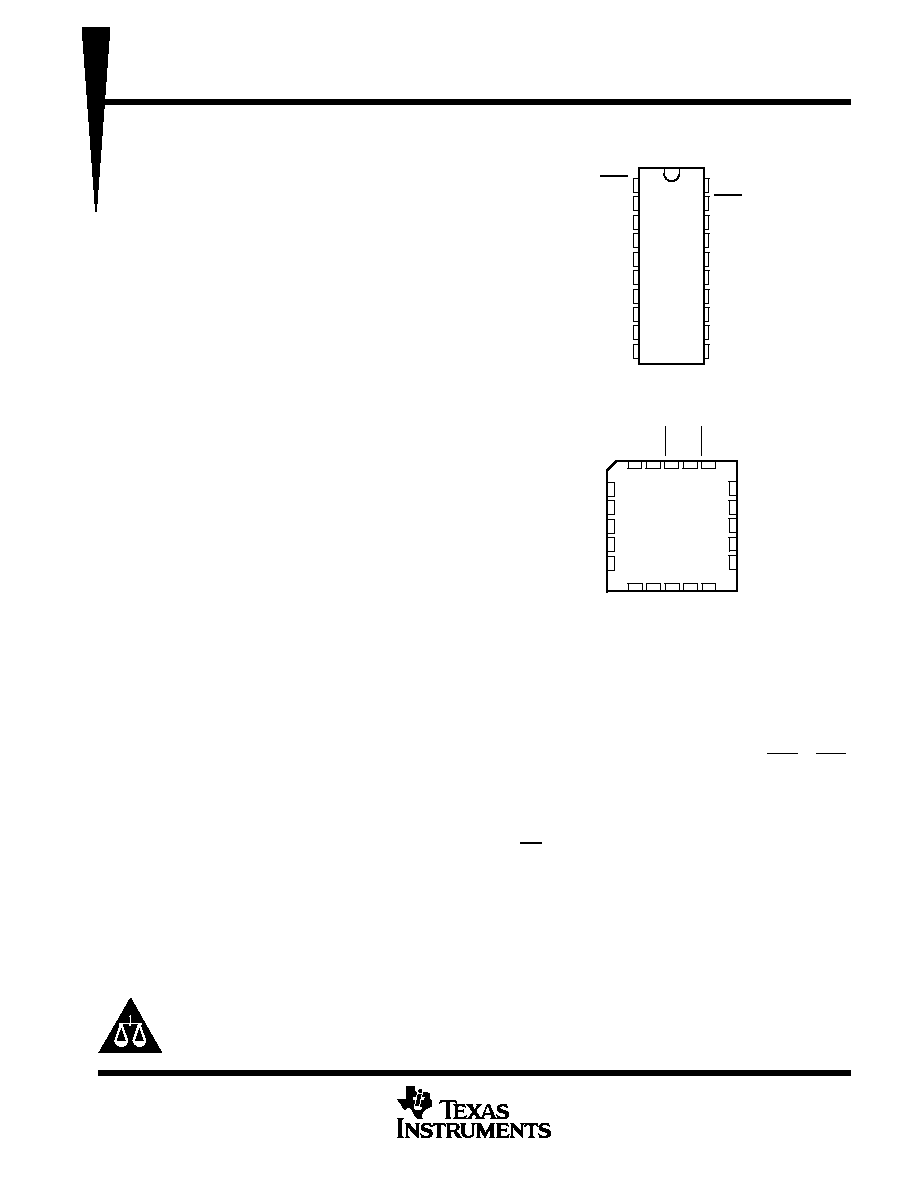
1
2
3
4
5
6
7
8
9
10
20
19
18
17
16
15
14
13
12
11
OE1
A1
A2
A3
A4
A5
A6
A7
A8
GND
V
CC
OE2
Y1
Y2
Y3
Y4
Y5
Y6
Y7
Y8
SN54LVTH540 . . . J OR W PACKAGE
SN74LVTH540 . . . DB, DW, OR PW PACKAGE
(TOP VIEW)
3
2
1 20 19
9 10 11 12 13
4
5
6
7
8
18
17
16
15
14
Y1
Y2
Y3
Y4
Y5
A3
A4
A5
A6
A7
SN54LVTH540 . . . FK PACKAGE
(TOP VIEW)
A2
A1
OE1
Y7
Y6
OE2
A8
GND
Y8
V
CC
SN54LVTH540, SN74LVTH540
3.3-V ABT OCTAL BUFFERS/DRIVERS
WITH 3-STATE OUTPUTS
SCBS681E ≠ MARCH 1997 ≠ REVISED APRIL 1999
2
POST OFFICE BOX 655303
∑
DALLAS, TEXAS 75265
description (continued)
The SN54LVTH540 is characterized for operation over the full military temperature range of ≠55
∞
C to 125
∞
C.
The SN74LVTH540 is characterized for operation from ≠40
∞
C to 85
∞
C.
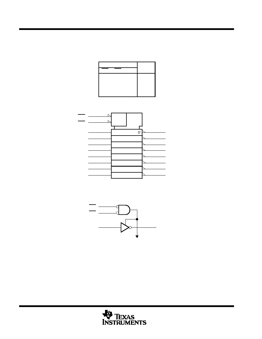
FUNCTION TABLE
INPUTS
OUTPUT
OE1
OE2
A
Y
L
L
L
H
L
L
H
L
H
X
X
Z
X
H
X
Z
logic symbol
2
A1
3
A2
4
A3
1
Y1
18
Y2
17
Y3
16
&
EN
5
A4
6
A5
7
A6
Y4
15
Y5
14
Y6
13
19
OE1
OE2
8
A7
9
A8
Y7
12
Y8
11
This symbol is in accordance with ANSI/IEEE Std 91-1984 and IEC Publication 617-12.
1
logic diagram (positive logic)
OE1
OE2
To Seven Other Channels
A1
Y1
1
19
2
18
SN54LVTH540, SN74LVTH540
3.3-V ABT OCTAL BUFFERS/DRIVERS
WITH 3-STATE OUTPUTS
SCBS681E ≠ MARCH 1997 ≠ REVISED APRIL 1999
3
POST OFFICE BOX 655303
∑
DALLAS, TEXAS 75265
absolute maximum ratings over operating free-air temperature range (unless otherwise noted)
Supply voltage range, V
CC
≠0.5 V to 4.6 V
. . . . . . . . . . . . . . . . . . . . . . . . . . . . . . . . . . . . . . . . . . . . . . . . . . . . . . . . .
Input voltage range, V
I
(see Note 1)
≠0.5 V to 7 V
. . . . . . . . . . . . . . . . . . . . . . . . . . . . . . . . . . . . . . . . . . . . . . . . . .
Voltage range applied to any output in the high-impedance
or power-off state, V
O
(see Note 1)
≠0.5 V to 7 V
. . . . . . . . . . . . . . . . . . . . . . . . . . . . . . . . . . . . . . . . . . . . . . . .
Voltage range applied to any output in the high state, V
O
(see Note 1)
≠0.5 V to V
CC
+ 0.5 V
. . . . . . . . . . . . .
Current into any output in the low state, I
O
: SN54LVTH540 96
mA
. . . . . . . . . . . . . . . . . . . . . . . . . . . . . . . . . . .
SN74LVTH540 128
mA
. . . . . . . . . . . . . . . . . . . . . . . . . . . . . . . . . .
Current into any output in the high state, I
O
(see Note 2): SN54LVTH540
48 mA
. . . . . . . . . . . . . . . . . . . . . . .
SN74LVTH540 64
mA
. . . . . . . . . . . . . . . . . . . . . . .
Input clamp current, I
IK
(V
I
< 0)
≠50 mA
. . . . . . . . . . . . . . . . . . . . . . . . . . . . . . . . . . . . . . . . . . . . . . . . . . . . . . . . . . .
Output clamp current, I
OK
(V
O
< 0)
≠50 mA
. . . . . . . . . . . . . . . . . . . . . . . . . . . . . . . . . . . . . . . . . . . . . . . . . . . . . . . .
Package thermal impedance,
JA
(see Note 3): DB package
115
∞
C/W
. . . . . . . . . . . . . . . . . . . . . . . . . . . . . . . .
DW package
97
∞
C/W
. . . . . . . . . . . . . . . . . . . . . . . . . . . . . . . . .
PW package
128
∞
C/W
. . . . . . . . . . . . . . . . . . . . . . . . . . . . . . . .
Storage temperature range, T
stg
≠65
∞
C to 150
∞
C
. . . . . . . . . . . . . . . . . . . . . . . . . . . . . . . . . . . . . . . . . . . . . . . . . . .
Stresses beyond those listed under "absolute maximum ratings" may cause permanent damage to the device. These are stress ratings only, and
functional operation of the device at these or any other conditions beyond those indicated under "recommended operating conditions" is not
implied. Exposure to absolute-maximum-rated conditions for extended periods may affect device reliability.
NOTES:
1. The input and output negative-voltage ratings may be exceeded if the input and output clamp-current ratings are observed.
2. This current flows only when the output is in the high state and VO > VCC.
3. The package thermal impedance is calculated in accordance with JESD 51.
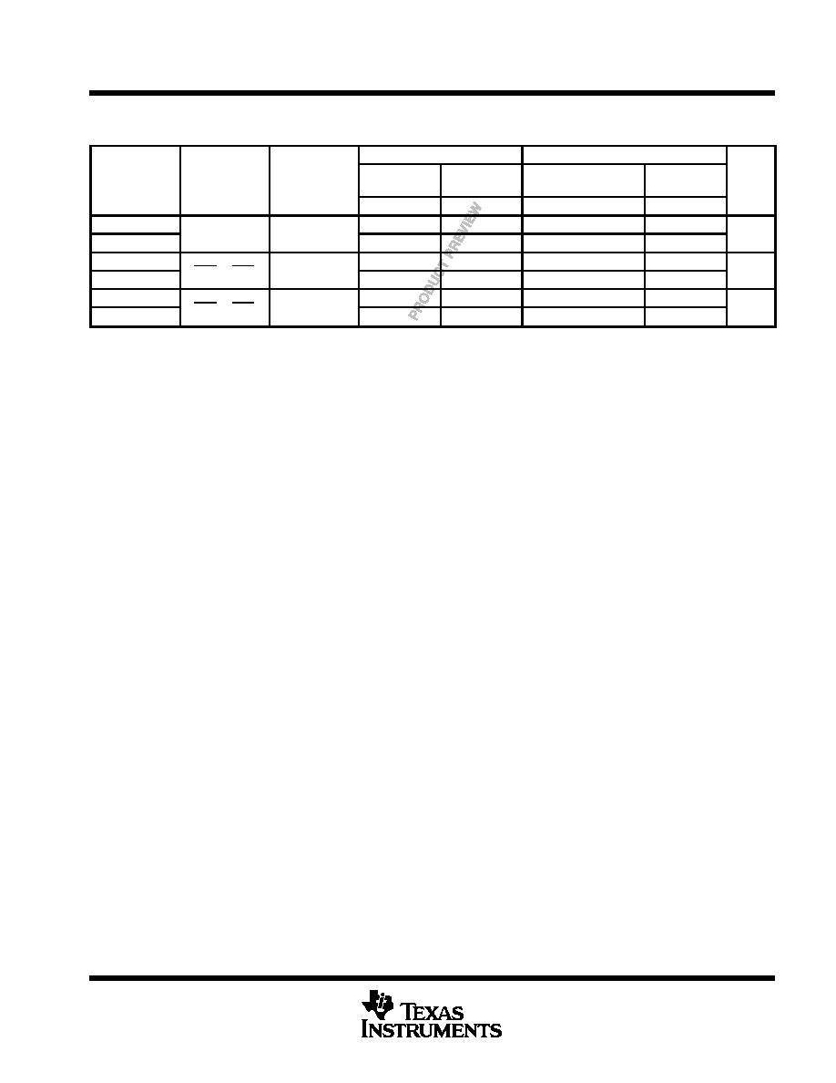
recommended operating conditions (see Note 4)
SN54LVTH540
SN74LVTH540
UNIT
MIN
MAX
MIN
MAX
UNIT
VCC
Supply voltage
2.7
3.6
2.7
3.6
V
VIH
High-level input voltage
2
2
V
VIL
Low-level input voltage
0.8
0.8
V
VI
Input voltage
5.5
5.5
V
IOH
High-level output current
≠24
≠32
mA
IOL
Low-level output current
48
64
mA
t/
v
Input transition rise or fall rate
10
10
ns/V
t/
VCC
Power-up ramp rate
200
200
µ
s/V
TA
Operating free-air temperature
≠55
125
≠40
85
∞
C
NOTE 4: All unused control inputs of the device must be held at VCC or GND to ensure proper device operation. Refer to the TI application report,
Implications of Slow or Floating CMOS Inputs, literature number SCBA004.
PRODUCT PREVIEW information concerns products in the formative or
design phase of development. Characteristic data and other
specifications are design goals. Texas Instruments reserves the right to
change or discontinue these products without notice.
SN54LVTH540, SN74LVTH540
3.3-V ABT OCTAL BUFFERS/DRIVERS
WITH 3-STATE OUTPUTS
SCBS681E ≠ MARCH 1997 ≠ REVISED APRIL 1999
4
POST OFFICE BOX 655303
∑
DALLAS, TEXAS 75265
electrical characteristics over recommended operating free-air temperature range (unless
otherwise noted)
PARAMETER
TEST CONDITIONS
SN54LVTH540
SN74LVTH540
UNIT
PARAMETER
TEST CONDITIONS
MIN
TYP
MAX
MIN
TYP
MAX
UNIT
VIK
VCC = 2.7 V,
II = ≠18 mA
≠1.2
≠1.2
V
VCC = 2.7 V to 3.6 V,
IOH = ≠100
µ
A
VCC≠0.2
VCC≠0.2
VOH
VCC = 2.7 V,
IOH = ≠8 mA
2.4
2.4
V
VOH
VCC = 3 V
IOH = ≠24 mA
2
V
VCC = 3 V
IOH = ≠32 mA
2
VCC = 2 7 V
IOL = 100
µ
A
0.2
0.2
VCC = 2.7 V
IOL = 24 mA
0.5
0.5
VOL
IOL = 16 mA
0.4
0.4
V
VOL
VCC = 3 V
IOL = 32 mA
0.5
0.5
V
VCC = 3 V
IOL = 48 mA
0.55
IOL = 64 mA
0.55
VCC = 0 or 3.6 V,
VI = 5.5 V
10
10
II
Control inputs
VCC = 3.6 V,
VI = VCC or GND
±
1
±
1
µ
A
II
Data inp ts
VCC = 3 6 V
VI = VCC
1
1
µ
A
Data inputs
VCC = 3.6 V
VI = 0
≠5
≠5
Ioff
VCC = 0,
VI or VO = 0 to 4.5 V
±
100
µ
A
VCC = 3 V
VI = 0.8 V
75
75
II(hold) Data inputs
VCC = 3 V
VI = 2 V
≠75
≠75
µ
A
(
)
VCC = 3.6 V,
VI = 0 to 3.6 V
±
500
IOZH
VCC = 3.6 V,
VO = 3 V
5
5
µ
A
IOZL
VCC = 3.6 V,
VO = 0.5 V
≠5
≠5
µ
A
IOZPU
VCC = 0 to 1.5 V, VO = 0.5 V to 3 V,
OE = don't care
±
100
±
100
µ
A
IOZPD
VCC = 1.5 V to 0, VO = 0.5 V to 3 V,
OE = don't care
±
100
±
100
µ
A
VCC = 3.6 V,
Outputs high
0.19
0.19
ICC
VCC = 3.6 V,
IO = 0,
Outputs low
5
5
mA
VI = VCC or GND
Outputs disabled
0.19
0.19
ICCß
VCC = 3 V to 3.6 V, One input at VCC ≠ 0.6 V,
Other inputs at VCC or GND
0.2
0.2
mA
Ci
VI = 3 V or 0
3
3
pF
Co
VO = 3 V or 0
7
7
pF
On products compliant to MIL-PRF-38535, this parameter is not production tested.
All typical values are at VCC = 3.3 V, TA = 25
∞
C.
This is the bus-hold maximum dynamic current. It is the minimum overdrive current required to switch the input from one state to another.
ß This is the increase in supply current for each input that is at the specified TTL voltage level rather than VCC or GND.
PRODUCT PREVIEW information concerns products in the formative or
design phase of development. Characteristic data and other
specifications are design goals. Texas Instruments reserves the right to
change or discontinue these products without notice.
SN54LVTH540, SN74LVTH540
3.3-V ABT OCTAL BUFFERS/DRIVERS
WITH 3-STATE OUTPUTS
SCBS681E ≠ MARCH 1997 ≠ REVISED APRIL 1999
5
POST OFFICE BOX 655303
∑
DALLAS, TEXAS 75265
switching characteristics over recommended ranges of supply voltage and operating free-air
temperature, C
L
= 50 pF (unless otherwise noted) (see Figure 1)
SN54LVTH540
SN74LVTH540
PARAMETER
FROM
(INPUT)
TO
(OUTPUT)
VCC = 3.3 V
±
0.3 V
VCC = 2.7 V
VCC = 3.3 V
±
0.3 V
VCC = 2.7 V
UNIT
MIN
MAX
MIN
MAX
MIN
TYP
MAX
MIN
MAX
tPLH
A
Y
1
3.9
4.7
1.1
2.4
3.8
4.6
ns
tPHL
A
Y
1
3.9
4.7
1.1
2.7
3.8
4.6
ns
tPZH
OE1 or OE2
Y
1.4
5.3
6.3
1.5
3.4
5.2
6.2
ns
tPZL
OE1 or OE2
Y
1.4
5.5
6.1
1.5
3.7
5.3
5.9
ns
tPHZ
OE1 or OE2
Y
1.4
5.9
6.2
1.5
3.9
5.6
5.9
ns
tPLZ
OE1 or OE2
Y
1.4
5.5
5.8
1.5
3.5
5
5.3
ns
All typical values are at VCC = 3.3 V, TA = 25
∞
C.
PRODUCT PREVIEW information concerns products in the formative or
design phase of development. Characteristic data and other
specifications are design goals. Texas Instruments reserves the right to
change or discontinue these products without notice.