SN54LVTZ245, SN74LVTZ245
3.3-V ABT OCTAL BUS TRANSCEIVERS
WITH 3-STATE OUTPUTS
SCBS303C ≠ DECEMBER 1993 ≠ REVISED JANUARY 1996
1
POST OFFICE BOX 655303
∑
DALLAS, TEXAS 75265
D
State-of-the-Art Advanced BiCMOS
Technology (ABT) Design for 3.3-V
Operation and Low-Static Power
Dissipation
D
High-Impedance State During Power Up
and Power Down
D
Support Mixed-Mode Signal Operation (5-V
Input and Output Voltages With 3.3-V V
CC
)
D
Support Unregulated Battery Operation
Down to 2.7 V
D
Typical V
OLP
(Output Ground Bounce)
< 0.8 V at V
CC
= 3.3 V, T
A
= 25
∞
C
D
Latch-Up Performance Exceeds 500 mA
Per JEDEC Standard JESD-17
D
Bus-Hold Data Inputs Eliminate the Need
for External Pullup/Pulldown Resistors
D
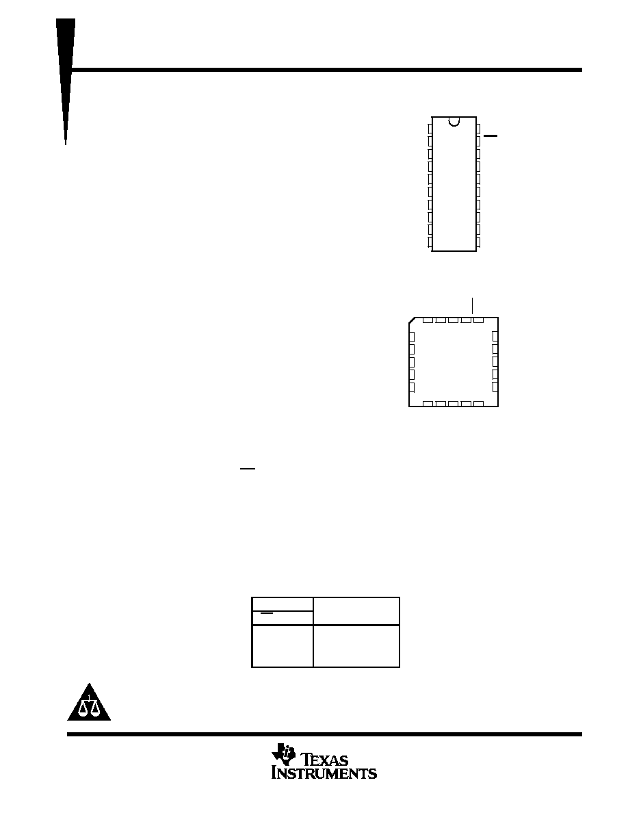
Package Options Include Plastic
Small-Outline (DW), Shrink Small-Outline
(DB), and Thin Shrink Small-Outline (PW)
Packages, Ceramic Chip Carriers (FK), and
Ceramic (J) DIPs
description
These octal bus transceivers are designed
specifically for low-voltage (3.3-V) V
CC
operation,
but with the capability to provide a TTL interface
to a 5-V system environment.
These devices are designed for asynchronous communication between data buses. They transmit data from
the A bus to the B bus or from the B bus to the A bus, depending upon the logic level at the direction-control
(DIR) input. The output-enable (OE) input can be used to disable the devices so the buses are effectively
isolated.
Active bus-hold circuitry is provided to hold unused or floating data inputs at a valid logic level.
The SN74LVTZ245 is available in TI's shrink small-outline package (DB), which provides the same I/O pin count
and functionality of standard small-outline packages in less than half the printed-circuit-board area.
The SN54LVTZ245 is characterized for operation over the full military temperature range of ≠ 55
∞
C to 125
∞
C.
The SN74LVTZ245 is characterized for operation from ≠ 40
∞
C to 85
∞
C.
FUNCTION TABLE
INPUTS
OPERATION
OE
DIR
OPERATION
L
L
B data to A bus
L
H
A data to B bus
H
X
Isolation
Copyright
©
1996, Texas Instruments Incorporated
PRODUCTION DATA information is current as of publication date.
Products conform to specifications per the terms of Texas Instruments
standard warranty. Production processing does not necessarily include
testing of all parameters.
1
2
3
4
5
6
7
8
9
10
20
19
18
17
16
15
14
13
12
11
DIR
A1
A2
A3
A4
A5
A6
A7
A8
GND
V
CC
OE
B1
B2
B3
B4
B5
B6
B7
B8
SN54LVTZ245 . . . J PACKAGE
SN74LVTZ245 . . . DB, DW, OR PW PACKAGE
(TOP VIEW)
3
2
1 20 19
9 10 11 12 13
4
5
6
7
8
18
17
16
15
14
B1
B2
B3
B4
B5
A3
A4
A5
A6
A7
A2
A1
DIR
B7
B6
OE
A8
GND
B8
V
CC
SN54LVTZ245 . . . FK PACKAGE
(TOP VIEW)
Please be aware that an important notice concerning availability, standard warranty, and use in critical applications of
Texas Instruments semiconductor products and disclaimers thereto appears at the end of this data sheet.
SN54LVTZ245, SN74LVTZ245
3.3-V ABT OCTAL BUS TRANSCEIVERS
WITH 3-STATE OUTPUTS
SCBS303C ≠ DECEMBER 1993 ≠ REVISED JANUARY 1996
2
POST OFFICE BOX 655303
∑
DALLAS, TEXAS 75265
logic symbol
logic diagram (positive logic)
B2
17
B3
16
B4
15
A5
6
A6
7
A7
8
A8
9
A2
3
A3
4
A4
5
OE
A1
2
G3
19
3EN2[AB]
B5
14
B6
13
B7
12
B8
11
B1
18
3EN1[BA]
1
DIR
DIR
OE
A1
B1
1
2
18
19
To Seven Other Channels
1
2
This symbol is in accordance with ANSI/IEEE Std 91-1984
and IEC Publication 617-12.
Pin numbers shown are for the DB, DW, PW, and J packages.
absolute maximum ratings over operating free-air temperature range (unless otherwise noted)
Supply voltage range, V
CC
≠ 0.5 V to 4.6 V
. . . . . . . . . . . . . . . . . . . . . . . . . . . . . . . . . . . . . . . . . . . . . . . . . . . . . . . .
Input voltage range, V
I
(see Note 1)
≠ 0.5 V to 7 V
. . . . . . . . . . . . . . . . . . . . . . . . . . . . . . . . . . . . . . . . . . . . . . . . . .
Voltage range applied to any output in the high state or power-off state, V
O
(see Note 1)
≠ 0.5 V to 7 V
. . . .
Current into any output in the low state, I
O
: SN54LVTZ245
96 mA
. . . . . . . . . . . . . . . . . . . . . . . . . . . . . . . . . . . .
SN74LVTZ245
128 mA
. . . . . . . . . . . . . . . . . . . . . . . . . . . . . . . . . . .
Current into any output in the high state, I
O
(see Note 2): SN54LVTZ245
48 mA
. . . . . . . . . . . . . . . . . . . . . . . .
SN74LVTZ245
64 mA
. . . . . . . . . . . . . . . . . . . . . . . .
Input clamp current, I
IK
(V
I
< 0)
≠ 50 mA
. . . . . . . . . . . . . . . . . . . . . . . . . . . . . . . . . . . . . . . . . . . . . . . . . . . . . . . . . .
Output clamp current, I
OK
(V
O
< 0)
≠ 50 mA
. . . . . . . . . . . . . . . . . . . . . . . . . . . . . . . . . . . . . . . . . . . . . . . . . . . . . . .
Maximum power dissipation at T
A
= 55
∞
C (in still air) (see Note 3): DB package
0.6 W
. . . . . . . . . . . . . . . . . . . .
DW package
1.6 W
. . . . . . . . . . . . . . . . . . .
PW package
0.7 W
. . . . . . . . . . . . . . . . . . .
Storage temperature range, T
stg
≠ 65
∞
C to 150
∞
C
. . . . . . . . . . . . . . . . . . . . . . . . . . . . . . . . . . . . . . . . . . . . . . . . . .
Stresses beyond those listed under "absolute maximum ratings" may cause permanent damage to the device. These are stress ratings only, and
functional operation of the device at these or any other conditions beyond those indicated under "recommended operating conditions" is not
implied. Exposure to absolute-maximum-rated conditions for extended periods may affect device reliability.
NOTES:
1. The input and output negative-voltage ratings may be exceeded if the input and output clamp-current ratings are observed.
2. This current flows only when the output is in the high state and VO > VCC.
3. The maximum package power dissipation is calculated using a junction temperature of 150
∞
C and a board trace length of 750 mils.
For more information, refer to the
Package Thermal Considerations application note in the 1994 ABT Advanced BiCMOS Technology
Data Book, literature number SCBD002B.
SN54LVTZ245, SN74LVTZ245
3.3-V ABT OCTAL BUS TRANSCEIVERS
WITH 3-STATE OUTPUTS
SCBS303C ≠ DECEMBER 1993 ≠ REVISED JANUARY 1996
3
POST OFFICE BOX 655303
∑
DALLAS, TEXAS 75265
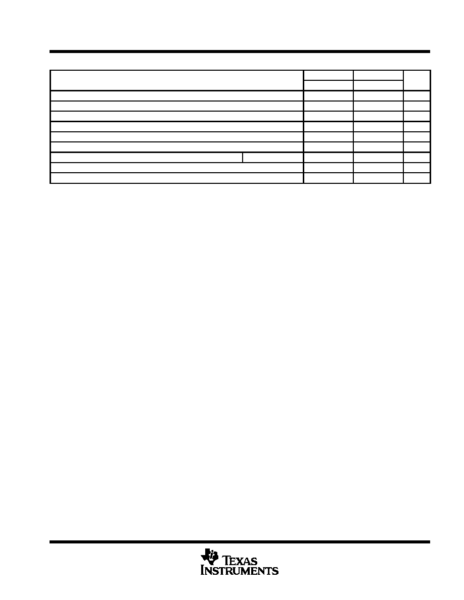
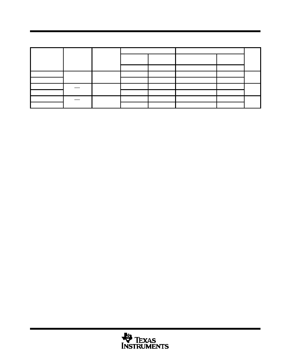
recommended operating conditions (see Note 4)
SN54LVTZ245
SN74LVTZ245
UNIT
MIN
MAX
MIN
MAX
UNIT
VCC
Supply voltage
2.7
3.6
2.7
3.6
V
VIH
High-level input voltage
2
2
V
VIL
Low-level input voltage
0.8
0.8
V
VI
Input voltage
5.5
5.5
V
IOH
High-level output current
≠24
≠32
mA
IOL
Low-level output current
48
64
mA
t /
v
Input transition rise or fall rate
Outputs enabled
10
10
ns / V
t /
VCC
Power-up ramp rate
200
200
µ
s / V
TA
Operating free-air temperature
≠55
125
≠40
85
∞
C
NOTE 4: Unused control inputs must be held high or low to prevent them from floating.
SN54LVTZ245, SN74LVTZ245
3.3-V ABT OCTAL BUS TRANSCEIVERS
WITH 3-STATE OUTPUTS
SCBS303C ≠ DECEMBER 1993 ≠ REVISED JANUARY 1996
4
POST OFFICE BOX 655303
∑
DALLAS, TEXAS 75265
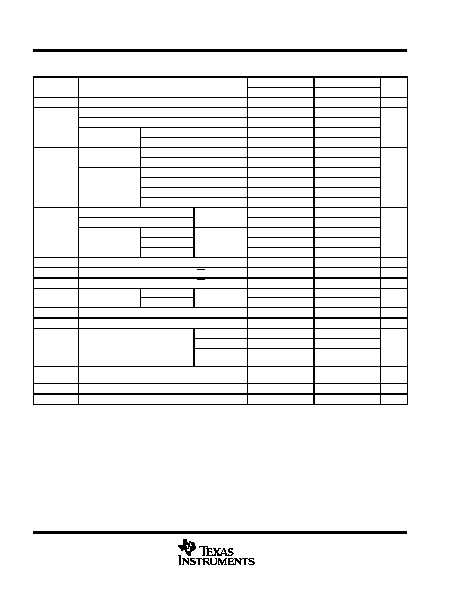
electrical characteristics over recommended operating free-air temperature range (unless
otherwise noted)
PARAMETER
TEST CONDITIONS
SN54LVTZ245
SN74LVTZ245
UNIT
PARAMETER
TEST CONDITIONS
MIN
TYP
MAX
MIN
TYP
MAX
UNIT
VIK
VCC = 2.7 V,
II = ≠18 mA
≠1.2
≠1.2
V
VCC = MIN to MAX, IOH = ≠100
µ
A
VCC ≠ 0.2
VCC ≠ 0.2
VOH
VCC = 2.7 V,
IOH = ≠ 8 mA
2.4
2.4
V
VOH
VCC = 3 V
IOH = ≠ 24 mA
2
V
VCC = 3 V
IOH = ≠ 32 mA
2
VCC = 2 7 V
IOL = 100
µ
A
0.2
0.2
VCC = 2.7 V
IOL = 24 mA
0.5
0.5
VOL
IOL = 16 mA
0.4
0.4
V
VOL
VCC = 3 V
IOL = 32 mA
0.5
0.5
V
VCC = 3 V
IOL = 48 mA
0.55
IOL = 64 mA
0.55
VCC = 3.6 V,
VI = VCC or GND
Control inputs
±
1
±
1
VCC = 0 or MAX,
VI = 5.5 V
Control inputs
10
10
II
VI = 5.5 V
ß
100
20
µ
A
VCC = 3.6 V
VI = VCC
A or B portsß
5
5
VI = 0
≠ 10
≠ 10
Ioff
VCC = 0,
VI or VO = 0 to 4.5 V
±
100
µ
A
IOZPU∂
VCC = 0 to 1.5 V,
VO = 0.5 V to 3 V, OE = X
±
50
µ
A
IOZPD∂
VCC = 1.5 V to 0,
VO = 0.5 V to 3 V, OE = X
±
50
µ
A
II(h ld)
VCC = 3 V
VI = 0.8 V
A or B ports
75
75
µ
A
II(hold)
VCC = 3 V
VI = 2 V
A or B ports
≠75
≠75
µ
A
IOZH
VCC = 3.6 V,
VO = 3 V
1
1
µ
A
IOZL
VCC = 3.6 V,
VO = 0.5 V
≠1
≠1
µ
A
Outputs high
0.13
0.5
0.13
0.225
ICC
VCC = 3.6 V,
IO = 0,
Outputs low
8.8
17
8.8
15
mA
ICC
VI = VCC or GND
Outputs
disabled
0.13
0.5
0.13
0.225
mA
ICC#
VCC = 3 V to 3.6 V,
One input at VCC ≠ 0.6 V,
Other inputs at VCC or GND
0.3
0.2
mA
Ci
VI = 3 V or 0
4
4
pF
Cio
VO = 3 V or 0
10
10
pF
All typical values are at VCC = 3.3 V, TA = 25
∞
C.
For conditions shown as MIN or MAX, use the appropriate value specified under recommended operating conditions.
ß Unused terminals at VCC or GND
∂ This parameter is specified by characterization but is not production tested.
# This is the increase in supply current for each input that is at the specified TTL voltage level rather than VCC or GND.
SN54LVTZ245, SN74LVTZ245
3.3-V ABT OCTAL BUS TRANSCEIVERS
WITH 3-STATE OUTPUTS
SCBS303C ≠ DECEMBER 1993 ≠ REVISED JANUARY 1996
5
POST OFFICE BOX 655303
∑
DALLAS, TEXAS 75265
switching characteristics over recommended operating free-air temperature range, C
L
= 50 pF
(unless otherwise noted) (see Figure 1)
SN54LVTZ245
SN74LVTZ245
PARAMETER
FROM
(INPUT)
TO
(OUTPUT)
VCC = 3.3 V
±
0.3 V
VCC = 2.7 V
VCC = 3.3 V
±
0.3 V
VCC = 2.7 V
UNIT
MIN
MAX
MIN
MAX
MIN
TYP
MAX
MIN
MAX
tPLH
A or B
B or A
1
4.6
5.3
1
2.5
4
5.2
ns
tPHL
A or B
B or A
1
4.1
5.7
1
2.5
4
5.5
ns
tPZH
OE
A or B
1.1
6.1
7.2
1.1
3.3
5.9
7.1
ns
tPZL
OE
A or B
1.5
6.6
8
1.5
3.8
6.5
7.9
ns
tPHZ
OE
A or B
2.2
6.2
7
2.2
4.3
5.9
6.5
ns
tPLZ
OE
A or B
2
5.7
5.9
2
3.9
5.5
5.6
ns
All typical values are at VCC = 3.3 V, TA = 25
∞
C.