SN74SSTVF32852
24-BIT TO 48-BIT REGISTERED BUFFER
WITH SSTL_2 INPUTS AND OUTPUTS
SCES426A ≠ FEBRUARY 2003 ≠ REVISED MARCH 2003
1
POST OFFICE BOX 655303
∑
DALLAS, TEXAS 75265
D
Member of the Texas Instruments
Widebus
Family
D
Operates at 2.3 V to 2.7 V for PC1600,
PC2100, and PC2700; 2.5 V to 2.7 V for
PC3200
D
Pinout and Functionality Compatible With
JEDEC Standard SSTV32852
D
Pinout Optimizes 1U DDR DIMM Layout
D
600 ps Faster (Simultaneous Switching)
Than the JEDEC Standard SSTV32852 in
PC2700 DIMM Applications
D
1-to-2 Outputs Support Stacked DDR
DIMMs
D
One Device Per DIMM Required
D
Output Edge-Control Circuitry Minimizes
Switching Noise in an Unterminated Line
D
Outputs Meet SSTL_2 Class I
Specifications
D
Supports SSTL_2 Data Inputs
D
Differential Clock (CLK and CLK) Inputs
D
Supports LVCMOS Switching Levels on the
RESET Input
D
RESET Input Disables Differential Input
Receivers, Resets All Registers, and
Forces All Outputs Low
D
Latch-Up Performance Exceeds 100 mA Per
JESD 78, Class II
D
ESD Protection Exceeds JESD 22
≠ 2000-V Human-Body Model (A114-A)
≠ 200-V Machine Model (A115-A)
≠ 1000-V Charged-Device Model (C101)
description/ordering information
This 24-bit to 48-bit registered buffer is designed for 2.3-V to 2.7-V V
CC
operation.
All inputs are SSTL_2, except the LVCMOS reset (RESET) input. All outputs are edge-controlled circuits,
optimized for unterminated DIMM loads, and meet SSTL_2 Class I specifications.
The SN74SSTVF32852 operates from a differential clock (CLK and CLK). Data are registered at the crossing
of CLK going high and CLK going low.
The device supports low-power standby operation. When RESET is low, the differential input receivers are
disabled, and undriven (floating) data, clock, and reference voltage (V
REF
) inputs are allowed. In addition, when
RESET is low, all registers are reset and all outputs are forced low. The LVCMOS RESET input always must
be held at a valid logic high or low level.
To ensure defined outputs from the register before a stable clock has been supplied, RESET must be held in
the low state during power up.
ORDERING INFORMATION
TA
PACKAGE
ORDERABLE
PART NUMBER
TOP-SIDE
MARKING
0
∞
C to 70
∞
C
LFBGA ≠ GKF
Tape and reel
SN74SSTVF32852KR
SVF852
Package drawings, standard packing quantities, thermal data, symbolization, and PCB design
guidelines are available at www.ti.com/sc/package.
Copyright
2003, Texas Instruments Incorporated
Widebus is a trademark of Texas Instruments.
Please be aware that an important notice concerning availability, standard warranty, and use in critical applications of
Texas Instruments semiconductor products and disclaimers thereto appears at the end of this data sheet.
PRODUCTION DATA information is current as of publication date.
Products conform to specifications per the terms of Texas Instruments
standard warranty. Production processing does not necessarily include
testing of all parameters.
SN74SSTVF32852
24-BIT TO 48-BIT REGISTERED BUFFER
WITH SSTL_2 INPUTS AND OUTPUTS
SCES426A ≠ FEBRUARY 2003 ≠ REVISED MARCH 2003
2
POST OFFICE BOX 655303
∑
DALLAS, TEXAS 75265
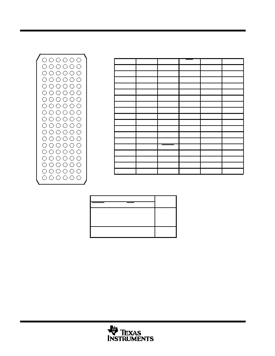
terminal assignments
1
2
3
4
5
6
A
Q2A
Q1A
CLK
CLK
Q1B
Q2B
B
Q3A
VDDQ
GND
GND
VDDQ
Q3B
C
Q5A
Q4A
VDDQ
VDDQ
Q4B
Q5B
D
Q7A
Q6A
GND
GND
Q6B
Q7B
E
Q8A
GND
VDDQ
VDDQ
GND
Q8B
F
Q10A
Q9A
VDDQ
VDDQ
Q9B
Q10B
G
Q12A
Q11A
GND
GND
Q11B
Q12B
H
Q13A
VCC
VDDQ
VDDQ
VCC
Q13B
J
Q14A
Q15A
GND
GND
Q15B
Q14B
K
Q17A
Q16A
VDDQ
VDDQ
Q16B
Q17B
L
Q18A
Q19A
GND
GND
Q19B
Q18B
M
Q20A
VDDQ
GND
GND
VDDQ
Q20B
N
Q22A
Q21A
VDDQ
VDDQ
Q21B
Q22B
P
Q23A
VDDQ
GND
GND
VDDQ
Q23B
R
Q24A
VCC
RESET
VREF
VCC
Q24B
T
D2
D1
D6
D18
D13
D14
U
D4
D3
D10
D22
D15
D16
V
D5
D7
D11
D23
D19
D17
W
D8
D9
D12
D24
D21
D20
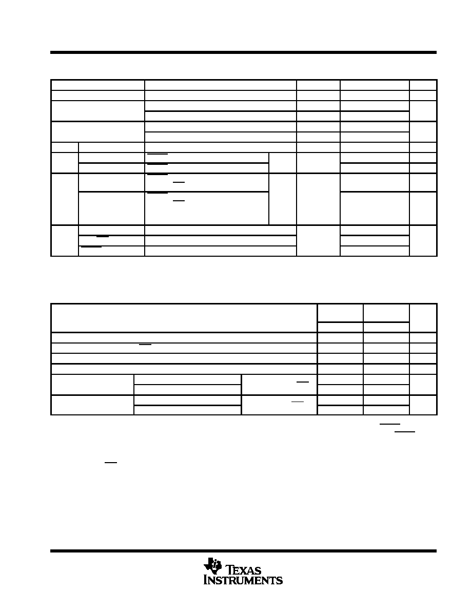
FUNCTION TABLE
INPUTS
OUTPUT
RESET
CLK
CLK
D
Q
H
H
H
H
L
L
H
L or H
L or H
X
Q0
L
X or
floating
X or
floating
X or
floating
L
GKF PACKAGE
(TOP VIEW)
J
H
G
F
E
D
C
B
A
2
1
3
4
6
5
P
N
M
L
K
T
R
U
W
V
SN74SSTVF32852
24-BIT TO 48-BIT REGISTERED BUFFER
WITH SSTL_2 INPUTS AND OUTPUTS
SCES426A ≠ FEBRUARY 2003 ≠ REVISED MARCH 2003
3
POST OFFICE BOX 655303
∑
DALLAS, TEXAS 75265
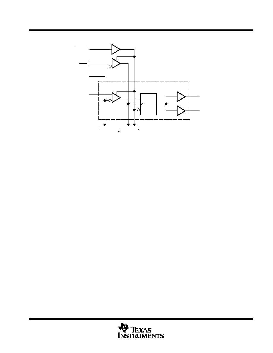
logic diagram (positive logic)
1D
C1
R
To 23 Other Channels
R3
A2
RESET
Q1A
A4
CLK
A3
CLK
R4
VREF
T2
D1
A5
Q1B
One of 24 Channels
absolute maximum ratings over operating free-air temperature range (unless otherwise noted)
Supply voltage range, V
CC
or V
DDQ
≠0.5 V to 3.6 V
. . . . . . . . . . . . . . . . . . . . . . . . . . . . . . . . . . . . . . . . . . . . . . . . .
Input voltage range, V
I
(see Notes 1 and 2)
≠0.5 V to V
CC
+ 0.5 V
. . . . . . . . . . . . . . . . . . . . . . . . . . . . . . . . . . . .
Output voltage range, V
O
(see Notes 1 and 2)
≠0.5 V to V
DDQ
+ 0.5 V
. . . . . . . . . . . . . . . . . . . . . . . . . . . . . . . .
Input clamp current, I
IK
(V
I
< 0)
≠50 mA
. . . . . . . . . . . . . . . . . . . . . . . . . . . . . . . . . . . . . . . . . . . . . . . . . . . . . . . . . . .
Output clamp current, I
OK
(V
O
< 0 or V
O
> V
DDQ
)
±
50 mA
. . . . . . . . . . . . . . . . . . . . . . . . . . . . . . . . . . . . . . . . . .
Continuous output current, I
O
(V
O
= 0 to V
DDQ
)
±
50 mA
. . . . . . . . . . . . . . . . . . . . . . . . . . . . . . . . . . . . . . . . . . . .
Continuous current through each V
CC
, V
DDQ
, or GND
±
100 mA
. . . . . . . . . . . . . . . . . . . . . . . . . . . . . . . . . . . . . .
Package thermal impedance,
q
JA
(see Note 3)
36
∞
C/W
. . . . . . . . . . . . . . . . . . . . . . . . . . . . . . . . . . . . . . . . . . . . .
Storage temperature range, T
stg
≠65
∞
C to 150
∞
C
. . . . . . . . . . . . . . . . . . . . . . . . . . . . . . . . . . . . . . . . . . . . . . . . . . .
Stresses beyond those listed under "absolute maximum ratings" may cause permanent damage to the device. These are stress ratings only, and
functional operation of the device at these or any other conditions beyond those indicated under "recommended operating conditions" is not
implied. Exposure to absolute-maximum-rated conditions for extended periods may affect device reliability.
NOTES:
1. The input and output negative-voltage ratings may be exceeded if the input and output clamp-current ratings are observed.
2. This value is limited to 3.6 V maximum.
3. The package thermal impedance is calculated in accordance with JESD 51-7.
SN74SSTVF32852
24-BIT TO 48-BIT REGISTERED BUFFER
WITH SSTL_2 INPUTS AND OUTPUTS
SCES426A ≠ FEBRUARY 2003 ≠ REVISED MARCH 2003
4
POST OFFICE BOX 655303
∑
DALLAS, TEXAS 75265
recommended operating conditions (see Note 4)
MIN
NOM
MAX
UNIT
VCC
Supply voltage
VDDQ
2.7
V
VDDQ
Output supply voltage
PC1600, PC2100, PC2700
2.3
2.7
V
VDDQ
Output supply voltage
PC3200
2.5
2.7
V
VREF
Reference voltage (VREF = VDDQ/2)
PC1600, PC2100, PC2700
1.15
1.25
1.35
V
VREF
Reference voltage (VREF = VDDQ/2)
PC3200
1.25
1.3
1.35
V
VTT
Termination voltage
VREF≠40mV
VREF
VREF+40mV
V
VI
Input voltage
0
VCC
V
VIH
AC high-level input voltage
Data inputs
VREF+310mV
V
VIL
AC low-level input voltage
Data inputs
VREF≠310mV
V
VIH
DC high-level input voltage
Data inputs
VREF+150mV
V
VIL
DC low-level input voltage
Data inputs
VREF≠150mV
V
VIH
High-level input voltage
RESET
1.7
V
VIL
Low-level input voltage
RESET
0.7
V
VICR
Common-mode input voltage range
CLK, CLK
0.97
1.53
V
VI(PP) Peak-to-peak input voltage
CLK, CLK
360
mV
IOH
High-level output current
≠8
mA
IOL
Low-level output current
8
mA
TA
Operating free-air temperature
0
70
_
C
NOTE 4: The RESET input of the device must be held at valid logic voltage levels (not floating) to ensure proper device operation. The differential
inputs must not be floating unless RESET is low. Refer to the TI application report, Implications of Slow or Floating CMOS Inputs,
literature number SCBA004.
electrical characteristics for PC1600, PC2100, and PC2700 over recommended operating free-air
temperature range (unless otherwise noted)
PARAMETER
TEST CONDITIONS
VCC
MIN
TYP
MAX
UNIT
VIK
II = ≠18 mA
2.3 V
≠1.2
V
VOH
IOH = ≠100
µ
A
2.3 V to 2.7 V
VDDQ≠0.2
V
VOH
IOH = ≠8 mA
2.3 V
1.95
V
VOL
IOL = 100
µ
A
2.3 V to 2.7 V
0.2
V
VOL
IOL = 8 mA
2.3 V
0.35
V
II
All inputs
VI = VCC or GND
2.7 V
±
5
µ
A
ICC
Static standby
RESET = GND
IO = 0
2 7 V
10
µ
A
ICC
Static operating
RESET = VCC, VI = VIH(AC) or VIL(AC)
IO = 0
2.7 V
35
mA
Dynamic operating ≠
clock only
RESET = VCC, VI = VIH(AC) or VIL(AC),
CLK and CLK switching 50% duty cycle
38
µ
A/
MHz
ICCD
Dynamic operating ≠
per each data input
RESET = VCC, VI = VIH(AC) or VIL(AC),
CLK and CLK switching 50% duty cycle,
One data input switching at one-half
clock frequency, 50% duty cycle
IO = 0
2.5 V
7
µ
A/
clock
MHz/
D input
Data inputs
VI = VREF
±
310 mV
2.8
3.3
3.8
Ci
CLK, CLK
VICR = 1.25 V, VI(PP) = 360mV
2.5 V
2.5
3
3.5
pF
RESET
VI = VCC or GND
3
4
4.5
For this test condition, VDDQ always is equal to VCC.
All typical values are at VCC = 2.5 V, TA = 25
∞
C.
SN74SSTVF32852
24-BIT TO 48-BIT REGISTERED BUFFER
WITH SSTL_2 INPUTS AND OUTPUTS
SCES426A ≠ FEBRUARY 2003 ≠ REVISED MARCH 2003
5
POST OFFICE BOX 655303
∑
DALLAS, TEXAS 75265
electrical characteristics for PC3200 over recommended operating free-air temperature range
(unless otherwise noted)
PARAMETER
TEST CONDITIONS
VCC
MIN
TYP
MAX
UNIT
VIK
II = ≠18 mA
2.5 V
≠1.2
V
VOH
IOH = ≠100
µ
A
2.5 V to 2.7 V
VDDQ≠0.2
V
VOH
IOH = ≠8 mA
2.5 V
1.95
V
VOL
IOL = 100
µ
A
2.5 V to 2.7 V
0.2
V
VOL
IOL = 8 mA
2.5 V
0.35
V
II
All inputs
VI = VCC or GND
2.7 V
±
5
µ
A
ICC
Static standby
RESET = GND
IO = 0
2 7 V
10
µ
A
ICC
Static operating
RESET = VCC, VI = VIH(AC) or VIL(AC)
IO = 0
2.7 V
35
mA
Dynamic operating ≠
clock only
RESET = VCC, VI = VIH(AC) or VIL(AC),
CLK and CLK switching 50% duty cycle
38
µ
A/
MHz
ICCD
Dynamic operating ≠
per each data input
RESET = VCC, VI = VIH(AC) or VIL(AC),
CLK and CLK switching 50% duty cycle,
One data input switching at one-half
clock frequency, 50% duty cycle
IO = 0
2.6 V
7
µ
A/
clock
MHz/
D input
Data inputs
VI = VREF
±
310 mV
2.8
3.3
3.8
Ci
CLK, CLK
VICR = 1.25 V, VI(PP) = 360mV
2.6 V
2.5
3
3.5
pF
RESET
VI = VCC or GND
3
4
4.5
For this test condition, VDDQ always is equal to VCC.
All typical values are at VCC = 2.6 V, TA = 25
∞
C.
timing requirements over recommended operating free-air temperature range (unless otherwise
noted) (see Figure 1)
VCC = 2.5 V
±
0.2 V
VCC = 2.6 V
±
0.1 V
UNIT
MIN
MAX
MIN
MAX
fclock
Clock frequency
500
500
MHz
tw
Pulse duration, CLK, CLK high or low
1
1
ns
tact
Differential inputs active time (see Note 5)
22
22
ns
tinact
Differential inputs inactive time (see Note 6)
22
22
ns
t
Setup time
Fast slew rate (see Notes 7 and 9)
D t b f
CLK
CLK
0.75
0.75
ns
tsu
Setup time
Slow slew rate (see Notes 8 and 9)
Data before CLK
, CLK
0.9
0.9
ns
th
Hold time
Fast slew rate (see Notes 7 and 9)
Data after CLK
CLK
0.75
0.75
ns
th
Hold time
Slow slew rate (see Notes 8 and 9)
Data after CLK
, CLK
0.9
0.9
ns
For this test condition, VDDQ always is equal to VCC.
NOTES:
5. VREF must be held at a valid input level and data inputs must be held low for a minimum time of tact max, after RESET is taken high.
6. VREF, data, and clock inputs must be held at valid voltage levels (not floating) for a minimum time of tinact max, after RESET is taken
low.
7. For data signal input slew rate
1 V/ns.
8. For data signal input slew rate
0.5 V/ns and
<
1 V/ns.
9. CLK, CLK signals input slew rates are
1 V/ns.