SN74TVC3010
10-BIT VOLTAGE CLAMP
SCDS088G ≠ APRIL 1999 ≠ REVISED AUGUST 2003
1
POST OFFICE BOX 655303
∑
DALLAS, TEXAS 75265
D
Designed to be Used in Voltage-Limiting
Applications
D
6.5-
On-State Connection Between Ports
A and B
D
Flow-Through Pinout for Ease of Printed
Circuit Board Trace Routing
D
Direct Interface With GTL+ Levels
D
ESD Protection Exceeds JESD 22
≠ 2000-V Human-Body Model (A114-A)
≠ 1000-V Charged-Device Model (C101)
description/ordering information
The SN74TVC3010 provides 11 parallel NMOS
pass transistors with a common gate. The low
on-state resistance of the switch allows
connections to be made with minimal propagation
delay.
The device can be used as a 10-bit switch with the gates cascaded together to a reference transistor. The
low-voltage side of each pass transistor is limited to a voltage set by the reference transistor. This is done to
protect components with inputs that are sensitive to high-state voltage-level overshoots. (See Application
Information in this data sheet.)
All of the transistors in the TVC array have the same electrical characteristics; therefore, any one of them can
be used as the reference transistor. Since, within the device, the characteristics from transistor to transistor are
equal, the maximum output high-state voltage (V
OH
) is approximately the reference voltage (V
REF
), with
minimal deviation from one output to another. This is a large benefit of the TVC solution over discrete devices.
Because the fabrication of the transistors is symmetrical, either port connection of each bit can be used as the
low-voltage side, and the I/O signals are bidirectional through each FET.
ORDERING INFORMATION
TA
PACKAGE
ORDERABLE
PART NUMBER
TOP-SIDE
MARKING
≠40 C to 85 C
SOIC ≠ DW
Tube
SN74TVC3010DW
TVC3010
≠40 C to 85 C
SOIC ≠ DW
Tape and reel
SN74TVC3010DWR
TVC3010
≠40
∞
C to 85
∞
C
SSOP (QSOP) ≠ DBQ
Tape and reel
SN74TVC3010DBQR
TVC3010
TSSOP ≠ PW
Tape and reel
SN74TVC3010PWR
TT010
TVSOP ≠ DGV
Tape and reel
SN74TVC3010DGVR
TT010
Package drawings, standard packing quantities, thermal data, symbolization, and PCB design
guidelines are available at www.ti.com/sc/package.
Copyright
2003, Texas Instruments Incorporated
Please be aware that an important notice concerning availability, standard warranty, and use in critical applications of
Texas Instruments semiconductor products and disclaimers thereto appears at the end of this data sheet.
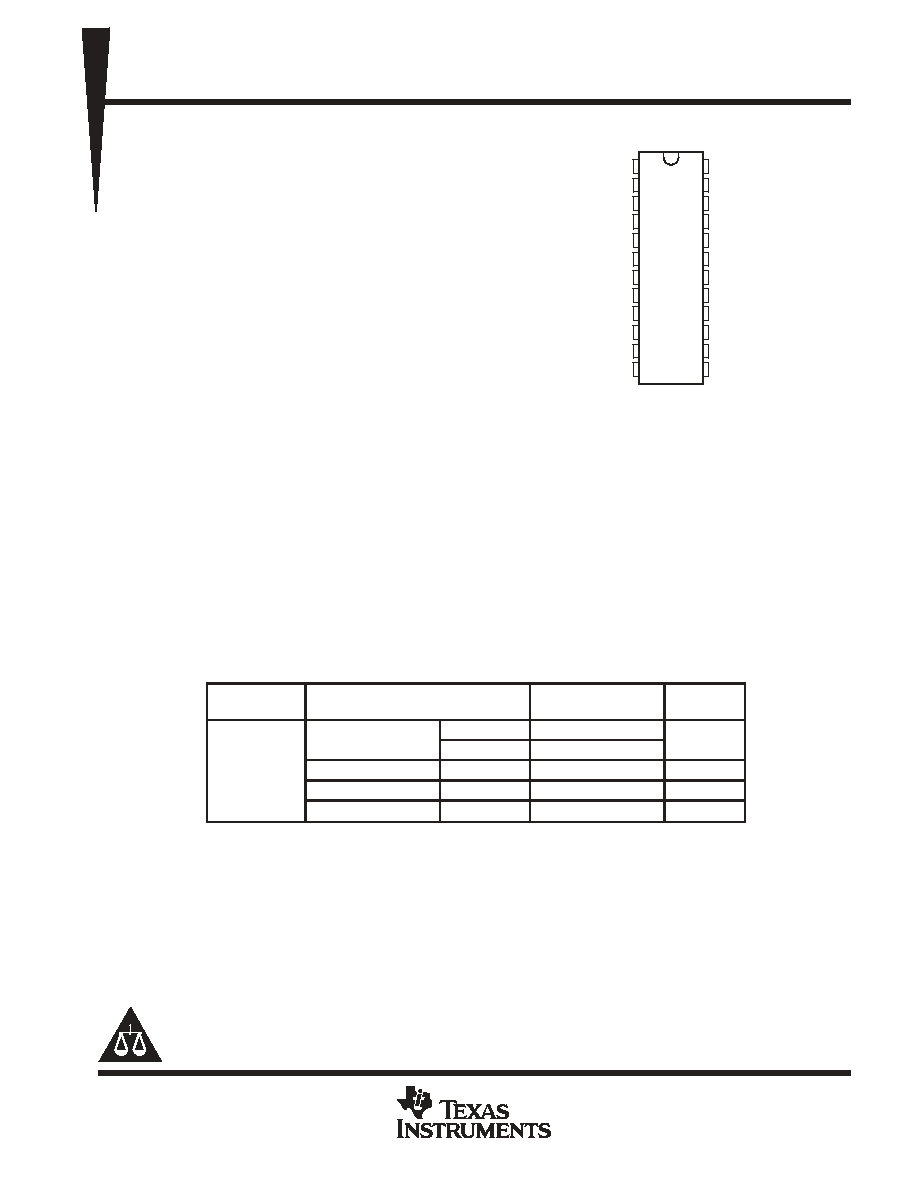
DBQ, DGV, DW, OR PW PACKAGE
(TOP VIEW)
1
2
3
4
5
6
7
8
9
10
11
12
24
23
22
21
20
19
18
17
16
15
14
13
GND
A1
A2
A3
A4
A5
A6
A7
A8
A9
A10
A11
GATE
B1
B2
B3
B4
B5
B6
B7
B8
B9
B10
B11
PRODUCTION DATA information is current as of publication date.
Products conform to specifications per the terms of Texas Instruments
standard warranty. Production processing does not necessarily include
testing of all parameters.
SN74TVC3010
10-BIT VOLTAGE CLAMP
SCDS088G ≠ APRIL 1999 ≠ REVISED AUGUST 2003
2
POST OFFICE BOX 655303
∑
DALLAS, TEXAS 75265
simplified schematic
24
23
22
21
20
13
1
2
3
4
5
12
GND
A1
A2
A3
A4
A11
GATE
B1
B2
B3
B4
B11
absolute maximum ratings over operating free-air temperature range (unless otherwise noted)
Input voltage range, V
I
(see Note 1)
≠0.5 V to 7 V
. . . . . . . . . . . . . . . . . . . . . . . . . . . . . . . . . . . . . . . . . . . . . . . . . .
Input/output voltage range, V
I/O
(see Note 1)
≠0.5 V to 7 V
. . . . . . . . . . . . . . . . . . . . . . . . . . . . . . . . . . . . . . . . . .
Continuous channel current
128 mA
. . . . . . . . . . . . . . . . . . . . . . . . . . . . . . . . . . . . . . . . . . . . . . . . . . . . . . . . . . . . . .
Input clamp current, I
IK
(V
I
< 0)
≠50 mA
. . . . . . . . . . . . . . . . . . . . . . . . . . . . . . . . . . . . . . . . . . . . . . . . . . . . . . . . . . .
Package thermal impedance,
JA
(see Note 2): DBQ package
61
∞
C/W
. . . . . . . . . . . . . . . . . . . . . . . . . . . . . . . .
DGV package
86
∞
C/W
. . . . . . . . . . . . . . . . . . . . . . . . . . . . . . . .
DW package
46
∞
C/W
. . . . . . . . . . . . . . . . . . . . . . . . . . . . . . . . .
PW package
88
∞
C/W
. . . . . . . . . . . . . . . . . . . . . . . . . . . . . . . . .
Storage temperature range, T
stg
≠65
∞
C to 150
∞
C
. . . . . . . . . . . . . . . . . . . . . . . . . . . . . . . . . . . . . . . . . . . . . . . . . . .
Stresses beyond those listed under "absolute maximum ratings" may cause permanent damage to the device. These are stress ratings only, and
functional operation of the device at these or any other conditions beyond those indicated under "recommended operating conditions" is not
implied. Exposure to absolute-maximum-rated conditions for extended periods may affect device reliability.
NOTES:
1. The input and input/output negative-voltage ratings may be exceeded if the input and input/output clamp-current ratings are
observed.
2. The package thermal impedance is calculated in accordance with JESD 51-7.
recommended operating conditions
MIN
TYP
MAX
UNIT
VI/O
Input/output voltage
0
5
V
VGATE
GATE voltage
0
5
V
IPASS
Pass-transistor current
20
64
mA
TA
Operating free-air temperature
≠40
85
∞
C
SN74TVC3010
10-BIT VOLTAGE CLAMP
SCDS088G ≠ APRIL 1999 ≠ REVISED AUGUST 2003
3
POST OFFICE BOX 655303
∑
DALLAS, TEXAS 75265
application operating conditions (see Figure 3)
MIN
TYP
MAX
UNIT
VBIAS
BIAS voltage
VREF + 0.6
2.1
5
V
VGATE
GATE voltage
VREF + 0.6
2.1
5
V
VREF
Reference voltage
0
1.5
4.4
V
VDPU
Drain pullup voltage
2.36
2.5
2.64
V
IPASS
Pass-transistor current
14
mA
IREF
Reference-transistor current
5
µ
A
TA
Operating free-air temperature
≠40
85
∞
C
electrical characteristics over recommended operating free-air temperature range (unless
otherwise noted)
PARAMETER
TEST CONDITIONS
MIN
TYP
MAX
UNIT
VIK
VBIAS = 0,
II = ≠18 mA
≠1.2
V
VOL
IREF = 5
m
A,
VDPU = 2.625 V,
VREF = 1.365 V,
RDPU = 150
VS = 0.175 V,
See Figure 1
350
mV
Ci(GATE)
VI = 3 V or 0
24
pF
Cio(off)
VO = 3 V or 0
4
12
pF
Cio(on)
VO = 3 V or 0
12
30
pF
ron
IREF = 5
m
A,
VDPU = 2.625 V,
VREF = 1.365 V,
RDPU = 150
VS = 0.175 V,
See Figure 1
12.5
All typical values are at TA = 25
∞
C.
Measured by the voltage drop between the A and B terminals at the indicated current through the switch. On-state resistance is determined by
the lowest voltage of the two (A or B) terminals.
switching characteristics over recommended operating free-air temperature range,
V
DPU
= 2.36 V to 2.64 V (unless otherwise noted) (see Figure 1)
PARAMETER
FROM
(INPUT)
TO
(OUTPUT)
MIN
MAX
UNIT
tPLH
A or B
B or A
0
4
ns
tPHL
A or B
B or A
0
4
ns
SN74TVC3010
10-BIT VOLTAGE CLAMP
SCDS088G ≠ APRIL 1999 ≠ REVISED AUGUST 2003
4
POST OFFICE BOX 655303
∑
DALLAS, TEXAS 75265
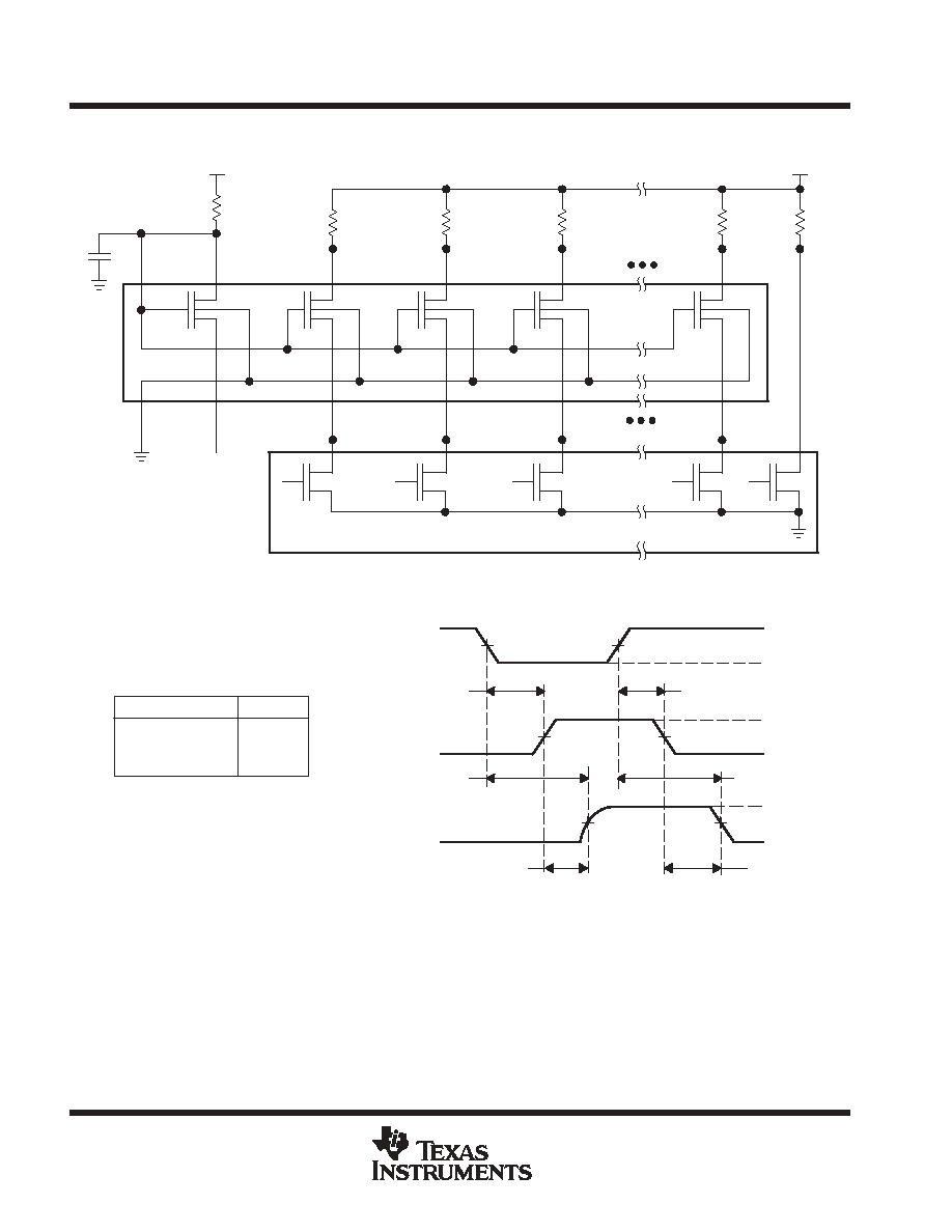
PARAMETER MEASUREMENT INFORMATION
tPLHREF
tPHLREF
2.5 V
0 V
2.5 V
VOL
Input
Tester
VOLTAGE WAVEFORMS
PROPAGATION DELAY TIMES
Output
Reference
TESTER CALIBRATION SETUP (see Note C)
VOL
Output
Device
Under Test
tPLHDUT
tPLH
(see Note D)
tPHLDUT
tPHL
(see Note E)
2.5 V
200 k
3.3 V
RDPU =
150
Open-Drain
Test Interface
Motherboard
Interface
2
A1 (VREF)
1
GATE
24
B1 (VBIAS)
23
VDPU
TVC3010
NOTES: A. All input pulses are supplied by generators having the following characteristics: PRR
10 MHz, ZO = 50
, tr
2 ns, tf
2 ns.
B. The outputs are measured one at a time with one transition per measurement.
C. Test procedure: tPLHREF and tPHLREF are obtained by measuring the propagation delay of a reference measuring point.
tPLHDUT and tPHLDUT are obtained by measuring the propagation delay of the device under test.
D. tPLH = tPLHDUT ≠ tPLHREF
E. tPHL = tPHLDUT ≠ tPHLREF
B2
22
RDPU =
150
RDPU =
150
RDPU =
150
B3
21
B4
20
B11
13
3
A2 (VS)
4
A3 (VS)
5
A4 (VS)
12
A11 (VS)
1.25 V
1.25 V
1.25 V
1.25 V
1.25 V
1.25 V
ß
ß
ß
ß
Output tested
Output reference
Input tested
ß
DEFINITION
SYMBOL
GATE
Figure 1. Tester Calibration Setup and Voltage Waveforms
SN74TVC3010
10-BIT VOLTAGE CLAMP
SCDS088G ≠ APRIL 1999 ≠ REVISED AUGUST 2003
5
POST OFFICE BOX 655303
∑
DALLAS, TEXAS 75265
APPLICATION INFORMATION
TVC background information
In personal computer (PC) architecture, there are industry-accepted bus standards. These standards define,
among other things, the I/O voltage levels at which the bus communicates. Examples include the GTL+ host
bus, the AGP graphics port, and the PCI local bus. In new designs, the system components must communicate
with existing bus infrastructure. Providing an evolutionary upgrade path is important in the design of PC
architecture, but the existing bus standards must be preserved.
To achieve the ever-present need for smaller, faster, lighter devices that draw less power, yet have faster
performance, most new high-performance digital integrated circuits are being designed and produced with
advanced submicron semiconductor process technologies. These devices have thin gate-oxide or short
channel lengths and very low absolute-maximum voltages that can be tolerated at the inputs/outputs (I/Os)
without causing damage. In many cases, the I/Os of these devices are not tolerant of the high-state voltage
levels on the preexisting buses with which they must communicate. Therefore, it became necessary to protect
the I/Os of devices by limiting the I/O voltages.
The Texas Instruments (TI) translation voltage-clamp (TVC) family was designed specifically for protecting
sensitive I/Os (see Figure 2). The information in this data sheet describes the I/O-protection application of the
TVC family and should enable the design engineer to successfully implement an I/O-protection circuit utilizing
the TI TVC solution.
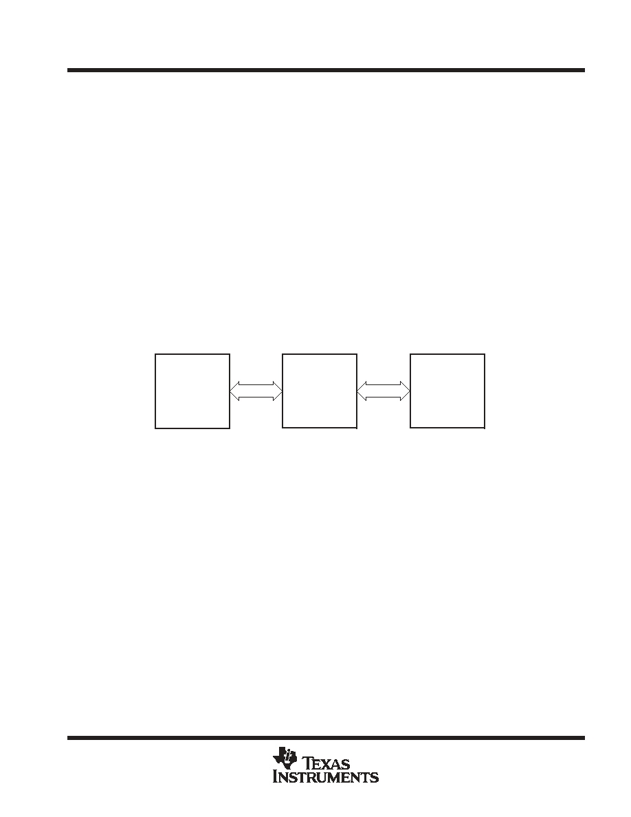
Low-Voltage
I/O Device
TVC Family
Voltage-Clamp
Device
Standard-Voltage
I/O Bus
Figure 2. Thin Gate-Oxide Protection Application