SN55116, SN75116, SN75117, SN75118, SN75119
DIFFERENTIAL LINE TRANSCEIVERS
SLLS073D ≠ MAY 1976 ≠ REVISED MAY 1998
1
POST OFFICE BOX 655303
∑
DALLAS, TEXAS 75265
features common to all types
D
Single 5-V Supply
D
3-State Driver Output Circuitry
D
TTL-Compatible Driver Inputs
D
TTL-Compatible Receiver Output
D
Differential Line Operation
D
Receiver Output Strobe (SN55116,
SN75116, SN75117) or Enable (SN75118,
SN75119)
D
Designed for Party-Line (Data-Bus)
Applications
additional features of the SN55116/SN75116
D
Choice of Ceramic or Plastic Packages
D
Independent Driver and Receiver
D
Choice of Open-Collector or Totem-Pole
Outputs on Both Driver and Receiver
D
Dual Data Inputs on Driver
D
Optional Line-Termination Resistor in
Receiver
D
±
15-V Receiver Common-Mode Capability
D
Receiver Frequency-Response Control
additional features of the SN75117
D
Driver Output Internally Connected to
Receiver Input
The SN75118 is an SN75116 With 3-State Receiver Output Circuitry
The SN75119 is an SN75117 With 3-State Receiver Output Circuitry
description
These integrated circuits are designed for use in interfacing between TTL-type digital systems and differential
data-transmission lines. They are especially useful for party-line (data-bus) applications. Each of these circuit
types combine in one package a 3-state differential line driver and a differential-input line receiver, both of which
operate from a single 5-V power supply. The driver inputs and the receiver outputs are TTL compatible. The
driver employed is similar to the SN55113 and SN75113 3-state line drivers, and the receiver is similar to the
SN55115 and SN75115 line receivers.
The SN55116, SN75116, and SN75118 offer all the features of the SN55113 and SN75113 drivers and the
SN55115 and SN75115 receivers combined. The driver performs the dual input AND and NAND functions when
enabled or presents a high impedance to the load when in the disabled state. The driver output stages are similar
to TTL totem-pole outputs, but have the current-sinking portion separated from the current-sourcing portion and
both are brought out to adjacent package terminals. This feature allows the user the option of using the driver
in the open-collector output configuration, or, by connecting the adjacent source and sink terminals together,
of using the driver in the normal totem-pole output configuration.
The receiver portion of the SN55116, SN75116, and SN75118 features a differential-input circuit having a
common-mode voltage range of
±
15 V. An internal 130-
equivalent resistor also is provided, which optionally
can be used to terminate the transmission line. A frequency-response control terminal allows the user to reduce
the speed of the receiver or to improve differential noise immunity. The receivers of the SN55116 and SN75116
have an output strobe and a split totem-pole output. The receiver of the SN75118 has an output-enable for the
3-state split totem-pole output. The receiver section of either circuit is independent of the driver section except
for the V
CC
and ground terminals.
The SN75117 and SN75119 provide the basic driver and receiver functions of the SN55116, SN75116, and
SN75118, but use a package that is only half as large. The SN75117 and SN75119 are intended primarily for
party-line or bus-organized systems because the driver outputs are internally connected to the receiver inputs.
The driver has a single data input and a single enable input. The SN75117 receiver has an output strobe, while
the SN75119 receiver has a 3-state output enable. However, these devices do not provide output connection
options, line-termination resistors, or receiver frequency-response controls.
Copyright
©
1998, Texas Instruments Incorporated
PRODUCTION DATA information is current as of publication date.
Products conform to specifications per the terms of Texas Instruments
standard warranty. Production processing does not necessarily include
testing of all parameters.
Please be aware that an important notice concerning availability, standard warranty, and use in critical applications of
Texas Instruments semiconductor products and disclaimers thereto appears at the end of this data sheet.
SN55116, SN75116, SN75117, SN75118, SN75119
DIFFERENTIAL LINE TRANSCEIVERS
SLLS073D ≠ MAY 1976 ≠ REVISED MAY 1998
2
POST OFFICE BOX 655303
∑
DALLAS, TEXAS 75265
description (continued)
The SN55116 is characterized for operation over the full military temperature range of ≠ 55
∞
C to 125
∞
C. The
SN75116, SN75117, SN75118, and SN75119 are characterized for operation from 0
∞
C to 70
∞
C.
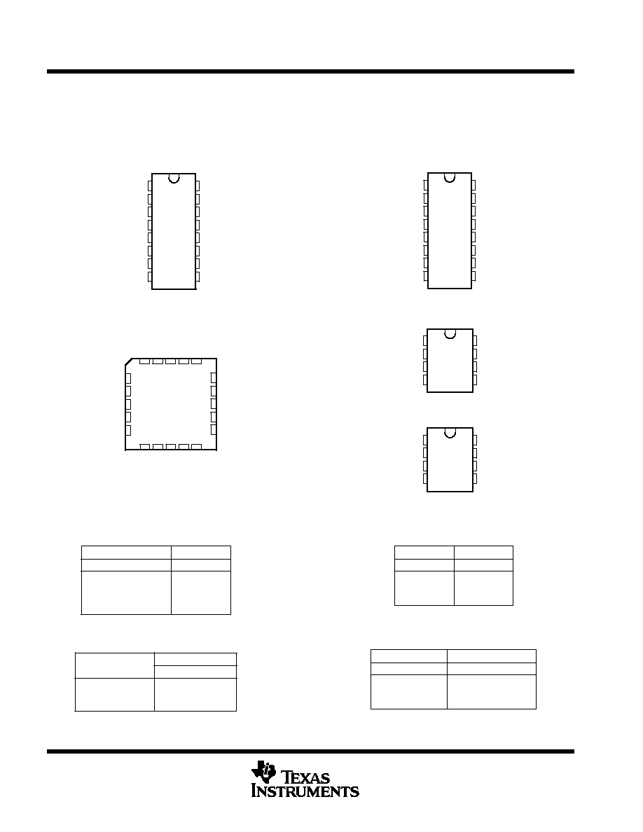
1
2
3
4
5
6
7
8
16
15
14
13
12
11
10
9
DZP
DZS
DYS
DYP
RA
R
T
RB
GND
V
CC
DB
DA
DE
RYP
RYS
RS
RTC
SN55116 . . . J PACKAGE
SN75116 . . . D OR N PACKAGE
(TOP VIEW)
1
2
3
4
5
6
7
8
16
15
14
13
12
11
10
9
DZP
DZS
DYS
DYP
RA
R
T
RB
GND
V
CC
DB
DA
DE
RYP
RYS
RE
RTC
SN75118 . . . D OR N PACKAGE
(TOP VIEW)
3
2
1 20 19
9 10 11 12 13
4
5
6
7
8
18
17
16
15
14
DA
DE
NC
RYP
RYS
DYS
DYP
NC
RA
R
T
SN55116 . . . FK PACKAGE
(TOP VIEW)
DZS
DZP
NC
RS
DB
RB
GND
NC
NC ≠ No internal connection
CC
V
RT
C
1
2
3
4
8
7
6
5
DI
B
A
GND
V
CC
DE
RY
RS
SN75117 . . . D OR P PACKAGE
(TOP VIEW)
1
2
3
4
8
7
6
5
DI
B
A
GND
V
CC
DE
RY
RE
SN75119 . . . D OR P PACKAGE
(TOP VIEW)
Function Tables
INPUTS
OUTPUTS
L
H
H
H
'116, SN75118
DRIVER
DE
DA
DB
X
L
X
H
X
X
L
H
DY
DZ
Z
L
L
H
Z
H
H
L
INPUTS
OUTPUTS
SN75117, SN75119
DRIVER
DI
DE
H
L
X
H
H
L
A
B
H
L
Z
L
H
Z
OUTPUTS RY
'116, SN75118
RECEIVER
RS/RE
DIFF
INPUT
L
H
H
X
L
H
'116
SN75118
H
H
L
Z
H
L
INPUTS
OUTPUT RY
SN75117, SN75119
RECEIVER
B
RS/RE
L
H
X
H
H
L
SN75117
SN75119
H
L
H
H
L
Z
A
H
L
X
H = high level (VI
VIH min or VID more positive than VTH max), L = low level (VI
VIL max or VID more negative than VTL max),
X = irrelevant, Z = high impedance (off)
SN55116, SN75116, SN75117, SN75118, SN75119
DIFFERENTIAL LINE TRANSCEIVERS
SLLS073D ≠ MAY 1976 ≠ REVISED MAY 1998
3
POST OFFICE BOX 655303
∑
DALLAS, TEXAS 75265
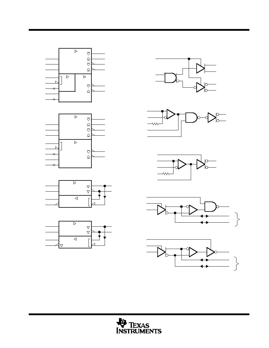
logic symbol
EN
B
A
6
5
1
7
RY
RS
DI
DE
2
3
&
&
&
RESP
RT
EN
9
10
6
5
7
15
14
13
RYS
RYP
DZS
DZP
DYS
DYP
RTC
RS
RT
RA
RB
DB
DA
DE
11
12
2
1
3
4
'116
&
RESP
RT
EN
9
10
6
5
7
15
14
13
RYS
RYP
DZS
DZP
DYS
DYP
RTC
RE
RT
RA
RB
DB
DA
DE
11
12
2
1
3
4
SN75118
EN
SN75117
EN
B
A
6
5
1
7
RY
RE
DI
DE
2
3
SN75119
EN
5
logic diagram (positive logic)
6
3
2
5
7
1
RE
DE
DI
RY
A
B
BUS
BUS
B
A
RY
DI
DE
RS
1
7
5
2
3
6
RTC
RT
RA
RB
RE
9
6
5
7
10
RYP (pullup)
RYS (sink)
12
11
RS
RTC
RT
RA
RB
10
9
6
7
RYS (sink)
RYP (pullup)
11
12
DB
DA
DE
15
14
13
DZS (sink)
DZP (pullup)
DYS (sink)
DYP (pullup)
2
1
3
4
'116 and SN75118
'116 Receiver
SN75118 Receiver
SN75119 Driver and Receiver
SN75117 Driver and Receiver
These symbols are in accordance with ANSI/IEEE Std 91-1984 and IEC Publication 617-12.
Pin numbers shown for the SN55116 and SN75116 are for the D, J, and N packages, those shown for the SN75118 are for the D and N packages,
and those shown for SN75117 and SN75119 are for the D and P packages.
SN55116, SN75116, SN75117, SN75118, SN75119
DIFFERENTIAL LINE TRANSCEIVERS
SLLS073D ≠ MAY 1976 ≠ REVISED MAY 1998
4
POST OFFICE BOX 655303
∑
DALLAS, TEXAS 75265
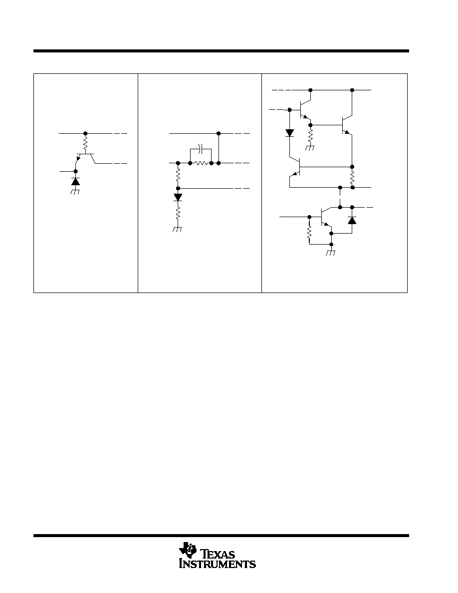
schematics of inputs and outputs
7 k
NOM
EQUIVALENT OF
EACH DRIVER INPUT
AND EACH RE AND RS INPUT
VCC
Input
4 k
NOM
EQUIVALENT OF
EACH RECEIVER INPUT
(EXCLUDING ENABLES AND STROBES)
VCC
1 pF NOM
Input
8 k
NOM
130
NOM
TYPICAL OF ALL OUTPUTS
VCC
R
Pullup
output
Driver output R = 9
NOM
Receiver output R = 20
NOM
Sink
output
On SN75117 and SN75119, common outputs
replace the separate pullup and sink outputs.
absolute maximum ratings over operating free-air temperature (unless otherwise noted)
Supply voltage, V
CC
(see Notes 1 and 2)
7 V
. . . . . . . . . . . . . . . . . . . . . . . . . . . . . . . . . . . . . . . . . . . . . . . . . . . . . .
Input voltage, V
I
: DA, DB, DE, DI, RE, and RS
5.5 V
. . . . . . . . . . . . . . . . . . . . . . . . . . . . . . . . . . . . . . . . . . . . . . . .
RA, RB, R
T
for '116, SN75118 only
±
25 V
. . . . . . . . . . . . . . . . . . . . . . . . . . . . . . . . . . . . . . . . . .
A and B for SN75117, SN75119 only
0 to 6 V
. . . . . . . . . . . . . . . . . . . . . . . . . . . . . . . . . . . . . . .
Off-state voltage applied to open-collector outputs: '116, SN75118 only
12 V
. . . . . . . . . . . . . . . . . . . . . . . . . . .
Continuous total power dissipation (see Note 2)
See Dissipation Rating Table
. . . . . . . . . . . . . . . . . . . . . . . . . .
Storage temperature range, T
stg
≠ 65
∞
C to 150
∞
C
. . . . . . . . . . . . . . . . . . . . . . . . . . . . . . . . . . . . . . . . . . . . . . . . . . .
Case temperature for 60 seconds, T
C
: FK package
260
∞
C
. . . . . . . . . . . . . . . . . . . . . . . . . . . . . . . . . . . . . . . . . .
Lead temperature 1,6 mm (1/16 inch) from case for 60 seconds: J package
300
∞
C
. . . . . . . . . . . . . . . . . . . . .
Lead temperature 1,6 mm (1/16 inch) from case for 10 seconds: D, N, or P package
260
∞
C
. . . . . . . . . . . . .
Stresses beyond those listed under "absolute maximum ratings" may cause permanent damage to the device. These are stress ratings only, and
functional operation of the device at these or any other conditions beyond those indicated under "recommended operating conditions" is not
implied. Exposure to absolute-maximum-rated conditions for extended periods may affect device reliability.
NOTES:
1. All voltage values are with respect to the network ground terminal.
2. In the FK and J packages, the SN55116 chip is alloy mounted. The SN75116, SN75117, SN75118, and SN75119 chips are glass
mounted.
SN55116, SN75116, SN75117, SN75118, SN75119
DIFFERENTIAL LINE TRANSCEIVERS
SLLS073D ≠ MAY 1976 ≠ REVISED MAY 1998
5
POST OFFICE BOX 655303
∑
DALLAS, TEXAS 75265
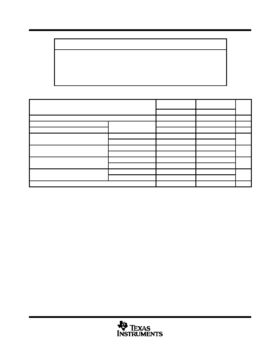
DISSIPATION RATING TABLE
PACKAGE
TA
25
∞
C
POWER RATING
DERATING FACTOR
ABOVE TA = 25
∞
C
TA = 70
∞
C
POWER RATING
TA = 125
∞
C
POWER RATING
D (8 pin)
725 mW
5.8 mW/
∞
C
464 mW
--
D (16 pin)
950 mW
7.6 mW/
∞
C
608 mW
--
FK
1375 mW
11.0 mW/
∞
C
880 mW
275 mW
J
1375 mW
11.0 mW/
∞
C
880 mW
275 mW
N
1150 mW
9.2 mW/
∞
C
736 mW
--
P
1000 mW
8.0 mW/
∞
C
640 mW
--
recommended operating conditions
PARAMETER
SN55116
SN75116, SN75117,
SN75118, SN75119
UNIT
PARAMETER
MIN
NOM
MAX
MIN
NOM
MAX
UNIT
Supply voltage, VCC
4.5
5
5.5
4.5
5
5.5
V
High-level input voltage, VIH
All inputs except differential
2
2
V
Low-level input voltage, VIL
inputs
0.8
0.8
V
High level output current IOH
Drivers
≠ 40
≠ 40
mA
High-level output current, IOH
Receivers
≠ 5
≠ 5
mA
Low level output current IOL
Drivers
40
40
mA
Low-level output current, IOL
Receivers
15
15
mA
Receiver input voltage VI
'116, SN75118
±
15
±
15
V
Receiver input voltage, VI
SN75117, SN75119
0
6
0
6
V
Common mode receiver input voltage VICR
'116, SN75118
±
15
±
15
V
Common-mode receiver input voltage, VICR
SN75117, SN75119
0
6
0
6
V
Operating free-air temperature, TA
≠ 55
125
0
70
∞
C