SN55451B, SN55452B, SN55453B, SN55454B
SN75451B, SN75452B, SN75453B, SN75454B
DUAL PERIPHERAL DRIVERS
SLRS021B ≠ DECEMBER 1976 ≠ REVISED SEPTEMBER 1999
1
POST OFFICE BOX 655303
∑
DALLAS, TEXAS 75265
PERIPHERAL DRIVERS FOR
HIGH-CURRENT SWITCHING AT
VERY HIGH SPEEDS
D
Characterized for Use to 300 mA
D
High-Voltage Outputs
D
No Output Latch-Up at 20 V (After
Conducting 300 mA)
D
High-Speed Switching
D
Circuit Flexibility for Varied Applications
D
TTL-Compatible Diode-Clamped Inputs
D
Standard Supply Voltages
D
Plastic DIP (P) With Copper Lead Frame
Provides Cooler Operation and Improved
Reliability
D
Package Options Include Plastic
Small-Outline Packages, Ceramic Chip
Carriers, and Standard Plastic and Ceramic
300-mil DIPs
SUMMARY OF DEVICES
DEVICE
LOGIC OF
COMPLETE CIRCUIT
PACKAGES
SN55451B
AND
FK, JG
SN55452B
NAND
JG
SN55453B
OR
FK, JG
SN55454B
NOR
JG
SN75451B
AND
D, P
SN75452B
NAND
D, P
SN75453B
OR
D, P
SN75454B
NOR
D, P
description
The SN55451B through SN55454B and SN75451B through SN75454B are dual peripheral drivers designed
for use in systems that employ TTL logic. This family is functionally interchangeable with and replaces the
SN75450 family and the SN75450A family devices manufactured previously. The speed of the devices is equal
to that of the SN75450 family, and the parts are designed to ensure freedom from latch-up. Diode-clamped
inputs simplify circuit design. Typical applications include high-speed logic buffers, power drivers, relay drivers,
lamp drivers, MOS drivers, line drivers, and memory drivers.
The SN55451B/SN75451B, SN55452B/SN75452B, SN55453B/SN75453B, and SN55454B/SN75454B are
dual peripheral AND, NAND, OR, and NOR drivers, respectively (assuming positive logic), with the output of
the logic gates internally connected to the bases of the npn output transistors.
The SN55' drivers are characterized for operation over the full military range of ≠ 55
∞
C to 125
∞
C. The SN75'
drivers are characterized for operation from 0
∞
C to 70
∞
C.
Copyright
©
1999, Texas Instruments Incorporated
PRODUCTION DATA information is current as of publication date.
Products conform to specifications per the terms of Texas Instruments
standard warranty. Production processing does not necessarily include
testing of all parameters.
1
2
3
4
8
7
6
5
1A
1B
1Y
GND
V
CC
2B
2A
2Y
SN55451B, SN55452B,
SN55453B, SN55454B . . . JG PACKAGE
SN75451B, SN75452B,
SN75453B, SN75454B . . . D OR P PACKAGE
(TOP VIEW)
3
2
1 20 19
9 10 11 12 13
4
5
6
7
8
18
17
16
15
14
NC
2B
NC
2A
NC
NC
1B
NC
1Y
NC
SN55451B, SN55452B
SN55453B, SN55454B . . . FK PACKAGE
(TOP VIEW)
NC
1A
NC
NC
NC
NC
GND
NC
NC ≠ No internal connection
CC
V
2Y
SN55451B, SN55452B, SN55453B, SN55454B
SN75451B, SN75452B, SN75453B, SN75454B
DUAL PERIPHERAL DRIVERS
SLRS021B ≠ DECEMBER 1976 ≠ REVISED SEPTEMBER 1999
2
POST OFFICE BOX 655303
∑
DALLAS, TEXAS 75265
absolute maximum ratings over operating free-air temperature range (unless otherwise noted)
SN55'
SN75'
UNIT
Supply voltage, VCC (see Note 1)
7
7
V
Input voltage, VI
5.5
5.5
V
Inter-emitter voltage (see Note 2)
5.5
5.5
V
Off-state output voltage, VO
30
30
V
Continuous collector or output current, IOK (see Note 3)
400
400
mA
Peak collector or output current, II (tw
10 ms, duty cycle
50%, see Note 4)
500
500
mA
Continuous total power dissipation
See Dissipation Rating Table
Operating free-air temperature range, TA
≠ 55 to 125
0 to 70
∞
C
Storage temperature range, Tstg
≠ 65 to 150
≠ 65 to 150
∞
C
Case temperature for 60 seconds
FK package
260
∞
C
Lead temperature 1,6 mm (1/16 inch) from case for 60 seconds
JG package
300
∞
C
Lead temperature 1,6 mm (1/16 inch) from case for 10 seconds
D or P package
260
∞
C
NOTES:
1. Voltage values are with respect to network GND, unless otherwise specified.
2. This is the voltage between two emitters of a multiple-emitter transistor.
3. This value applies when the base-emitter resistance (RBE) is equal to or less than 500
.
4. Both halves of these dual circuits may conduct rated current simultaneously; however, power dissipation averaged over a short time
interval must fall within the continuous dissipation rating.
DISSIPATION RATING TABLE
PACKAGE
TA
25
∞
C
DERATING FACTOR
TA = 70
∞
C
TA = 125
∞
C
PACKAGE
A
POWER RATING
ABOVE TA = 25
∞
C
A
POWER RATING
A
POWER RATING
D
725 mW
5.8 mW/
∞
C
464 mW
--
FK
1375 mW
11.0 mW/
∞
C
880 mW
275 mW
JG
1050 mW
8.4 mW/
∞
C
672 mW
210 mW
P
1000 mW
8.0 mW/
∞
C
640 mW
--
recommended operating conditions
SN55'
SN75'
UNIT
MIN
NOM
MAX
MIN
NOM
MAX
UNIT
Supply voltage, VCC
4.5
5
5.5
4.75
5
5.25
V
High-level input voltage, VIH
2
2
V
Low-level input voltage, VIL
0.8
0.8
V
Operating free-air temperature, TA
≠ 55
125
0
70
∞
C
SN55451B, SN55452B, SN55453B, SN55454B
SN75451B, SN75452B, SN75453B, SN75454B
DUAL PERIPHERAL DRIVERS
SLRS021B ≠ DECEMBER 1976 ≠ REVISED SEPTEMBER 1999
3
POST OFFICE BOX 655303
∑
DALLAS, TEXAS 75265
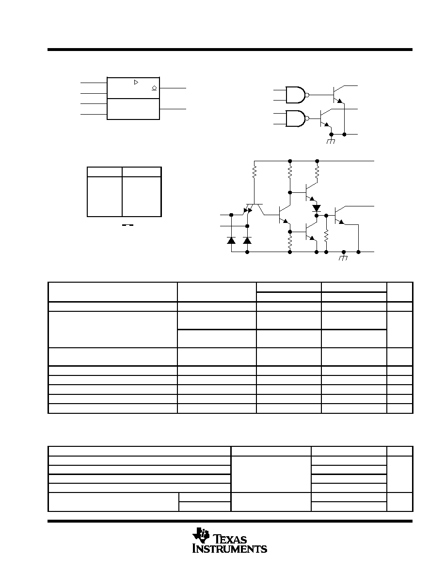
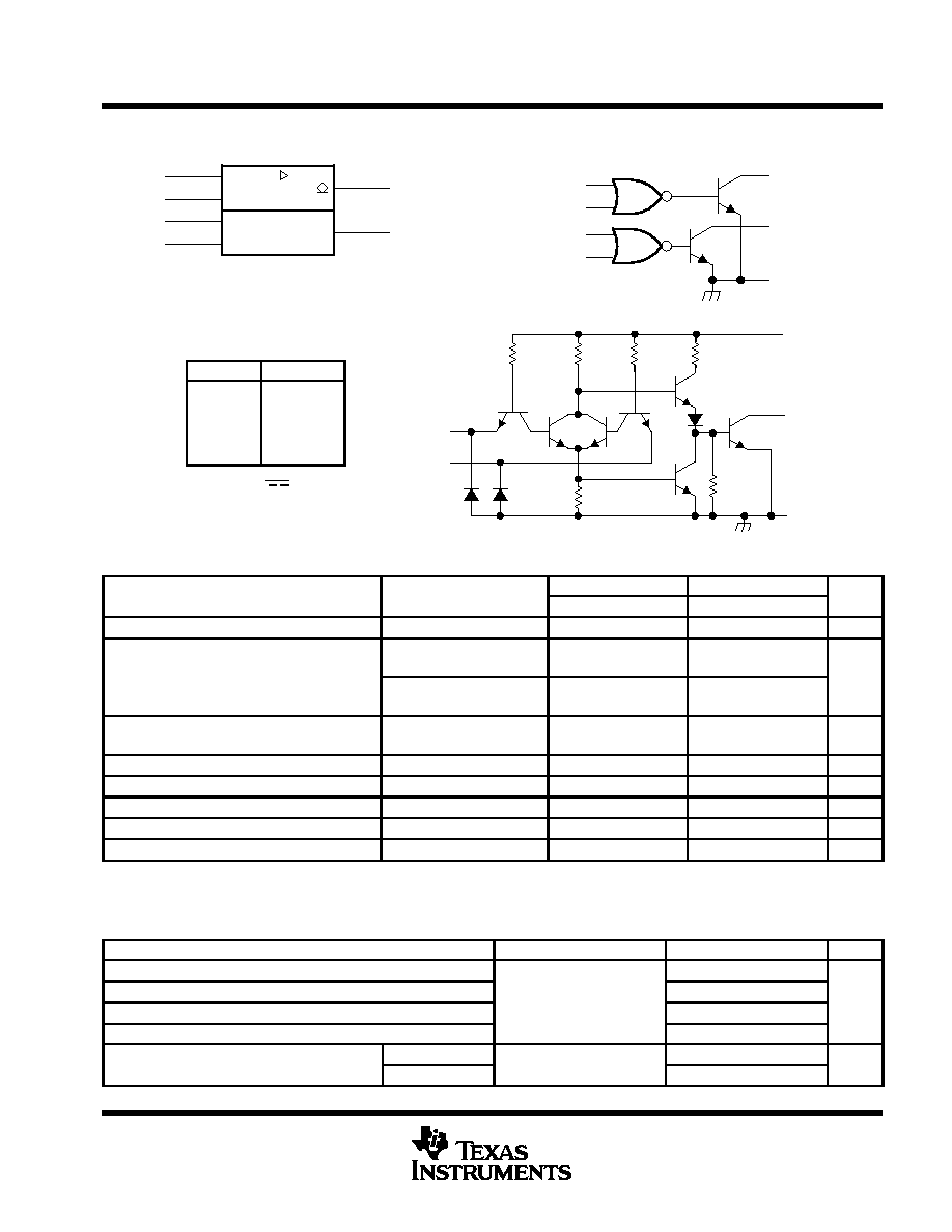
logic symbol
&
5
3
2B
2A
1B
1A
2Y
1Y
7
6
2
1
This symbol is in accordance with ANSI/IEEE Std 91-1984
and IEC publication 617-12.
Pin numbers shown are for the D, JG, and P packages.
logic diagram (positive logic)
2B
2A
1B
1A
4
5
3
GND
2Y
1Y
7
6
2
1
FUNCTION TABLE
(each driver)
A
B
Y
L
L
L (on state)
L
H
L (on state)
H
L
L (on state)
H
H
H (off state)
positive logic:
Y = AB or A+B
electrical characteristics over recommended operating free-air temperature range
PARAMETER
TEST CONDITIONS
SN55451B
SN75451B
UNIT
PARAMETER
TEST CONDITIONS
MIN
TYPß
MAX
MIN
TYPß
MAX
UNIT
VIK
Input clamp voltage
VCC = MIN,
II = ≠ 12 mA
≠ 1.2
≠ 1.5
≠ 1.2
≠ 1.5
V
VCC = MIN,
VIL = 0.8 V,
0 25
0 5
0 25
0 4
VOL
Low level output voltage
CC
IOL = 100 mA
IL
0.25
0.5
0.25
0.4
V
VOL
Low-level output voltage
VCC = MIN,
VIL = 0.8 V,
0 5
0 8
0 5
0 7
V
CC
IOL = 300 mA
IL
0.5
0.8
0.5
0.7
IOH
High level output current
VCC = MIN,
VIH = MIN,
300
100
µ
A
IOH
High-level output current
CC
VOH = 30 V
IH
300
100
µ
A
II
Input current at maximum input voltage
VCC = MAX,
VI = 5.5 V
1
1
mA
IIH
High-level input current
VCC = MAX,
VI = 2.4 V
40
40
µ
A
IIL
Low-level input current
VCC = MAX,
VI = 0.4 V
≠ 1
≠ 1.6
≠ 1
≠ 1.6
mA
ICCH
Supply current, outputs high
VCC = MAX,
VI = 5 V
7
11
7
11
mA
ICCL
Supply current, outputs low
VCC = MAX,
VI = 0
52
65
52
65
mA
For conditions shown as MIN or MAX, use the appropriate value specified under recommended operating conditions.
ß All typical values are at VCC = 5 V, TA = 25
∞
C.
switching characteristics, V
CC
= 5 V, T
A
= 25
∞
C
PARAMETER
TEST CONDITIONS
MIN
TYP
MAX
UNIT
tPLH
Propagation delay time, low-to-high-level output
18
25
tPHL
Propagation delay time, high-to-low-level output
IO
200 mA,
CL = 15 pF,
18
25
ns
tTLH
Transition time, low-to-high-level output
O
RL = 50
,
L
See Figure 1
5
8
ns
tTHL
Transition time, high-to-low-level output
7
12
VOH
High level output voltage after switching
SN55451B
VS = 20 V,
IO
300 mA,
VS ≠ 6.5
mV
VOH
High-level output voltage after switching
SN75451B
S
,
See Figure 2
O
,
VS ≠ 6.5
mV
VCC
A
GND
Y
500
1 k
B
4 k
1.6 k
130
Resistor values shown are nominal.
schematic (each driver)
SN55451B, SN55452B, SN55453B, SN55454B
SN75451B, SN75452B, SN75453B, SN75454B
DUAL PERIPHERAL DRIVERS
SLRS021B ≠ DECEMBER 1976 ≠ REVISED SEPTEMBER 1999
4
POST OFFICE BOX 655303
∑
DALLAS, TEXAS 75265
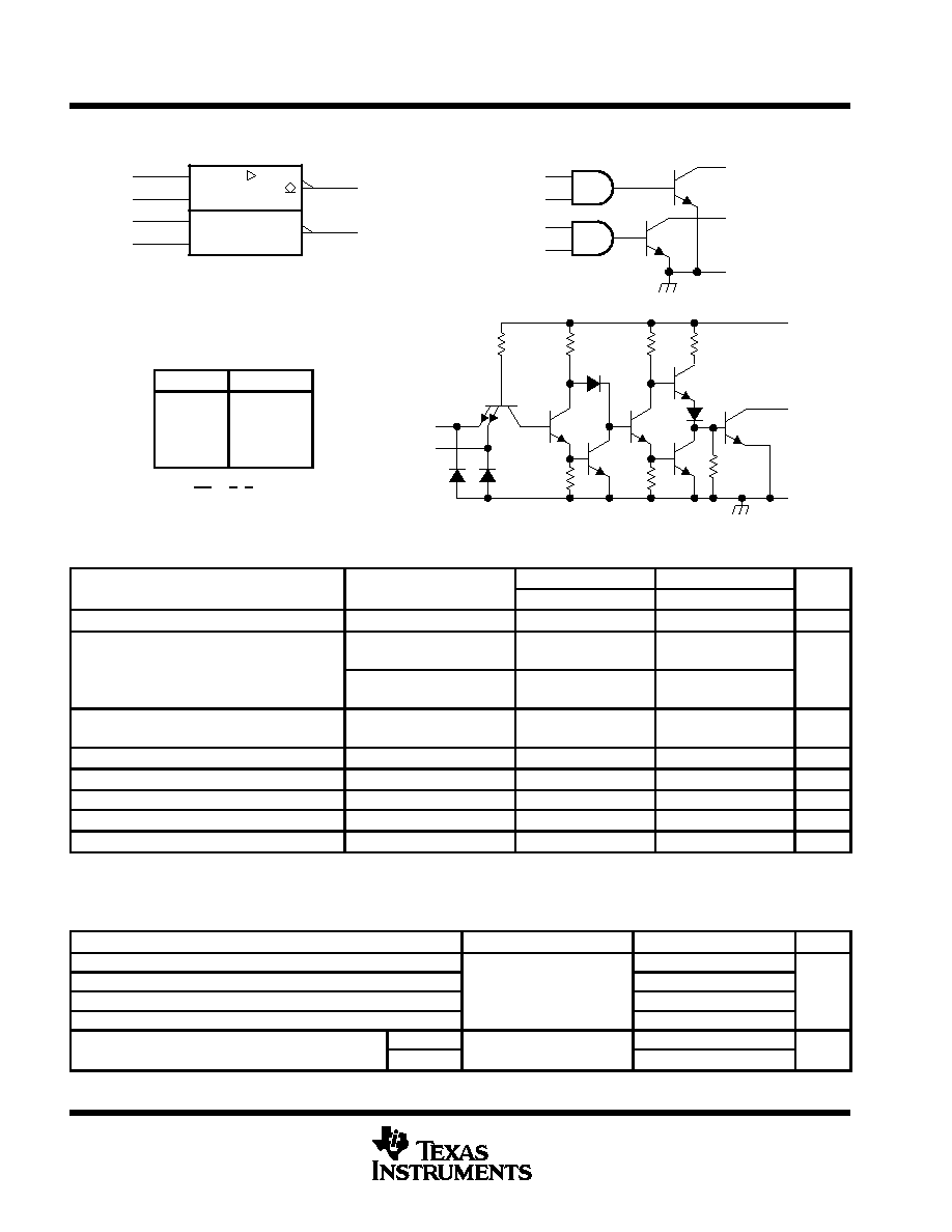
logic symbol
&
5
3
2B
2A
1B
1A
2Y
1Y
7
6
2
1
This symbol is in accordance with ANSI/IEEE Std 91-1984
and IEC publication 617-12.
Pin numbers shown are for the D, JG, and P packages.
logic diagram (positive logic)
2B
2A
1B
1A
4
5
3
GND
2Y
1Y
7
6
2
1
FUNCTION TABLE
(each driver)
A
B
Y
L
L
H (off state)
L
H
H (off state)
H
L
H (off state)
H
H
L (on state)
positive logic:
Y = AB or A+B
electrical characteristics over recommended operating free-air temperature range
PARAMETER
TEST CONDITIONS
SN55452B
SN75452B
UNIT
PARAMETER
TEST CONDITIONS
MIN
TYPß
MAX
MIN
TYPß
MAX
UNIT
VIK
Input clamp voltage
VCC = MIN,
II = ≠ 12 mA
≠ 1.2
≠ 1.5
≠ 1.2
≠ 1.5
V
VCC = MIN,
VIH = MIN,
0 25
0 5
0 25
0 4
VOL
Low level output voltage
CC
,
IOL = 100 mA
IH
,
0.25
0.5
0.25
0.4
V
VOL
Low-level output voltage
VCC = MIN,
VIH = MIN,
0 5
0 8
0 5
0 7
V
CC
,
IOL = 300 mA
IH
,
0.5
0.8
0.5
0.7
IOH
High level output current
VCC = MIN,
VIL = 0.8 V,
300
100
µ
A
IOH
High-level output current
CC
,
VOH = 30 V
IL
,
300
100
µ
A
II
Input current at maximum input voltage
VCC = MAX,
VI = 5.5 V
1
1
mA
IIH
High-level input current
VCC = MAX,
VI = 2.4 V
40
40
µ
A
IIL
Low-level input current
VCC = MAX,
VI = 0.4 V
≠ 1.1
≠ 1.6
≠ 1.1
≠ 1.6
mA
ICCH
Supply current, outputs high
VCC = MAX,
VI = 0
11
14
11
14
mA
ICCL
Supply current, outputs low
VCC = MAX,
VI = 5 V
56
71
56
71
mA
For conditions shown as MIN or MAX, use the appropriate value specified under recommended operating conditions.
ß All typical values are at VCC = 5 V, TA = 25
∞
C.
switching characteristics, V
CC
= 5 V, T
A
= 25
∞
C
PARAMETER
TEST CONDITIONS
MIN
TYP
MAX
UNIT
tPLH
Propagation delay time, low-to-high-level output
26
35
tPHL
Propagation delay time, high-to-low-level output
IO
200 mA,
CL = 15 pF,
24
35
ns
tTLH
Transition time, low-to-high-level output
O
RL = 50
,
L
See Figure 1
5
8
ns
tTHL
Transition time, high-to-low-level output
7
12
VOH
High level output voltage after switching
SN55452B
VS = 20 V,
IO
300 mA,
VS ≠ 6.5
mV
VOH
High-level output voltage after switching
SN75452B
S
,
See Figure 2
O
,
VS ≠ 6.5
mV
VCC
A
GND
Y
500
1 k
B
4 k
1.6 k
130
schematic (each driver)
Resistor values shown are nominal.
1 k
1.6 k
SN55451B, SN55452B, SN55453B, SN55454B
SN75451B, SN75452B, SN75453B, SN75454B
DUAL PERIPHERAL DRIVERS
SLRS021B ≠ DECEMBER 1976 ≠ REVISED SEPTEMBER 1999
5
POST OFFICE BOX 655303
∑
DALLAS, TEXAS 75265
logic symbol
1
5
3
2B
2A
1B
1A
2Y
1Y
7
6
2
1
This symbol is in accordance with ANSI/IEEE Std 91-1984
and IEC publication 617-12.
Pin numbers shown are for the D, JG, and P packages.
logic diagram (positive logic)
2B
2A
1B
1A
4
5
3
GND
2Y
1Y
7
6
2
1
FUNCTION TABLE
(each driver)
A
B
Y
L
L
L (on state)
L
H
H (off state)
H
L
H (off state)
H
H
H (off state)
positive logic:
Y = A+B or A B
electrical characteristics over recommended operating free-air temperature range
PARAMETER
TEST CONDITIONS
SN55453B
SN75453B
UNIT
PARAMETER
TEST CONDITIONS
MIN
TYPß
MAX
MIN
TYPß
MAX
UNIT
VIK
Input clamp voltage
VCC = MIN,
II = ≠ 12 mA
≠ 1.2
≠ 1.5
≠ 1.2
≠ 1.5
V
VCC = MIN,
VIL = 0.8 V,
0 25
0 5
0 25
0 4
VOL
Low level output voltage
CC
,
IOL = 100 mA
IL
0.25
0.5
0.25
0.4
V
VOL
Low-level output voltage
VCC = MIN,
VIL = 0.8 V,
0 5
0 8
0 5
0 7
V
CC
,
IOL = 300 mA
IL
0.5
0.8
0.5
0.7
IOH
High level output current
VCC = MIN,
VIH = MIN,
300
100
µ
A
IOH
High-level output current
CC
,
VOH = 30 V
IH
,
300
100
µ
A
II
Input current at maximum input voltage
VCC = MAX,
VI = 5.5 V
1
1
mA
IIH
High-level input current
VCC = MAX,
VI = 2.4 V
40
40
µ
A
IIL
Low-level input current
VCC = MAX,
VI = 0.4 V
≠ 1
≠ 1.6
≠ 1
≠ 1.6
mA
ICCH
Supply current, outputs high
VCC = MAX,
VI = 5 V
8
11
8
11
mA
ICCL
Supply current, outputs low
VCC = MAX,
VI = 0
54
68
54
68
mA
For conditions shown as MIN or MAX, use the appropriate value specified under recommended operating conditions.
ß All typical values are at VCC = 5 V, TA = 25
∞
C.
switching characteristics, V
CC
= 5 V, T
A
= 25
∞
C
PARAMETER
TEST CONDITIONS
MIN
TYP
MAX
UNIT
tPLH
Propagation delay time, low-to-high-level output
18
25
tPHL
Propagation delay time, high-to-low-level output
IO
200 mA,
CL = 15 pF,
18
25
ns
tTLH
Transition time, low-to-high-level output
O
,
RL = 50
,
L
,
See Figure 1
5
8
ns
tTHL
Transition time, high-to-low-level output
7
12
VOH
High level output voltage after switching
SN55453B
VS = 20 V,
IO
300 mA,
VS ≠ 6.5
mV
VOH
High-level output voltage after switching
SN75453B
S
See Figure 2
O
VS ≠ 6.5
mV
schematic (each driver)
Resistor values shown are nominal.
VCC
A
GND
Y
500
1 k
B
4 k
1.6 k
130
4 k