TAS5012
SLES006A ≠ SEPTEMBER 2001 ≠ REVISED DECEMBER 2001
TRUE DIGITAL AUDIO AMPLIFIER
TAS5012 DIGITAL AUDIO PWM PROCESSOR
1
www.ti.com
FEATURES
D
TAS5012 + TAS5110 TDAA System ≠ High
Quality Digital Audio Amplification
D
102-dB Dynamic Range (TAS5012 Device)
D
THD+N < 0.06%
D
Power Efficiency Is 90% Into 8-
Load
D
16-, 20-, or 24-Bit Input Data
D
32-kHz, 44.1-kHz, 48-kHz, 88.2-kHz, 96-kHz,
176.4-kHz, 192-kHz Sampling Rates
D
Economical 48-Pin TQFP Package
D
Lower-Jitter Internal PLL
D
3.3-V Power Supply
D
Mute
D
Clicks and Pops Reduction (Patent Pending)
APPLICATIONS
D
DVD-Audio
D
Home Theater
D
Car Audio Amplifiers and Head Units
D
Internet Music Appliance
D
Mini/Micro Component Systems
DESCRIPTION
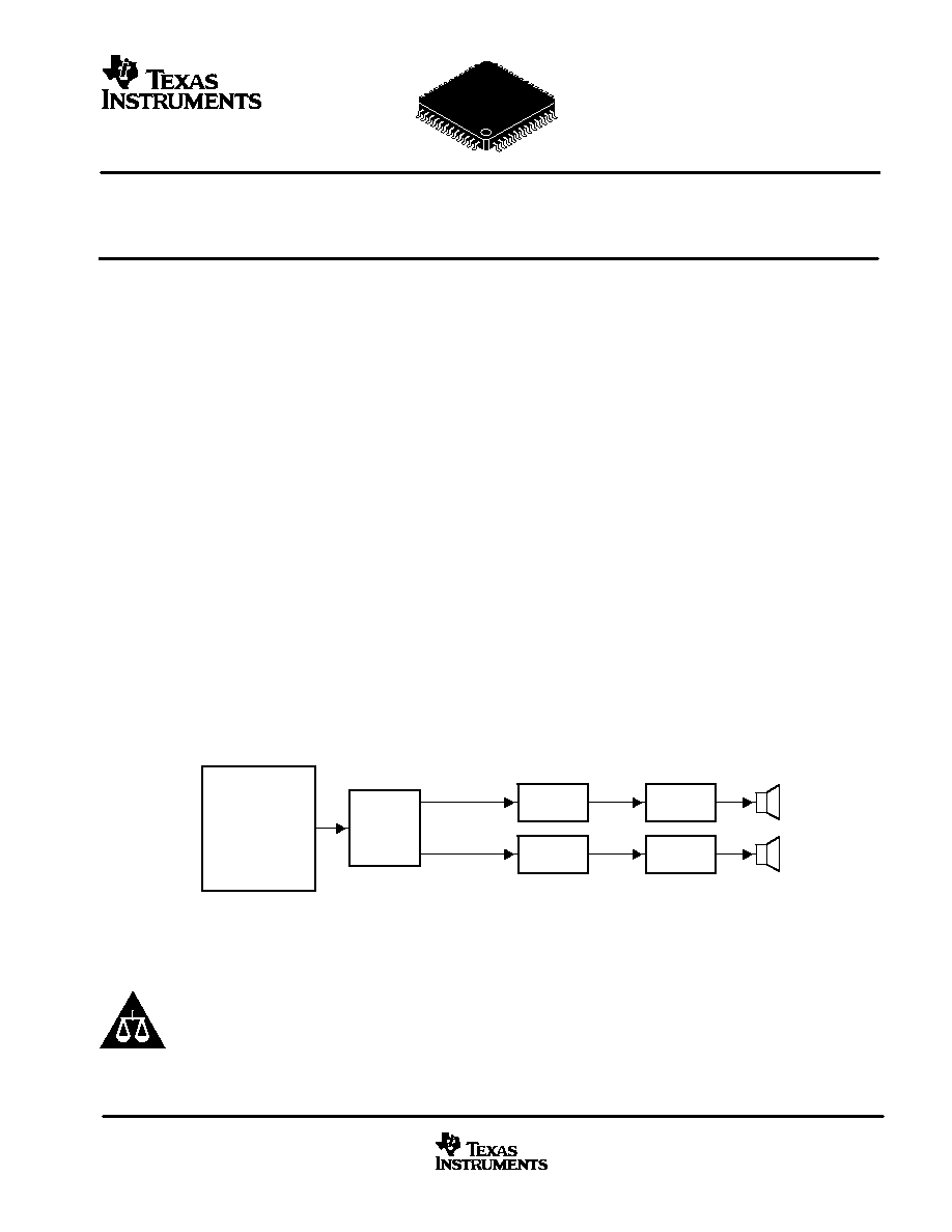
True digital audio amplifier (TDAA) is a new paradigm in digital audio. One TDAA system consists of the TAS5012
PCM-PWM modulator device + TAS5110 PWM power output device. This system accepts a serial PCM digital audio
stream and converts it to a 3.3-V PWM audio stream (TAS5012). The TAS5110 device then provides a large-signal
PWM output. This digital PWM signal is then demodulated providing power output for driving loudspeakers. This
patented technology provides low-cost, high-quality, high-efficiency digital audio applicable to many audio systems
developed for the digital age. The TAS5012 is an innovative, cost-effective, high-performance 24-bit stereo
PCM-PWM modulator based on Equibit
technology. It has a wide variety of serial input options including
right-justified (16, 20, or 24 bits), IIS (16, 20, or 24 bits), left-justified (16 bits), or DSP (16 bits) data formats. It is fully
compatible with AES standard sampling rates of 32 kHz, 44.1 kHz, 48 kHz, 88.2 kHz, 96 kHz, 176.4 kHz, and 192 kHz.
The TAS5012 also provides a de-emphasis function for 44.1-kHz and 48-kHz sampling rates.
TAS5012
TAS5110
Left
∑
Volume
∑
EQ
∑
DRC
∑
Bass
∑
Treble
∑
Serial Audio Input Port
∑
Internal PLL
∑
Equibit
Modulator
∑
Up to 192-kHz Input
Sampling Rate
∑
TAS3001
∑
DSP
∑
S/PDIF
∑
1394
Digital Audio
∑
H-Bridges
Power Devices
∑
Improved Performance
From TAS5100
TAS5110
Right
L-C
Filter
L-C
Filter
Please be aware that an important notice concerning availability, standard warranty, and use in critical applications of
Texas Instruments semiconductor products and disclaimers thereto appears at the end of this data sheet.
PRODUCTION DATA information is current as of publication date.
Products conform to specifications per the terms of Texas Instruments
standard warranty. Production processing does not necessarily include
testing of all parameters.
Copyright
2001, Texas Instruments Incorporated
Equibit is a trademark of Toccata Technology ApS, Denmark.
All other trademarks are the property of their respective owners.
TAS5012
SLES006A ≠ SEPTEMBER 2001 ≠ REVISED DECEMBER 2001
2
www.ti.com
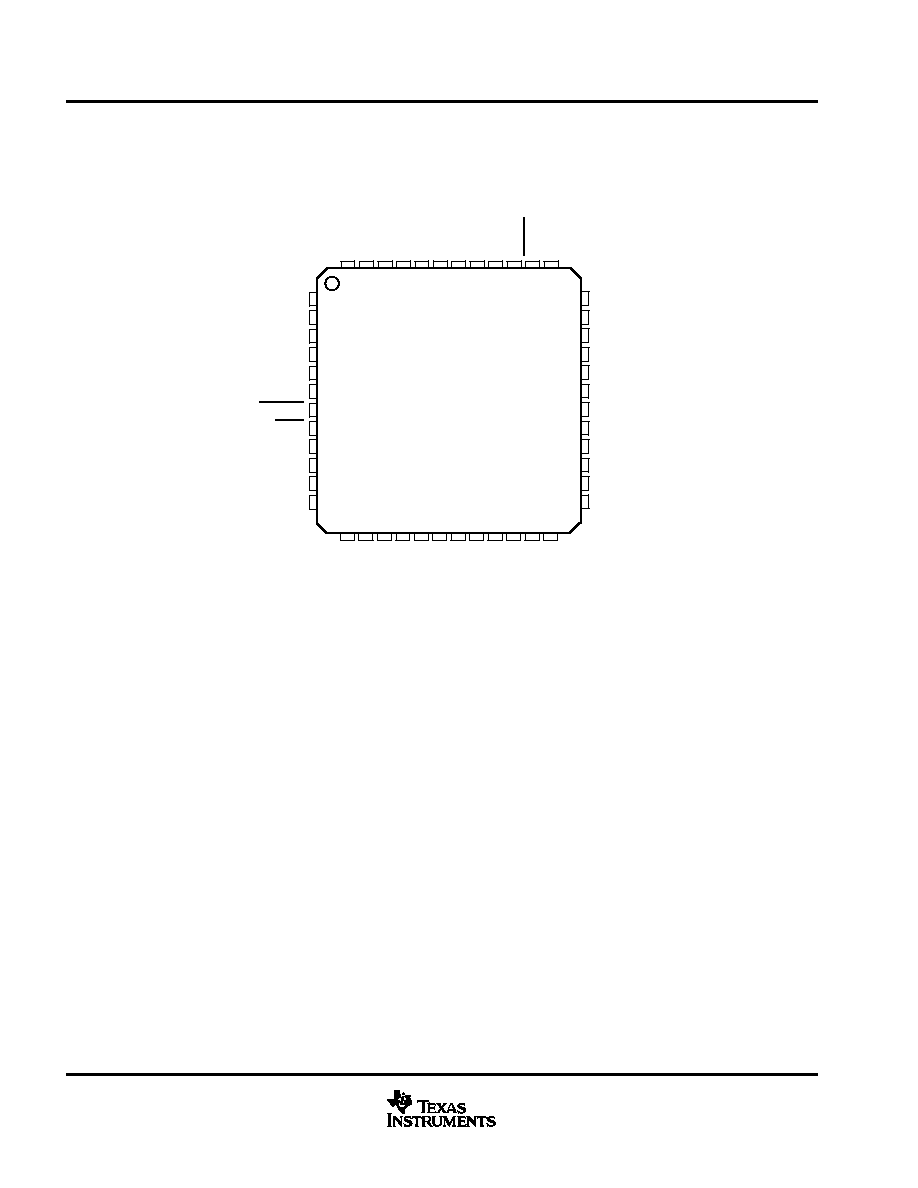
terminal assignments
14 15
DVDD3_L
PWM_AP_L
PWM_AM_L
PWM_BM_L
PWM_BP_L
DVDD2
DVSS2
PWM_AP_R
PWM_AM_R
PWM_BM_R
PWM_BP_R
DVDD3_R
36
35
34
33
32
31
30
29
28
27
26
25
16
1
2
3
4
5
6
7
8
9
10
11
12
MCLK_IN
AVDD2
PLL_FLT_OUT
PLL_FLT_RET
AVSS2
NC
RESET
PDN
VALID_R
M_S
NC
DVDD1
17 18 19 20
47 46 45 44 43
48
42
40 39 38
41
21 22 23 24
37
13
48-Pin LQFP PACKAGE
(TOP VIEW)
NC ≠ No internal connection
A
VDD1
XTL_IN
XTL_OUT
OSC_CAP
A
VSS1
DEM_EN
DEM_SEL
FTEST
STEST
DBSPD
MUTE
DVSS3_L
DVSS1
DVDD1
DVSS1
MCLK_OUT
SCLK
LRCLK
SDIN
MOD2
MOD1
MOD0
V
ALID_L
DVSS3_R
references
D
True Digital Audio Amplifier TAS5100 PWM Power Output Stage data sheet ≠ Texas Instruments literature
number SLLS419
D
Design Considerations for TAS5000/TAS5110 True Digital Audio Power Amplifiers data sheet ≠ Texas
Instruments literature number SLAA117
D
Digital Audio Measurements application note ≠ Texas Instruments literature number SLAA114
D
PowerPAD
Thermally Enhanced Package application note ≠ Texas Instruments literature
number SLMA002
PowerPAD is a trademark of Texas Instruments.

TAS5012
SLES006A ≠ SEPTEMBER 2001 ≠ REVISED DECEMBER 2001
3
www.ti.com
functional block diagram
PLL/Clock
Generator
OSC
Serial
Audio
Port
Digital
Interpolation
Filter
Equibit
Modulator
Buffer
Audio Port
Configuration
Control Section
LRCLK
SCLK
SDIN
PWM_AP_L
PWM_AM_L
PLL_FL
T_RET
PLL_FL
T_OUT
MCLK_IN
MCLK_OUT
XTL_IN
XTL_OUT
OSC_CAP
MOD0
MOD1
MOD2
DEM_SEL
DEM_EN
MUTE
RESET
PDN
FTEST
STEST
DBSPD
M_S
DVDD1
DVSS1
DVDD2
DVSS2
DVDD3_L
DVSS3_L
DVDD3_R
DVSS3_R
A
VDD1
A
VSS1
A
VDD2
A
VSS2
PWM_AP_R
PWM_AM_R
V
ALID_R
V
ALID_L
PWM_BP_L
PWM_BM_L
PWM_BP_R
PWM_BM_R
ordering information
TA
PACKAGE
0
∞
C to 70
∞
C
TAS5012PFB
≠40
∞
C to 85
∞
C
TAS5012IPFB
NOTE: These packages are available taped and reeled. Add R suffix
to ordering number (e.g., TAS5012PFBR).
TAS5012
SLES006A ≠ SEPTEMBER 2001 ≠ REVISED DECEMBER 2001
4
www.ti.com
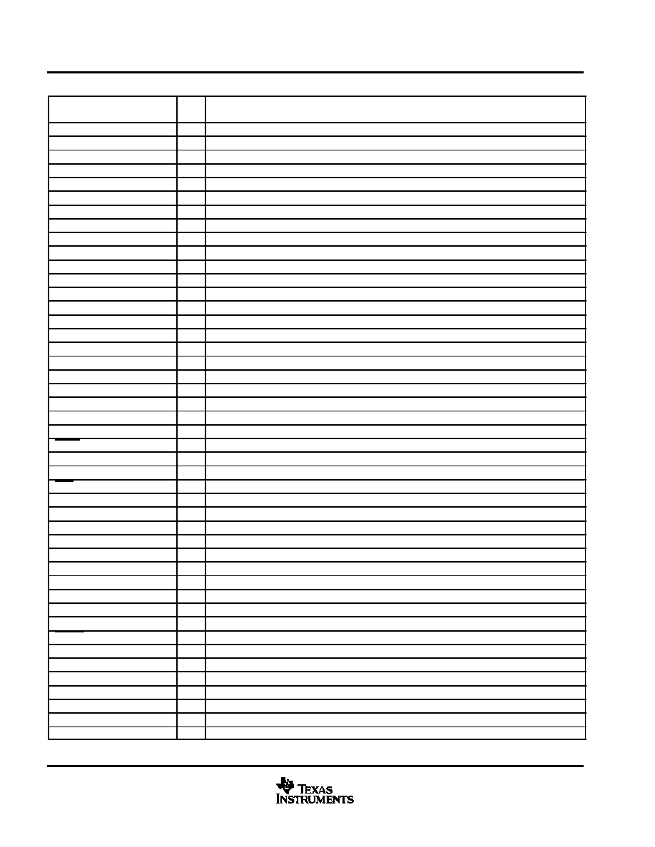
Terminal Functions
TERMINAL
I/O
DESCRIPTION
NAME
NO.
I/O
DESCRIPTION
AVDD1
48
I
Analog supply for oscillator
AVDD2
2
I
Analog supply for PLL
AVSS1
44
I
Analog ground for oscillator
AVSS2
5
I
Analog ground for PLL
DBSPD
39
I
Indicates sample rate is double speed (88.2 kHz or 96 kHz), active high
DEM_EN
43
I
De-emphasis enable, active high
DEM_SEL
42
I
De-emphasis select (0 = 44.1 kHz, 1 = 48 kHz)
DVDD1
12, 14
I
Digital voltage supply for logic
DVDD2
31
I
Digital voltage supply for PWM reclocking
DVDD3_L
36
I
Digital voltage supply for PWM output (left)
DVDD3_R
25
I
Digital voltage supply for PWM output (right)
DVSS1
13, 15
I
Digital ground for logic
DVSS2
30
I
Digital ground for PWM reclocking
DVSS3_L
37
I
Digital ground for PWM output (left)
DVSS3_R
24
I
Digital ground for PWM output (right)
FTEST
41
I
Tied to DVSS1 for normal operation
LRCLK
18
I/O
Left/right clock (input when M_S = 0; output when M_S = 1)
MCLK_IN
1
I
MCLK input
MCLK_OUT
16
O
Buffered system clock output if M_S = 1; otherwise set to 0
MOD0
22
I
Serial interface selection pin, bit 0
MOD1
21
I
Serial interface selection pin, bit 1
MOD2
20
I
Serial interface selection pin, bit 2 (MSB)
M_S
10
I
Master/slave, master=1, slave=0
MUTE
38
I
Muted signal = 0, normal mode = 1
NC
6, 11
No connection
OSC_CAP
45
I
Oscillator cap return
PDN
8
I
Power down, active low
PLL_FLT_OUT
3
O
Output terminal for external PLL filter
PLL_FLT_RET
4
I
Return for external PLL filter
PWM_AM_L
34
O
PWM left output A (differential ≠)
PWM_AM_R
28
O
PWM right output A (differential ≠)
PWM_AP_L
35
O
PWM left output A (differential +)
PWM_AP_R
29
O
PWM right output A (differential +)
PWM_BM_L
33
O
PWM left output B (differential ≠)
PWM_BM_R
27
O
PWM right output B (differential ≠)
PWM_BP_L
32
O
PWM left output B (differential +)
PWM_BP_R
26
O
PWM right output B (differential +)
RESET
7
I
Reset (active low)
SCLK
17
I/O
Shift clock (input when M_S = 0, output when M_S = 1)
SDIN
19
I
Stereo serial audio data input
STEST
40
I
Tied to DVSS1 for normal operation
VALID_L
23
O
PWM left outputs valid (active high)
VALID_R
9
O
PWM right outputs valid (active high)
XTL_IN
47
I
Crystal or clock input (MCLK input)
XTL_OUT
46
O
Crystal output (not for external usage). NC when XTL_IN is MCLK input
TAS5012
SLES006A ≠ SEPTEMBER 2001 ≠ REVISED DECEMBER 2001
5
www.ti.com
functional description
serial audio port
The serial audio port consists of a shift clock (SCLK pin), a left/right frame synchronization clock (LRCLK pin), and
a data input (SDIN pin). The serial audio port supports standard serial PCM formats (Fs = 32 kHz, 44.1 kHz, 48 kHz,
88.2 kHz, 96 kHz, 176.4 kHz, or 192 kHz) stereo. See the serial interface formats section.
system clocks--master mode and slave mode
The TAS5012 allows multiple system clocking schemes. In this document, master mode indicates that the TAS5012
provides system clocks to other parts of the system (M_S=1). Audio system clocks of frequency 256 Fs MCLK_OUT,
64 Fs SCLK, and Fs LRCLK are output from this device when it is configured in master mode. Slave mode indicates
that a system master other than the TAS5012 provides system clocks (LRCLK, SCLK, and MCLK_IN) to the TAS5012
(M_S = 0). The TAS5012 operates with LRCLK and SCLK synchronized to MCLK. TAS5012 does not require any
specific phase relationship between LRCLK and MCLK, but there must be synchronization. In the slave mode
MCLK_OUT is driven low. Table 1 shows all the possible master and slave modes. When operating in quad mode
(Fs = 176.4 kHz or 192 kHz), the device works in slave mode only with MCLK_IN = 128 Fs.
oscillator/sampling frequency
The sampling frequency is determined by the crystal (master mode) or master clock in (slave mode) which should
be either 8.192 MHz (Fs = 32 kHz), 11.2896 MHz (Fs = 44.1 kHz), or 12.288 MHz (Fs = 48 kHz). Twice the
normal sampling frequency can be selected by using the DBSPD pin which allows usage of Fs = 88.2 kHz or Fs
= 96 kHz. In the double-speed slave mode (DBSPD = 1, M_S = 0), the external clock input is either 22.5796 MHz
(Fs = 88.2 kHz) or 24.576 MHz (Fs = 96 kHz). Note that 32-kHz sampling is supported in the normal speed
modes. Table 1 explains the proper clock selection.
Table 1. Oscillator, External Clock, and PLL Functions
DESCRIPTION
M_S
DBSPD
XTL_IN
(MHz)
MCLK_IN
(MHz)
SCLK
(MHz)∂
LRCLK
(kHz)∂
MCLK_OUT
(MHz)#
Master, normal speed
1
0
8.192
--
2.048
32
8.192
Master, normal speed
1
0
11.2896
--
2.8224
44.1
11.2896
Master, normal speed
1
0
12.288
--
3.072
48
12.288
Master, double speed
1
1
--
22.5792ß
5.6448
88.2
22.5792
Master, double speed
1
1
--
24.576ß
6.144
96
24.576
Slave, normal speed
0
0
--
8.192ß
2.048
32
Digital GND
Slave, normal speed
0
0
--
11.2896ß
2.8224
44.1
Digital GND
Slave, normal speed
0
0
--
12.288ß
3.072
48
Digital GND
Slave, double speed
0
1
--
22.5792ß
5.6448
88.2
Digital GND
Slave, double speed
0
1
--
24.576ß
6.144
96
Digital GND
Slave, quad speed||
0
0
--
22.5792ß
11.2896
176.4
Digital GND
Slave, quad speed||
0
0
--
24.576ß
12.288
192
Digital GND
Either a crystal oscillator or an external clock of the specified frequency can be connected to XTL_IN.
MCLK_IN tied low when input to XTL_IN is provided; XTL_IN tied low when MCLK_IN is provided.
ß External MCLK connected to MCLK_IN input
∂ SCLK and LRCLK are outputs when M_S = 1, inputs when M_S = 0.
# MCLK_OUT is driven low when M_S = 0.
|| Quad speed mode is detected automatically. when DBSPD = 0.
phase-locked loop (PLL)/clock generation
A low jitter PLL is incorporated for internal use. Connections for the PLL external loop filter are provided as
PLL_FLT_RET and PLL_FLT_OUT. If the PLL loses lock, the PWM output status pins (VALID_L and VALID_R) go
low. Note that VALID_L and VALID_R can go low for other conditions as well. See the error status reporting section.
TAS5012
SLES006A ≠ SEPTEMBER 2001 ≠ REVISED DECEMBER 2001
6
www.ti.com
functional description (continued)
digital interpolation filter
The 24-bit high-performance linear phase FIR interpolation filter up-samples the input digital data at a rate of two
times (quad speed mode = 176.4 kHz or 192 kHz), four times (double speed mode = 88.2 kHz or 96 kHz), or eight
times (normal mode = 32 kHz, 44.1 kHz, or 48 kHz) the incoming sample rate. This filter provides very low pass-band
ripple and optimized time domain transient response for accurate music reproduction.
digital PWM modulator
The interpolation filter output is sent to the modulator. This modulator consists of a high performance fourth order
digital noise shaper and a PCM-to-PWM converter. Following the noise shaper, the PCM signal is fed into a very low
distortion PCM-to-PWM conversion block, buffered, and output from the chip. The modulation scheme is based on
a 2-state control of the H-bridge output.
control, status, and operational modes
The TAS5012 control section consists of several control-input pins. Three serial mode pins (MOD0, MOD1, and
MOD2) are provided to select various serial data formats. During normal operating conditions if any of the MOD0,
MOD1, or MOD2 pins changes state, a reset sequence is initiated. Also provided are separate power-down (PDN),
reset (RESET), and mute (MUTE) pins.
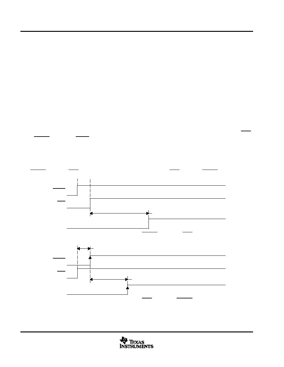
power up
At power up the VALID_L and VALID_R pins are asserted low and the PWM outputs go to the hard mute state in which
the P outputs are held low and the M outputs are held high. Following initialization, the TAS5012 comes up in the
operational state (differential PWM audio). There are two cases of power-up timing. The first case is shown in Figure 1
with RESET preceding PDN. The second case is shown in Figure 2 with PDN preceding RESET.
Initialization Time = 100 ms max
RESET
PDN
VALID_L
VALID_R
Figure 1. Power-Up Timing (RESET Preceding PDN)
Initialization Time = 5 ms max
RESET
PDN
Greater Than 16 MCLK Periods
VALID_L
VALID_R
Figure 2. Power-Up Timing (PDN Preceding RESET)
TAS5012
SLES006A ≠ SEPTEMBER 2001 ≠ REVISED DECEMBER 2001
7
www.ti.com
functional description (continued)
reset
The reset signal for the TAS5012 must be applied whenever toggling the M_S, DBSPD signal. This reset is
asynchronous. See Figure 3 for reset timing. To initiate the reset sequence the RESET pin is asserted low. As long
as the pin is held low, the chip is in the reset state. During this reset time the PWM outputs are hard-muted (P-outputs
held low and M-outputs held high) and the PWM outputs valid pins (VALID_L. VALID_R) are held low. Assuming PDN
is high, the rising edge of the reset pulse begins chip initialization. After the initialization time, the TAS5012 begins
normal operation.
Initialization
Normal
Operation
RESET
PDN
Normal Operation
5 ms max
VALID_L
VALID_R
Figure 3. Reset Timing
power down
When PDN is low (see Figure 4), both the PLL and the oscillator are shut down. Note that power down is an
asynchronous operation. To place the device in total power-down mode, both RESET and PDN must be held low.
As long as these pins are held low, the chip is in the power-down state and the PWM outputs are hard muted with
the P outputs held low and the M outputs held high. To place the device back into normal mode, see the power up
section.
NOTE: In order for the dynamic logic to be properly powered down, the clocks should not be stopped before the PDN
pin goes low. Otherwise, the device may drain additional supply current.
Initialization
Chip
Power-Down
PDN and RESET
Normal Operation
Normal
Operation
VALID
Figure 4. Power-Down Timing
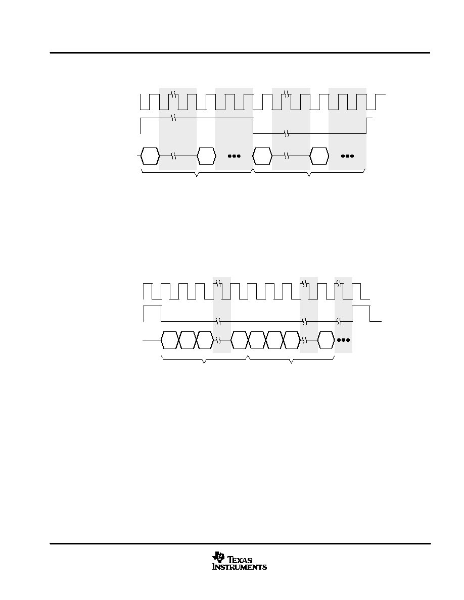
mute
The TAS5012 provides a mute function that is used when the MUTE pin is asserted low. See Table 2 for mute
description. This mute is a quiet mute; that is, the mute is accomplished by outputting a zero value waveform in which
both sides of the differential PWM outputs have a 50% duty cycle (see Figure 5 for mute timing).
Table 2. Mute Description
MUTE
P OUTPUTS
M OUTPUTS
DESCRIPTION
0
50% duty cycle
50% duty cycle
Mute
1
DATA
DATA
Normal operation

TAS5012
SLES006A ≠ SEPTEMBER 2001 ≠ REVISED DECEMBER 2001
8
www.ti.com
functional description (continued)
Initialization
Normal State
MUTE
VALID_L
5 ms max
10
µ
s Maximum
50≠50 Duty Cycle
(P, M Complementary)
Inactive State
VALID_R
PWM Outputs
(P, M Complementary)
Figure 5. Mute Timing
double speed
Double-speed mode is used to support sampling rates of 88.2 kHz and 96 kHz. In order to put the TAS5012 in
double-speed mode with the device in normal operating conditions, the RESET pin must be held low while switching
the DBSPD pin high. After the RESET pin is brought high again, a reset sequence takes place. If the change is at
power up, a power-up sequence is originated.
quad speed
Quad-speed mode is used to support sampling rates of 176.4 kHz and 192 kHz. It is supported in slave mode only.
In order to put the TAS5012 in quad-speed mode, M_S and DBPSB pins are brought low. Quad-speed mode is then
automatically detected due to the fact that it is the only mode in which MCLK_IN is 128Fs. DEM_SEL must be set
to low when operating in the quad-speed mode.
de-emphasis filter
For audio sources that have been preemphasized, a precision 50-
µ
s/15-
µ
s de-emphasis filter is provided to support
the sampling rates of 44.1 kHz and 48 kHz. Pins DEM_SEL and DEM_EN select the de-emphasis functions. See
Figure 6 for a graph showing the de-emphasis filtering characteristics. See Table 3 for de-emphasis selection.
0
≠10
Response
≠
dB
3.18 (50
µ
s)
10.6 (15
µ
s)
f ≠ Frequency ≠ kHz
De-emphasis
Figure 6. De-Emphasis Filter Characteristics

TAS5012
SLES006A ≠ SEPTEMBER 2001 ≠ REVISED DECEMBER 2001
9
www.ti.com
functional description (continued)
de-emphasis selection
De-emphasis selection is accomplished by using the DEM_SEL and DEM_EN pins. See Table 3 for de-emphasis
selection description.
Table 3. De-Emphasis Selection
DEM_SEL
DEM_EN
DESCRIPTION
0
0
De-emphasis disabled
0
1
De-emphasis enabled for Fs = 44.1 kHz
1
1
De-emphasis enabled for Fs = 48 kHz
1
0
Forbidden state. Do not use.
error status reporting (VALID_L and VALID_R)
The following is a list of the error conditions that will cause the VALID_L and VALID_R pins to be asserted low:
D
No clocks
D
Clock phase errors
When either of the above conditions is met, the VALID_L and VALID_R goes low and the PWM outputs go to the hard
mute state. If the error condition is removed, the TAS5012 is reinitialized and the VALID_L and VALID_R pins are
asserted high.
serial interface formats
The TAS5012 is compatible with eight different serial interfaces. Available interface options are IIS, right justified, left
justified, and DSP frame. Table 4 indicates how these options are selected using the MOD0, MOD1, and MOD2 pins.
Table 4. Hardware Selection of Serial Audio Modes
MODE
MOD2 PIN
MOD1 PIN
MOD0 PIN
SERIAL INTERFACE
SDIN
0
0
0
0
16 bit, MSB first; right justified
1
0
0
1
20 bit, MSB first; right justified
2
0
1
0
24 bit, MSB first; right justified
3
0
1
1
16 bit IIS
4
1
0
0
20 bit IIS
5
1
0
1
24 bit IIS
6
1
1
0
16 bit MSB first, left justified
7
1
1
1
16 bit DSP frame
The following figures illustrate the relationship between the SCLK, LRCLK and the serial data I/O for the different
interface protocols. Note that there are always 64 SCLKs per LRCLK. The nondata bits are padded with binary 0s.

TAS5012
SLES006A ≠ SEPTEMBER 2001 ≠ REVISED DECEMBER 2001
10
www.ti.com
functional description (continued)
MSB first, right-justified (for 16, 20, 24 bits)
X
MSB
LSB
MSB
LSB
SCLK
LRCLK = Fs
SDIN
Left Channel
Right Channel
X
Figure 7. MSB First Right Justified
Note the following characteristics of this protocol:
D
Left channel is received when LRCLK is high.
D
Right channel is received when LRCLK is low.
D
SDIN is sampled at the rising edge of SCLK.
IIS compatible serial format (for 16, 20, 24 bits)
X
MSB
LSB
X
MSB
LSB
SCLK
LRCLK = Fs
SDIN
Left Channel
Right Channel
Figure 8. IIS Compatible Serial Format
Note the following characteristics of this protocol:
D
Left channel is received when LRCLK is low.
D
Right channel is received when LRCLK is high.
D
SDIN is sampled with the rising edge of the SCLK.
TAS5012
SLES006A ≠ SEPTEMBER 2001 ≠ REVISED DECEMBER 2001
11
www.ti.com
functional description (continued)
MSB left-justified serial interface format (for 16 bits)
MSB
LSB
MSB
LSB
SCLK
LRCLK = Fs
SDIN
Left Channel
Right Channel
Figure 9. MSB Left-Justified Serial Interface Format
Note the following characteristics of this protocol:
D
Left channel is received when LRCLK is high.
D
Right channel is received when LRCLK is low.
D
SDIN is sampled at the rising edge of SCLK.
DSP compatible serial interface format (for 16 bits)
SCLK
LRCLK = Fs
SDIN
Left Channel
(MSB = 15)
Right Channel
(MSB = 15)
15
14
13
0
15
14
13
0
Figure 10. DSP Compatible Serial Interface Format
Note the following characteristic of this protocol:
D
Serial data is sampled with the falling edge of SCLK.
PWM Outputs
Designed to be used with the TAS5110 family of H-bridges, the PWM outputs provide differential 3.3-V square-wave
signals. During normal operation these outputs represent the input PCM audio in the pulse-width modulation scheme.
In the hard-mute state the P outputs (PWM_AP_L, PWM_BP_L, PWM_AP_R, and PWM_BP_R) are held low and
the M outputs (PWM_AM_L, PWM_BM_L, PWM_AM_R, and PWM_BM_R) are held high. In the quiet-mute state
the differential PWM outputs have a 50% duty cycle.
TAS5012
SLES006A ≠ SEPTEMBER 2001 ≠ REVISED DECEMBER 2001
12
www.ti.com
absolute maximum ratings over operating free-air temperature (unless otherwise noted)
Analog supply voltage range, AVDD1, AVDD2
≠ 0.3 V to 4.2 V
. . . . . . . . . . . . . . . . . . . . . . . . . . . . . . . . . . . . . . . . . . . . .
Digital power supply voltage, DVDD1, DVDD2, DVDD3_L, DVDD3_R
≠ 0.3 V to 4.2 V
. . . . . . . . . . . . . . . . . . . . . . . . .
Digital input voltage, V
I
(see Note 1)
≠ 0.3 V to DVDDX
+ 0.3 V
. . . . . . . . . . . . . . . . . . . . . . . . . . . . . . . . . . . . . . . . . . . .
Operating free-air temperature, T
A
0
∞
C to 70
∞
C
. . . . . . . . . . . . . . . . . . . . . . . . . . . . . . . . . . . . . . . . . . . . . . . . . . . . . . . . . .
Storage temperature, T
stg
≠ 65
∞
C to 150
∞
C
. . . . . . . . . . . . . . . . . . . . . . . . . . . . . . . . . . . . . . . . . . . . . . . . . . . . . . . . . . . . . .
ESD
2000 V
. . . . . . . . . . . . . . . . . . . . . . . . . . . . . . . . . . . . . . . . . . . . . . . . . . . . . . . . . . . . . . . . . . . . . . . . . . . . . . . . . . . . . . . . .
Stresses beyond those listed under "absolute maximum ratings" may cause permanent damage to the device. These are stress ratings only, and
functional operation of the device at these or any other conditions beyond those indicated under "recommended operating conditions" is not
implied. Exposure to absolute-maximum-rated conditions for extended periods may affect device reliability.
NOTE 1: DVDD1, DVDD2, DVDD3_L, DVDD3_R.
recommended operating conditions,
T
A
= 25
∞
C, DVDD1 = DVDD2 = DVDD3_L = DVDD3_R = 3.3 V
±
10%,
AVDD1 = AVDD2 = 3.3 V
±
10%, Fs = 44.1 kHz
MIN
TYP
MAX
UNIT
Supply voltage
Digital
DVDDX
3
3.3
3.6
V
Supply current
Digital
Operating
22
mA
Supply current
Digital
Power downß
10
20
µ
A
Power dissipation
Digital
Operating
59.4
mW
Power dissipation
Digital
Power downß
6.6
72
µ
W
Supply voltage
Analog
AVDDX∂
3
3.3
3.6
V
Supply current
Analog
Operating
8
mA
Supply current
Analog
Power downß
10
100
µ
A
Power dissipation
Analog
Operating
26.4
mW
Power dissipation
Analog
Power downß
33
360
µ
W
DVDD1, DVDD2, DVDD3_L, DVDD3_R
ß If the clocks are turned off
∂ AVDD1, AVDD2
electrical characteristics, T
A
= 25
∞
C, DVDD1 = DVDD2 = DVDD3_L = DVDD3_R = 3.3 V
±
10%,
AVDD1 = AVDD2 = 3.3 V
±
10%
static digital specifications
MIN
MAX
UNIT
VIH
High-level input voltage
2
DVDD1
V
VIL
Low-level input voltage
0
0.8
V
VOH
High-level output voltage, (IO = ≠1 mA)
2.4
V
VOL
Low-level output voltage, (IO = 4 mA)
0.4
V
Input leakage current
≠10
10
µ
A
digital interpolation filter and PWM modulator, Fs = 44.1 kHz
MIN
TYP
MAX
UNIT
Pass band
0
20
kHz
Pass-band ripple
±
0.012
dB
Stop band
24.1
kHz
Stop-band attenuation (24.1 kHz to 152.3 kHz)
50
dB
Group delay
700
µ
S
PWM modulation index (gain)
0.93

TAS5012
SLES006A ≠ SEPTEMBER 2001 ≠ REVISED DECEMBER 2001
13
www.ti.com
TAS5012/TAS5110 system performance measured at the speaker terminals
See application note SLAA117.
switching characteristics,
T
A
= 25
∞
C, DVDD1 = DVDD2 = DVDD3_L = DVDD3_R = AVDD1 = AVDD2 = 10% 3.3 V
±
10%
serial audio ports slave mode
PARAMETER
MIN
TYP
MAX
UNIT
f(SCLK)
SCLK frequency
12.288
MHz
tsu(SDIN)
SDIN setup time before SCLK rising edge
20
ns
th(SDIN)
SDIN hold time from SCLK rising edge
10
ns
f(LRCLK)
LRCLK frequency
32
48
192
kHz
MCLK duty cycle
50%
SCLK duty cycle
50%
LRCLK duty cycle
50%
tsu(LRCLK)
LRCLK edge setup before SCLK rising edge
20
ns
serial audio ports master mode, load conditions = 50 pF
PARAMETER
MIN
TYP
MAX
UNIT
t(MSD)
MCLK to SCLK
0
5
ns
t(MLRD)
MLCK to LRCLK
0
5
ns
DSP serial interface mode
PARAMETER
MIN
TYP
MAX
UNIT
f(SCLK)
SCLK frequency
12.288
MHz
tw(FSHIGH)
Pulse duration, sync
1/(64
◊
Fs)
ns
tsu(SDIN),
tsu(LRCLK)
SDIN and LRCLK setup time before SCLK falling edge
20
ns
th(SDIN),
th(LRCLK)
SDIN and LRCLK hold time from SCLK falling edge
10
ns
SCLK duty cycle
50%

TAS5012
SLES006A ≠ SEPTEMBER 2001 ≠ REVISED DECEMBER 2001
14
www.ti.com
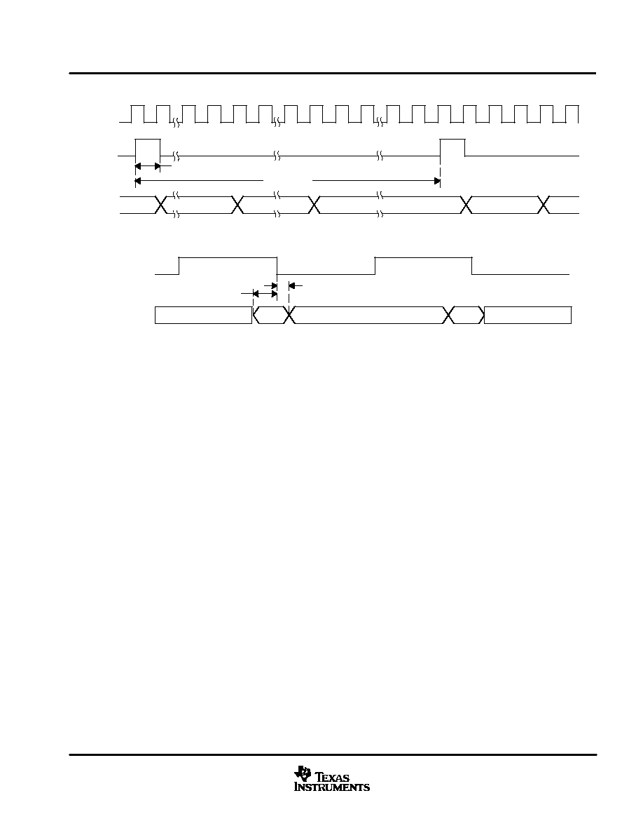
PARAMETER MEASUREMENT INFORMATION
ŒŒŒŒŒŒŒ
ŒŒŒŒŒŒŒ
th(SDIN)
tsu(SDIN)
SCLK
SDIN
Figure 11. Right-Justified, IIS, Left-Justified Serial Protocol Timing
tsu(LRCLK)
SCLK
LRCLK
NOTE: Serial data is sampled with the rising edge of SCLK (setup time = 20 ns and hold time = 10 ns)
Figure 12. Right, Left, and IIS Serial Mode Timing Requirement
t(MSD)
t(MLRD)
SCLK
LRCLK
(Output)
MCLK
(Output)
Figure 13. Serial Audio Ports Master Mode Timing
ŒŒŒŒŒŒŒŒŒŒŒŒ
ŒŒŒŒŒŒŒŒŒŒŒŒ
th(SDIN)
tsu(SDIN)
SCLK
LRCLK
SDIN
tsu(LRCLK)
tw(FSHIGH)
th(LRCLK)
Figure 14. DSP Serial Port Timing
TAS5012
SLES006A ≠ SEPTEMBER 2001 ≠ REVISED DECEMBER 2001
15
www.ti.com
PARAMETER MEASUREMENT INFORMATION
16-Bit Left Channel Data
16-Bit Left Channel Data
32-Bit Ignore
tw(FSHIGH)
64 SCLKs
16-Bit Left Channel Data
SCLK
LRCLK
SDIN
Figure 15. DSP Serial Port Expanded Timing
ŒŒŒŒŒŒŒŒŒŒŒ
ŒŒŒŒŒŒŒŒŒŒŒ
ŒŒŒŒŒŒŒŒŒŒŒ
ŒŒŒŒŒŒŒ
ŒŒŒŒŒŒŒ
ŒŒŒŒŒŒŒ
ŒŒŒŒŒŒ
ŒŒŒŒŒŒ
ŒŒŒŒŒŒ
tsu(SDIN) = 20 ns
th(SDIN) = 10 ns
SCLK
SDIN
NOTE: Serial data is sampled with the falling edge of SCLK (setup time = 20 ns and hold time = 10 ns)
Figure 16. DSP Absolute Timing Requirement
TAS5012
SLES006A ≠ SEPTEMBER 2001 ≠ REVISED DECEMBER 2001
16
www.ti.com
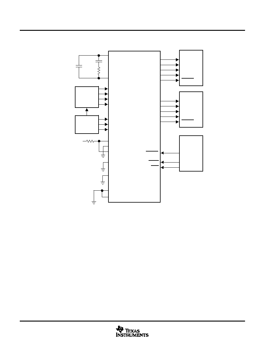
APPLICATION INFORMATION
Audio
Source
Clock
Generator
PLL_FLT_RET
PLL_FLT_OUT
DEM_SEL
DEM_EN
DBSPD
SDIN
LRCLK
SCLK
MCLK_IN
MOD0
MOD1
MOD2
M_S
TAS5110
H-Bridge
PWM_AP_L
PWM_AM_L
RESET
System
Controller
MUTE
PDN
3.3 V DIG
XTL_IN
C2
R1
C1
RESET
FTEST
TAS5012
VALID_L
TAS5110
H-Bridge
PWM_AP_R
PWM_AM_R
RESET
VALID_R
STEST
PWM_BP_L
PWM_BM_L
PWM_BP_R
PWM_BM_R
See application note SLAA117 for values.
TAS5012
SLES006A ≠ SEPTEMBER 2001 ≠ REVISED DECEMBER 2001
17
www.ti.com
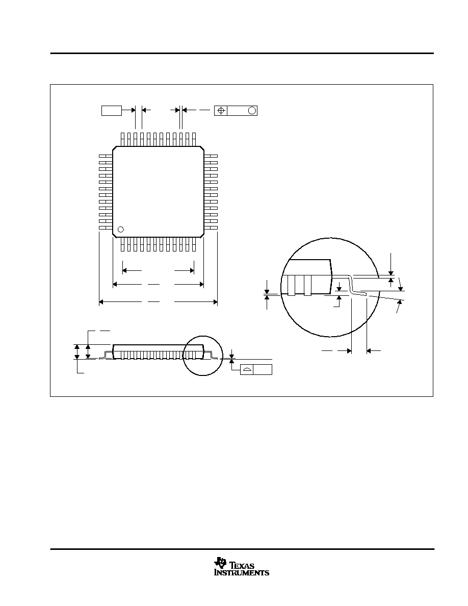
MECHANICAL DATA
PFB (S-PQFP-G48)
PLASTIC QUAD FLATPACK
4073176 / B 10/96
Gage Plane
0,13 NOM
0,25
0,45
0,75
Seating Plane
0,05 MIN
0,17
0,27
24
25
13
12
SQ
36
37
7,20
6,80
48
1
5,50 TYP
SQ
8,80
9,20
1,05
0,95
1,20 MAX
0,08
0,50
M
0,08
0
∞
≠ 7
∞
NOTES: A. All linear dimensions are in millimeters.
B. This drawing is subject to change without notice.
C. Falls within JEDEC MS-026

IMPORTANT NOTICE
Texas Instruments Incorporated and its subsidiaries (TI) reserve the right to make corrections, modifications,
enhancements, improvements, and other changes to its products and services at any time and to discontinue
any product or service without notice. Customers should obtain the latest relevant information before placing
orders and should verify that such information is current and complete. All products are sold subject to TI's terms
and conditions of sale supplied at the time of order acknowledgment.
TI warrants performance of its hardware products to the specifications applicable at the time of sale in
accordance with TI's standard warranty. Testing and other quality control techniques are used to the extent TI
deems necessary to support this warranty. Except where mandated by government requirements, testing of all
parameters of each product is not necessarily performed.
TI assumes no liability for applications assistance or customer product design. Customers are responsible for
their products and applications using TI components. To minimize the risks associated with customer products
and applications, customers should provide adequate design and operating safeguards.
TI does not warrant or represent that any license, either express or implied, is granted under any TI patent right,
copyright, mask work right, or other TI intellectual property right relating to any combination, machine, or process
in which TI products or services are used. Information published by TI regarding third≠party products or services
does not constitute a license from TI to use such products or services or a warranty or endorsement thereof.
Use of such information may require a license from a third party under the patents or other intellectual property
of the third party, or a license from TI under the patents or other intellectual property of TI.
Reproduction of information in TI data books or data sheets is permissible only if reproduction is without
alteration and is accompanied by all associated warranties, conditions, limitations, and notices. Reproduction
of this information with alteration is an unfair and deceptive business practice. TI is not responsible or liable for
such altered documentation.
Resale of TI products or services with statements different from or beyond the parameters stated by TI for that
product or service voids all express and any implied warranties for the associated TI product or service and
is an unfair and deceptive business practice. TI is not responsible or liable for any such statements.
Mailing Address:
Texas Instruments
Post Office Box 655303
Dallas, Texas 75265
Copyright
2001, Texas Instruments Incorporated