TAS5110
SLES028A ≠ MAY 2002 ≠ REVISED SEPTEMBER 2002
TRUE DIGITAL AUDIO AMPLIFIER
TAS5110 PWM POWER OUTPUT STAGE
1
www.ti.com
FEATURES
D
50-W RMS Power Into 6
at 10% THD
D
40-W RMS Power Into 6
at 0.1% THD
D
THD+N < 0.09% Typical (1-kHz Input Signal)
D
93-dB Dynamic Range (TDAA System)
D
Power Efficiency > 90% Into 6-
and 8-
Load
D
Low Profile, SMD 32-Pin PowerPAD
Package
D
Self-Protecting Design
D
3.3-V Digital Interface
D
EMI Compliant When Used With
Recommended System Design
APPLICATIONS
D
DVD Receiver
D
Home Theater
D
Mini/Micro Component Systems
D
Internet Music Appliance
D
Car Audio Amplifiers and Head Units
DESCRIPTION
The TAS5110 is a high-performance true digital audio
amplifier (TDAA) power stage, designed to drive 50 W
per channel. The TAS5110 incorporates TI's equibit
t
technology and is used in conjunction with a digital
audio PWM processor (TAS50xx) to deliver high-power,
true digital audio amplification. The efficiency of this
digital amplifier can be greater than 90%, reducing the
size of both the power supplies and heat sinks needed.
The TAS5110 accepts a mono PWM 3.3-V input and
controls the switching of an internal CMOS H-bridge.
When used with the TAS50xx PWM processor, system
performance of less than 0.09% THD is attainable.
Over-current protection, over-temperature, and
under-voltage protections are built into the TAS5110,
safeguarding the H-bridge and speakers against output
shorts, over-voltage conditions, and other fault
conditions that could damage the system.
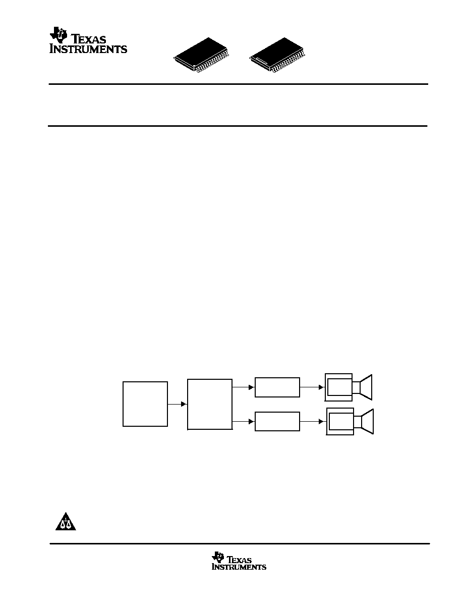
TYPICAL TDAA STEREO AUDIO SYSTEM
Digital Audio
∑
TAS3001
∑
DSP
∑
SPDIF
∑
1394
TAS50xx
L-C
Filter
L-C
Filter
Left
Right
TAS5110
∑
Volume
∑
EQ
∑
DRC
∑
Bass
∑
Treble
∑
Serial Audio Input Port
∑
Internal PLL
∑
PCM≠PWM Modulator
∑
Two H-Bridge Power Devices
TAS5110
PRODUCTION DATA information is current as of publication date.
Products conform to specifications per the terms of Texas Instruments
standard warranty. Production processing does not necessarily include
testing of all parameters.
PowerPAD and Equibit are trademarks of Texas Instruments.
Copyright
2002, Texas Instruments Incorporated
Please be aware that an important notice concerning availability, standard warranty, and use in critical applications of
Texas Instruments semiconductor products and disclaimers thereto appears at the end of this data sheet.

TAS5110
SLES028A ≠ MAY 2002 ≠ REVISED SEPTEMBER 2002
2
www.ti.com
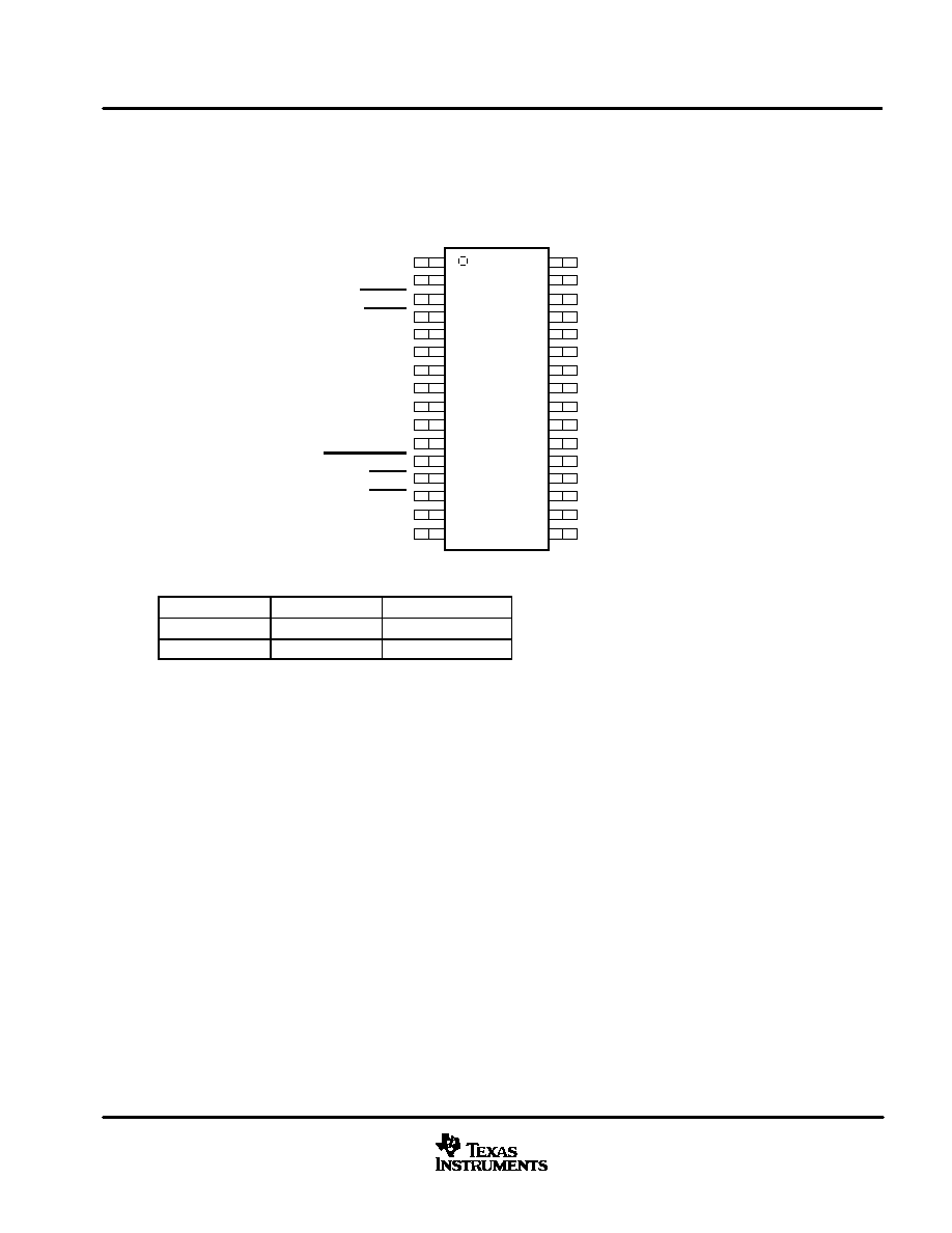
terminal assignments
The TAS5110 is offered in a thermally enhanced 32-pin HTSSOP surface-mount package (DAP). The DAP
package has the PowerPAD on the bottom.
1
2
3
4
5
6
7
8
9
10
11
12
13
14
15
16
32
31
30
29
28
27
26
25
24
23
22
21
20
19
18
17
PWM_AP
PWM_AM
ERR1
ERR0
SHUTDOWN
DVDD
DVSS
DVSS
DVSS
VRFILT
BIAS_A
BIAS_B
PWDN
RESET
PWM_BM
PWM_BP
PVDDA2
LDROUTA
BOOTSTRAPA
PVDDA1
PVDDA1
OUTPUTA
OUTPUTA
PVSS
PVSS
OUTPUTB
OUTPUTB
PVDDB1
PVDDB1
BOOTSTRAPB
LDROUTB
PVDDB2
DAP PACKAGE
(TOP VIEW)
ordering information
TC
PACKAGE
TAPE AND REEL
0
∞
C to 70
∞
C
TAS5110DAP
TAS5110DAPR
≠40
∞
C to 85
∞
C
TAS5110IDAP
TAS5110IDAPR
TAS5110
SLES028A ≠ MAY 2002 ≠ REVISED SEPTEMBER 2002
3
www.ti.com
terminal assignments
In addition to the 32-pin HTSSOP DAP package, the TAS5110 is offered in a thermally enhanced 32-pin TSSOP
surface-mount package (DAD). The DAD package has the PowerPAD on top.
1
2
3
4
5
6
7
8
9
10
11
12
13
14
15
16
32
31
30
29
28
27
26
25
24
23
22
21
20
19
18
17
PWM_BP
PWM_BM
RESET
PWDN
BIAS_B
BIAS_A
VRFILT
DVSS
DVSS
DVSS
DVDD
SHUTDOWN
ERR0
ERR1
PWM_AM
PWM_AP
PVDDB2
LDROUTB
BOOTSTRAPB
PVDDB1
PVDDB1
OUTPUTB
OUTPUTB
PVSS
PVSS
OUTPUTA
OUTPUTA
PVDDA1
PVDDA1
BOOTSTRAPA
LDROUTA
PVDDA2
DAD PACKAGE
(TOP VIEW)
ordering information
TC
PACKAGE
TAPE AND REEL
0
∞
C to 70
∞
C
TAS5110DAD
TAS5110DADR
≠40
∞
C to 85
∞
C
TAS5110IDAD
TAS5110IDADR
references
TAS5000 Digital Audio PWM Processor data manual ≠ TI Literature Number SLAS270
TAS5001 Digital Audio PWM Processor data manual ≠ TI Literature Number SLES009
TAS5010 Digital Audio PWM Processor data manual ≠ TI Literature Number SLAS328
TAS5012 Digital Audio PWM Processor data manual ≠ TI Literature Number SLES006
Digital Audio Measurements ≠ TI literature number SLAA114
PowerPAD Thermally Enhanced Package ≠ TI literature number SLMA002
TAS5110
SLES028A ≠ MAY 2002 ≠ REVISED SEPTEMBER 2002
4
www.ti.com
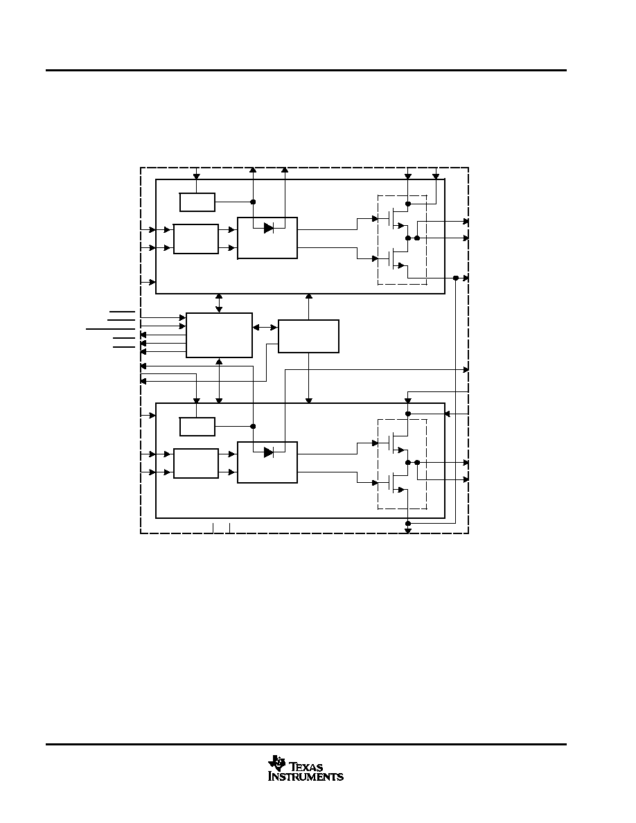
functional block diagram
Boot Strap
Gate Drive
DIFF
RCVR
LDR
Boot Strap
Gate Drive
DIFF
RCVR
LDR
Control/Sense
Circuit
Bandgap
Reference
1/2 H-Bridge
1/2 H-Bridge
OUTPUTA
OUTPUTA
PVSS
BOOTSTRAPB
PVDDB1
PVDDB1
OUTPUTB
OUTPUTB
DVDD
DVSS
PVSS
PWM_AP
PWM_AM
PWDN
RESET
SHUTDOWN
ERR1
ERR0
LDROUTB
VRFILT
PVDDB2
PWM_BM
PWM_BP
PVDDA2
LDROUT
A
BOOTSTRAP
A
PVDDA1
PVDDA1
BIAS_A
BIAS_B
TAS5110
SLES028A ≠ MAY 2002 ≠ REVISED SEPTEMBER 2002
5
www.ti.com
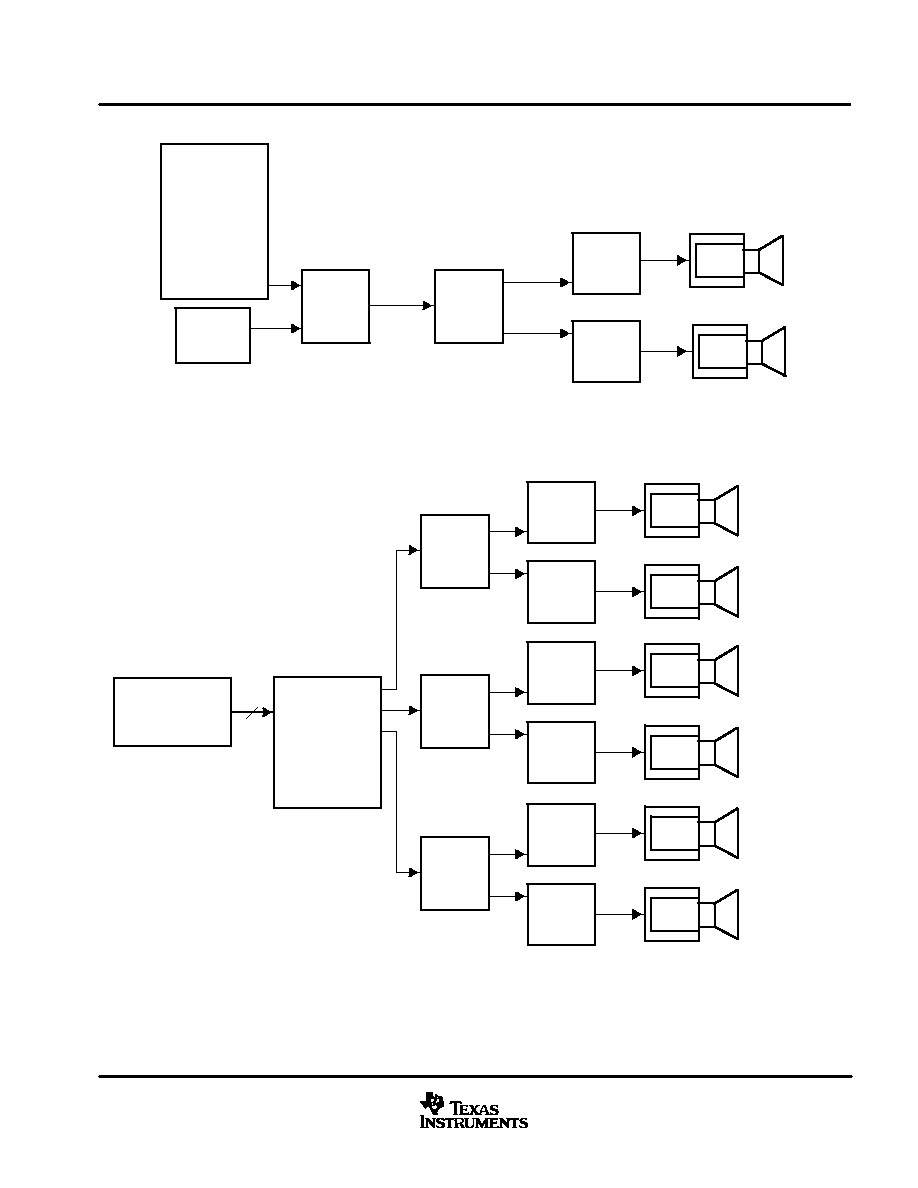
suggested system block diagrams
∑
USB
∑
IEEE 1394
∑
SPDIF
∑
ADC
∑
Automotive
MOST
Network
Digital Audio
TAS30xx
IIC
Audio
Control
TAS50xx
TAS5110
Left
Right
∑
Digital Parametric EQ
∑
Volume
∑
DRC
∑
Bass
∑
Treble
∑
Serial Audio Input Port
∑
Internal PLL
∑
Two H-Bridges
TAS5110
L-C
Filter
L-C
Filter
Figure 1. System #1: Stereo Configuration With a TAS3001 Digital Audio Processor
TI DSP
∑
Dolby AC-3
∑
DTS
∑
Volume
∑
EQ
∑
DRC
∑
Bass
∑
Treble
Home Theater
DVD 6-Channel
Encoded Digital
Audio Source
TAS50xx
TAS5110
CH1
CH2
TAS50xx
CH3
CH4
TAS50xx
CH5
CH6
6
TAS5110
TAS5110
TAS5110
TAS5110
TAS5110
Left
Right
Surround Left
Surround Right
Center
Subwoofer
L-C
Filter
L-C
Filter
L-C
Filter
L-C
Filter
L-C
Filter
L-C
Filter
Figure 2. System #3: 6-Channel Audio Playback

TAS5110
SLES028A ≠ MAY 2002 ≠ REVISED SEPTEMBER 2002
6
www.ti.com
Terminal Functions
TERMINAL
NAME
DAP
NO.
DAD
NO.
I/O
DESCRIPTION
BIAS_A
11
6
I
Connect external resistor to DVSS.
BIAS_B
12
5
I
Connect external resistor to DVSS.
BOOTSTRAPA
30
19
O
Bootstrap capacitor pin for H-bridge A
BOOTSTRAPB
19
30
O
Bootstrap capacitor pin for H-bridge B
DVDD
6
11
I
3.3-V digital voltage supply for logic
DVSS
7, 8, 9
8, 9,
10
I
Digital ground for logic is internally connected to PVSS. All three pins must be tied
together but not connected externally to PVSS. See Figure 5.
ERR1
3
14
O
Error/warning report indicator. This output is open drain with internal pullup resistor.
ERR0
4
13
O
Error/warning report indicator. This output is open drain with internal pullup resistor.
LDROUTA
31
18
O
Low voltage drop-out regulator output A (not to be used to supply current to external
circuitry)
LDROUTB
18
31
O
Low voltage drop-out regulator output B (not to be used to supply current to external
circuitry)
OUTPUTA
26, 27
22, 23
O
H-bridge output A
OUTPUTB
22, 23
26, 27
O
H-bridge output B
PVDDA1
28, 29
20, 21
I
High voltage power supply, H-bridge A
PVDDA2
32
17
I
High voltage power supply for low-dropout voltage regulator A-side
PVDDB1
20, 21
28, 29
I
High voltage power supply, H-bridge B
PVDDB2
17
32
I
High voltage power supply for low-dropout voltage regulator B-side
PVSS
24, 25
24, 25
I
High voltage power supply ground
PWDN
13
4
I
Power down = 0, normal mode = 1
PWM_AM
2
15
I
PWM input A(≠)
PWM_AP
1
16
I
PWM input A(+)
PWM_BP
16
1
I
PWM input B(+)
PWM_BM
15
2
I
PWM input B(≠)
RESET
14
3
I
Reset and mute mode = 0, normal mode = 1, when in reset mode, H-bridge MOSFETs are
in low-low output state. Asserting the RESET signal low causes all fault conditions to be
cleared.
SHUTDOWN
5
12
O
Device is in shutdown due to fault condition, normal mode = 1, shutdown = 0, when
device is in shutdown mode the H-bridge MOSFETs are in low-low output state. The
latched output can be cleared by asserting the RESET signal. This output is open drain
with internal pullup resistor.
VRFILT
10
7
O
A filter capacitor must be added between VRFILT and DVSS pins.
NOTE: The four PWM inputs: PWM_AP, PWM_AM, PWM_BP, and PWM_BM must always be connected to the TAS50xx output pins, and never
left floating. Floating PWM input pins causes an illegal PWM input state signal to be asserted.
Dual pins: OUTPUTA, OUTPUTB, PVDDA1, and PVDDB1 must have both pins connected externally to the same point on the circuit board,
respectively. Both PVSS pins must also be connected together externally. These multiple pins are for the high-current DMOS output
devices. Failure to connect all the multiple pins to the same respective node results in excessive current flow in the internal bond wires
and can cause the device to fail. All electrical characteristics are specified and measured with all of the multiple pins connected to the same
node, respectively.

TAS5110
SLES028A ≠ MAY 2002 ≠ REVISED SEPTEMBER 2002
7
www.ti.com
functional description
PWM H-bridge state control
The digital interface control signals consists of PWM_AP, PWM_AM, PWM_BP, and PWM_BM. These signals
are a complementary differential signal format for the A-side half-bridge and the B-side half-bridge.
bootstrapped gate drive
The TAS5110 includes two dedicated bootstrapped power supplies. A bootstrap capacitor is connected
between the individual bootstrap pin and the associated output. For example, a capacitor is connected between
the BOOTSTRAPA pin and OUTPUTA pin, and another capacitor is connected between the BOOTSTRAPB
pin and the OUTPUTB pin. The bootstrap power supply minimizes the number of high voltage power supply
levels externally supplied to the system while providing a low-noise supply level for driving the high-side
N-channel DMOS transistors.
low-dropout voltage regulator
Two on-chip low-dropout voltage regulators (LDO) are provided to minimize the number of external power
supplies needed for the system. These voltage regulators are for internal circuits only and cannot be used for
external circuitry. Each LDO is dedicated to a half-bridge and its gate driver. An LDO output capacitor is
connected between the individual LDO output pin and the associated output return. For example, a capacitor
is connected between the LDROUTA pin and PVSS pin, and another capacitor is connected between the
LDROUTB pin and PVSS pin.
high-current H-bridge output stage
The positive outputs of the H-bridge are the two OUTPUTA pins. The negative outputs of the H-bridge are the
two OUTPUTB pins. The logic for the input command to H-bridge outputs is described in the H-bridge output
mapping section below. When the TAS5110 is in the normal mode, as seen in the H-bridge output mapping
tables, the outputs are decoded from the inputs. However, the TAS5110 is immediately shut down if any of the
following error conditions occur: over-current, over-temperature, low regulator output voltage, or an illegal PWM
input state is applied. For these conditions, the outputs are set to the appropriate disabled state as specified
in the H-bridge output mapping section, and the SHUTDOWN pin is set low.
H-bridge output mapping
The A-side half-bridge output is designed to the following truth table:
INPUTS
OUTPUTS
DESCRIPTION
RESET
PWDN
PWM_AP
PWM_AM
SHUTDOWN
OUTPUTA
DESCRIPTION
X
X
X
X
0
0 or Hi-Z
Shutdown
X
0
X
X
1
Hi-Z
Powerdown
0
1
X
X
1
0
Reset
1
1
0
0
0
0
Shutdown
1
1
0
1
1
0
Normal
1
1
1
0
1
1
Normal
1
1
1
1
0
0
Shutdown
Output is 0 for low voltage, over temperature, and illegal input. Hi-Z is for over current.
TAS5110
SLES028A ≠ MAY 2002 ≠ REVISED SEPTEMBER 2002
8
www.ti.com
H-bridge output mapping (continued)
The B-side half-bridge output is designed to the following truth table:
INPUTS
OUTPUTS
DESCRIPTION
RESET
PWDN
PWM_BP
PWM_BM
SHUTDOWN
OUTPUTB
DESCRIPTION
X
X
X
X
0
0 or Hi-Z
Shutdown
X
0
X
X
1
Hi-Z
Powerdown
0
1
X
X
1
0
Reset
1
1
0
0
0
0
Shutdown
1
1
0
1
1
0
Normal
1
1
1
0
1
1
Normal
1
1
1
1
0
0
Shutdown
Output is 0 for low voltage, over temperature, or illegal input. Hi-Z is for over current.
control/sense circuitry
The control/sense circuitry consists of the following 3.3-V logic level pins: PWDN, RESET, ERR0, ERR1, and
SHUTDOWN. The active-low PWDN input pin powers down all internal circuitry and forces the H-bridge outputs
to the Hi-Z state. When the PWDN pin is low, the open drain ERR0, ERR1, and SHUTDOWN pins are also
disabled so that their outputs can be pulled high. The active-low RESET input pin forces the H-bridge outputs
to the low-low state and resets the over-current shutdown latch. The PWDN pin overrides the RESET pin. The
ERR0, ERR1, and SHUTDOWN outputs indicate the following conditions in the TAS5110 as shown in the table
below. These three outputs are open-drain connections with internal pullup resistors so that wire-ORed
connections can be made by the user with other external control devices. The short-circuit protect error
condition latches the TAS5110 in this shutdown state and forces the H-bridge outputs to the Hi-Z state until the
device is reset by means of the RESET pin. The illegal PWM input state, over-temperature, and low regulator
voltage error conditions does not latch the device in the shutdown condition. Instead the H-bridge outputs are
forced to the low-low state and the TAS5110 returns to normal operation as soon as the error condition ends.
Loss of clocking PWM signal is also considered an illegal PWM input state.
SHUTDOWN
ERR1
ERR0
FUNCTION
OUTPUTA
OUTPUTB
0
0
0
Illegal PWM input state
Low
Low
0
0
1
Short circuit protect (latch)
Hi-Z
Hi-Z
0
1
0
Over temperature protect
Low
Low
0
1
1
Low regulator voltage protect
Low
Low
1
0
0
Reserved
--
--
1
0
1
Reserved
--
--
1
1
0
High temperature ≠ warning
Normal
Normal
1
1
1
Normal operation
Normal
Normal

TAS5110
SLES028A ≠ MAY 2002 ≠ REVISED SEPTEMBER 2002
9
www.ti.com
device operation
power sequences
system power-up/power-down sequencing
The recommended power-up/power-down sequence is shown in Figure 3. For proper operation the RESET
signal should be kept low when both DVDD and output power (PVDDA1, PVDDA2, PVDDB1, and PVDDB2)
are being applied. The RESET signal should remain low for at least 1 ms after output power is applied.
> 1 ms
DVDD
PWDN
PVDDA2
PVDDB2
RESET
> 1 ms
> 100
µ
s
> 100
µ
s
PVDDA1
PVDDB1
For most applications, it is recommended that the PWDN pin be connected directly to the DVDD pin.
Figure 3. Power-Up/Power-Down Sequence
RESET function
The device is put into a reset condition when the (active low) RESET signal is asserted. While in the reset state,
the input H-bridge control signals consisting of PWM_AP, PWM_AM, PWM_BP, and PWM_BM are ignored, and
the H-bridge MOSFETs are placed in a state where OUTPUTA and OUTPUTB are both low. Asserting the
RESET signal low also causes the short circuit protection latch to be reset. The RESET signal is normally
connected to the VALID signal from the TAS50xx.
reinitialization sequence
Proper initial conditions for this device include asserting the RESET signal until the reset operation has
completed (1 ms). Additionally, when using this device with the TAS50xx controller, this function can be
accomplished by asserting the reset pin on the TAS50xx during the reset sequence (see Figure 3).
audio application considerations
optimal power transfer for H-bridge
The TAS5110 is a power H-bridge that is designed to deliver a maximum of 50 W RMS into a 6-
load. In order
to achieve 50 W into 6
, the system designer must provide an adequate thermal design. See the Thermal
Methodology for the 32-Pin DAD Package 50 W, 6-
Test and the Thermal Methodology for the 32-Pin DAP
Package 50 W, 6-
sections for a discussion of possible thermal solutions. Careful attention must be given to
the value of the high-voltage power supply level for a given load resistance. See recommended operating
conditions. See the Maximum Available Power at Common Load Impedances for Both DAP and DAD Packages
section.

TAS5110
SLES028A ≠ MAY 2002 ≠ REVISED SEPTEMBER 2002
10
www.ti.com
audio application considerations (continued)
reconstruction output filter
An output reconstruction filter is required between the H-bridge outputs and the loudspeaker load. This second
order low-pass filter passes the audio information to the loudspeaker, while filtering out the high frequency
out-of-band information contained in the H-bridge output PWM pulses. The values of the L and C components
selected are dependent on the loudspeaker load impedance.
fault indicator usage
The TAS5110 is a self-protecting device that provides device fault reporting, including over-temperature protect,
under-voltage lockout (low-regulator voltage), and short circuit protection. The short circuit protection protects
against short circuits that may occur at the loudspeaker load when configured. The TAS5110 is not
recommended for driving loads less than 6
,
since the internal current limit protection might be activated.
An under-voltage lockout signal occurs when an insufficient voltage level is present on the LDROUTA or
LDROUTB pins. During this condition gate drive levels are not sufficient for driving the power MOSFETs. Normal
operation is resumed when the minimum proper LDROUTA or LDROUTB level is obtained and the low regulator
voltage protect signal is de-asserted. See the control/sense circuitry section for error and warning conditions.
A high temperature warning signal is asserted on pin ERR0 when the device temperature exceeds 125
∞
C
typical.
If the internal device temperature exceeds 150
∞
C typical, the over temperature protect signal is asserted and
the TAS5110 is shut down. The device re-enables once the temperature drops to 125
∞
C typical. See the
control/sense circuitry section for error and warning conditions.
Detection of an illegal PWM input state or the loss of a clocking PWM input signal causes an illegal PWM input
state signal to be asserted on the ERR1and ERR0 pins and sets the SHUTDOWN pin to the low state.
absolute maximum ratings over operating free-air temperature (unless otherwise noted)
DC supply voltage range: DVDD to DVSS
≠0.3 V to 4.2 V
. . . . . . . . . . . . . . . . . . . . . . . . . . . . . . . . . . . . . . . . . . . . . . . . .
PWM_AP, PWM_AM, PWM_BP, PWM_BM
≠0.3 V to DVDD + 0.3 V
. . . . . . . . . . . . . . . . .
RESET, PWDN
≠0.3 V to DVDD + 0.3 V
. . . . . . . . . . . . . . . . . . . . . . . . . . . . . . . . . . . . . . . .
PVDDA1 to PVSS, PVDDB1 to PVSS
≠0.3 V to 28 V
. . . . . . . . . . . . . . . . . . . . . . . . . . . . .
PVDDA2 to PVSS, PVDDB2 to PVSS
≠0.3 V to 27 V
. . . . . . . . . . . . . . . . . . . . . . . . . . . . .
Output DMOS drain-to-source breakdown voltage
28 V
. . . . . . . . . . . . . . . . . . . . . . . . . . . . . . . . . . . . . . . . . . . . . . . . . . .
Operating junction temperature range, T
J
≠40
∞
C to 150
∞
C
. . . . . . . . . . . . . . . . . . . . . . . . . . . . . . . . . . . . . . . . . . . . . . .
Storage temperature range, T
stg
≠65
∞
C to 150
∞
C
. . . . . . . . . . . . . . . . . . . . . . . . . . . . . . . . . . . . . . . . . . . . . . . . . . . . . . . .
Lead temperature 1,6 mm (1/16 inch) from case for 10 seconds)
260
∞
C
. . . . . . . . . . . . . . . . . . . . . . . . . . . . . . . . . . . .
Stresses beyond those listed under "absolute maximum ratings" may cause permanent damage to the device. These are stress ratings only, and
functional operation of the device at these or any other conditions beyond those indicated under "recommended operating conditions" is not
implied. Exposure to absolute-maximum-rated conditions for extended periods may affect device reliability.
TAS5110
SLES028A ≠ MAY 2002 ≠ REVISED SEPTEMBER 2002
11
www.ti.com
recommended operating conditions (maximum output power = 50 W (RMS), T
J
= 25
∞
C)
thermal data
PARAMETER
MIN
NOM
MAX
UNIT
Shutdown junction temperature, TJ(SD)
150
∞
C
Warning junction temperature, TJ(W)
125
∞
C
Operating temperature TC
Commercial
0
25
70
∞
C
Operating temperature, TC
Industrial
≠40
25
85
∞
C
Thermal resistance junction-to-case,
jc
}
2 oz trace and copper pad without solder
1.6
∞
C/W
Thermal resistance junction-to-ambient,
ja
}
2 oz. trace and copper pad without solder
44.3
∞
C/W
One of the most influential components on the thermal performance of a package is board design. In order to take full advantage of the heat
dissipating abilities of the PowerPAD packages, a board must be used that acts similar to a heat sink and allows for the use of the exposed (and
solderable), deep downset pad. See Appendix A of the PowerPAD Thermally Enhanced Package application note, TI literature number
SLMA002.
For both DAD and DAP packages.
R
L
= 6
to 8
PARAMETER
MIN
NOM
MAX
UNIT
Digital
DVDD to DVSS
3
3.3
3.6
V
PVDDA2 to PVSS
16.5
22
26.5
Supply voltage
Regulator
PVDDB2 to PVSS
16.5
22
26.5
V
y
g
Regulator
PVDDA2 to PVSS
w
10.5
16.5
V
PVDDB2 to PVSS
w
10.5
16.5
ß Connect LDROUTA to PVDDA2 and connect LDROUTB to PVDDB2. Under this condition, the H-bridge forward on-state resistance is increased.
This increases internal power dissipation. Maximum output power may need to be reduced to meet thermal conditions.
maximum available power at common load impedances for both DAP and DAD packages unclipped (0 dB)
level, test conditions described in the Thermal Methodology for the 32-Pin DAD Package 50 W, 6-
Test and
Thermal Methodology for the 32-Pin DAP Package 50 W, 6-
Test sections
LOAD IMPEDANCE (
)
PVDAA1/PVDDB1 (VDC)
APPROXIMATE MAX OUTPUT POW-
THD+N AT MAX POWER AND 1 kHz
LOAD IMPEDANCE (
)
PVDAA1/PVDDB1 (VDC)
APPROXIMATE MAX OUTPUT POW-
ER (W)
THD+N AT MAX POWER AND 1 kHz
INPUT∂
6
27
50
< 10%
6
27
43
< 0.09%
8
27
34
< 0.09%
∂ Dependent on board design and component selection.
static digital specifications
RESET, PWDN, PWM_AP, PWM_AM, PWM_BP, PWM_BM, T
J
= 25
∞
C, DVDD = 3.3 V
PARAMETERS
MIN
MAX
UNIT
High-level input voltage, VIH
2
V
Low-level input voltage, VIL
0.8
V
Input leakage current
≠10
10
µ
A
ERR0, ERR1, SHUTDOWN, (open drain with internal pullup resistor) T
J
= 25
∞
C, DVDD = 3.3 V)
PARAMETERS
MIN
MAX
UNIT
Internal pullup resistors from SHUTDOWN, ERR0, ERR1 to DVDD
15
k
Low-level output voltage (IO = 4 mA), VOL
0.4
V

TAS5110
SLES028A ≠ MAY 2002 ≠ REVISED SEPTEMBER 2002
12
www.ti.com
electrical characteristics
supply, T
J
= 25
∞
C (F
switching
= 384 kHz, OUTPUTA and OUTPUTB not connected, DVDD = 3.3 V,
PVDDA1 = 25 V, PVDDB1 = 25 V, PVDDA2 = 22 V, PVDDB2 = 22 V, 50% input duty cycle)
PARAMETER
TYP
MAX
UNIT
DVDD
Operating
2
mA
DVDD
PWDN = 0
500
µ
A
Supply current
PVDDA1
Operating
6.3
mA
Supply current
PVDDA1
PVDDB1
PWDN = 0
25
µ
A
PVDDA2
Operating
6.5
mA
PVDDA2
PVDDB2
PWDN = 0
250
µ
A
13-k
resistor from BIAS_A (pin 11) to DVSS and 13-k
resistor from BIAS_B (pin 12) to DVSS.
H-Bridge transistors, PVDDA2 = PVDDB2 = 22 V, DVDD = 3.3 V, T
J
= 25
∞
C (unless otherwise noted)
PARAMETER
TEST CONDITIONS
MIN
TYP
MAX
UNIT
Drain-to-source breakdown voltage
ID = 1 mA, PWDN = 0, Hi-Z state
28
V
Forward on-state resistance, low-side drivers
OUTPUTA and OUTPUTB to PVSS
ISINK = 2.5 A,
See Notes 1, 2, and 3,
PWM_AP = PWM_BP = 0,
PWM_AM = PWM_BM = 1
0.2
0.24
Forward on-state resistance, high-side drivers
PVDDA1 to OUTPUTA, PVDDB1 to OUTPUTB
ISOURCE = 2.5 A,
See Notes 1, 2, and 4,
PWM_AP = PWM_BP = 1,
PWM_AM = PWM_BM = 0
0.2
0.24
On-state resistance matching low-side drivers
98%
On-state resistance matching high-side drivers
98%
NOTES:
1. Test time should be < 1 ms to avoid temperature change.
2. These parameters are measured with voltage-sensing contacts separate from the current-carrying contacts.
3. Connect PVDDA2 and PVDDB2 to a 22-V power supply with respect to PVSS. LDROUTA, LDROUTB, BOOTSTRAPA, and
BOOTSTRAPB pins open.
4. Connect PVDDA2 to 22-V power supply with respect to PVSS. LDROUTA, LDROUTB, BOOTSTRAPA, and BOOTSTRAPB
capacitors are connected respectively. Clock PWM inputs to allow bootstrap capacitors to charge. 93≠99% modulation must be used
on PWM_AP, PWM_AM, PWM_BP, and PWM_BM inputs to prevent the activity detector from shutting down the device during this
measurement. Note that Fswitching = 384 kHz.
electrical characteristics, voltage regulator, T
J
= 25
∞
C (unless otherwise noted)
PARAMETER
TEST CONDITIONS
MIN
TYP
MAX
UNIT
Output voltage (LDROUTA, LDROUTB)
IO = 5 mA, PVDDA2 = PVDDB2 = 18 V to 27 V,
See Note 5, DVDD = 3.3 V
14.5
15.3
16
V
NOTE 5: These voltage regulators are for internal gate drive circuits only and are not to be used under any circumstances to supply current to
external circuity.

TAS5110
SLES028A ≠ MAY 2002 ≠ REVISED SEPTEMBER 2002
13
www.ti.com
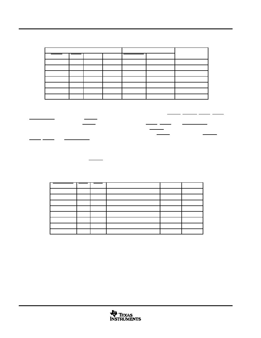
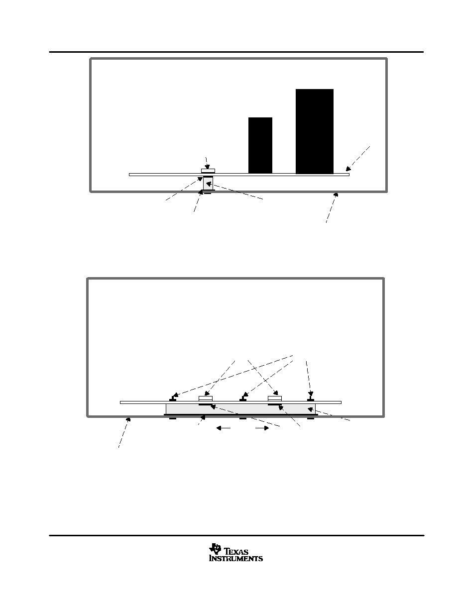
r(on) ≠ On-State Resistance ≠
0
20
40
60
80
100
120
140
160
0.15
0.20
0.25
0.30
0.35
0.40
T
J
≠
Junction T
emperature
≠
∞
C
JUNCTION TEMPERATURE
vs
ON-STATE RESISTANCE
Figure 4. Temperature vs On-State Resistance
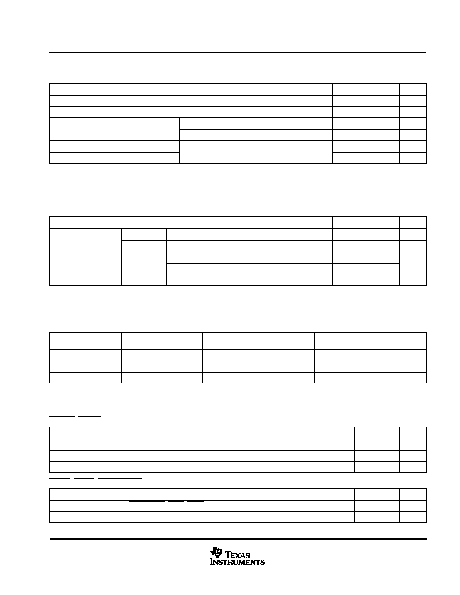
APPLICATION INFORMATION
TAS5110 (DAP Package)
1
2
3
4
5
6
7
8
9
10
11
12
13
14
15
16
17
18
19
20
21
22
23
24
25
26
27
28
29
30
31
32
Snubber
Circuit
Error
Reporting
Snubber
Circuit
_
+
dc
PWM_AP
PWM_AM
ERR1
ERR0
SHUTDOWN
DVDD
DVSS
DVSS
DVSS
VRFILT
BIAS_A
BIAS_B
PWDN
RESET
PWM_BM
PWM_BP
PVDDA2
LDROUTA
BOOTSTRAPA
PVDDA1
PVDDA1
OUTPUTA
OUTPUTA
PVSS
PVSS
OUTPUTB
OUTPUTB
PVDDB1
PVDDB1
BOOTSTRAPB
LDROUTB
PVDDB2
L1
L2
C1
R1
R2
C2
C3
C4
C5
C6
3.3 V
RESET
PWM_M_L
PWM_P_L
VALID
TAS50xx
C7
22 V
22 V
Figure 5. Typical TAS5110 Application (One Channel Shown)
TAS5110
SLES028A ≠ MAY 2002 ≠ REVISED SEPTEMBER 2002
14
www.ti.com
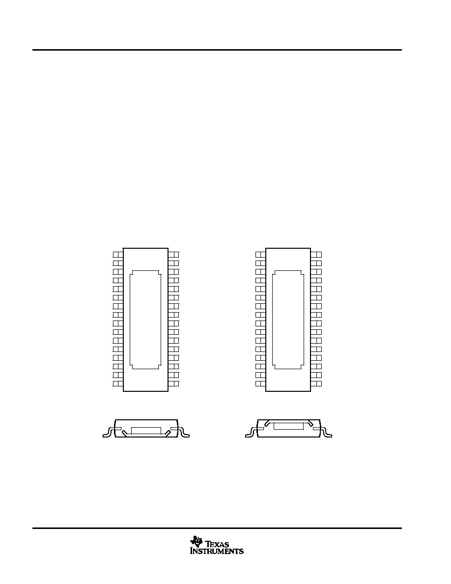
THERMAL INFORMATION
The thermally enhanced DAP package is based on the 32-pin HTSSOP, but includes a thermal pad (see
Figure 6) to provide an effective thermal contact between the IC and the PCB.
Traditionally, surface mount and power have been mutually exclusive terms. A variety of scaled-down TO-220
type packages have leads formed as gull wings to make them applicable for surface-mount applications. These
packages, however, have two shortcomings: they do not address the low profile requirements (<2 mm) of many
of today's advanced systems, and they do not offer a terminal-count high enough to accommodate increasing
integration. On the other hand, traditional low-power surface-mount packages require power-dissipation
derating that severely limits the usable range of many high-performance analog circuits.
The PowerPAD package (thermally enhanced HTSSOP) combines fine-pitch surface-mount technology with
thermal performance comparable to much larger power packages.
The PowerPAD package is designed to optimize the heat transfer to the PCB. Because of the very small size
and limited mass of a HTSSOP package, thermal enhancement is achieved by improving the thermal
conduction paths that remove heat from the component. The thermal pad is formed using a patented lead-frame
design and manufacturing technique to provide a direct connection to the heat-generating IC. When this pad
is soldered or otherwise thermally coupled to an external heat dissipater, high power dissipation in the ultrathin,
fine-pitch, surface-mount package can be reliably achieved. See the dissipation derating table.
DIE
Thermal
Pad
End View DAP
Bottom View DAP
DIE
End View DAD
Thermal
Pad
Top View DAD
DAP Package
DAD Package
Figure 6. Views of Thermally Enhanced DAP Package
TAS5110
SLES028A ≠ MAY 2002 ≠ REVISED SEPTEMBER 2002
15
www.ti.com
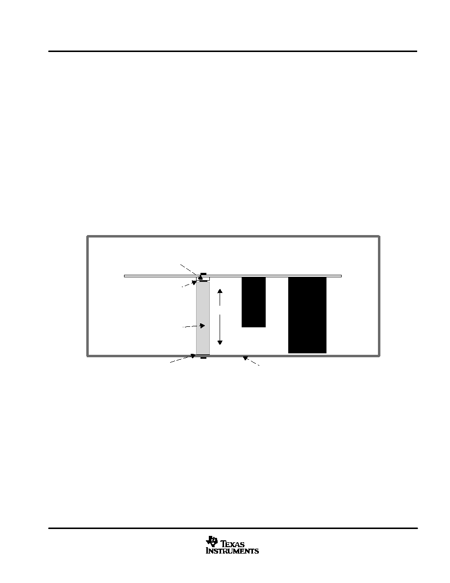
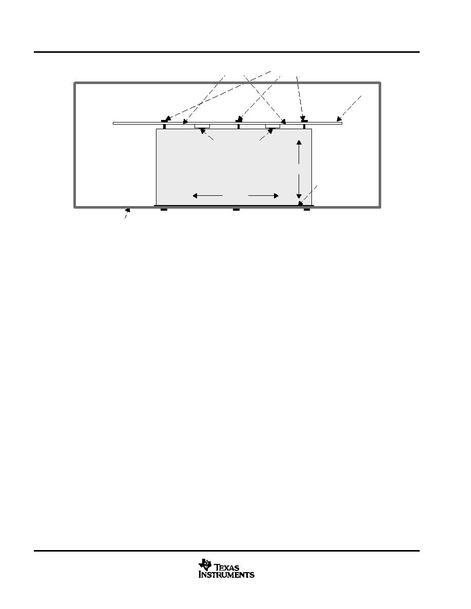
Thermal Methodology for the 32-Pin DAD Package 50 W, 6-
Test
The thermal test for the DAD part (e.g., thermal pad oriented away from the board) was conducted as shown
in Figure 7 and Figure 8. The cooling approach was to attach a heat sink to the thermal pad and conduct the
heat to ambient air.
Since the approach was to use a chassis below the board, it was inverted and a spacer bar used to connect
the pads thermally to the heat sink. The bar was made high enough that the components on the board were
clear of the chassis.
The pad-to-spacer thermal resistance was about 3.2
_
C/W with the thermal compound indicated.
The chassis provided the only heat sink to air and was chosen as representative of a possible cooling approach.
A closed plastic top and insulating front and back panels ensured that only the bottom and sides of the U shaped
chassis contributed to cooling. The chassis was spaced 0.25 inch from the table to simulate a normal chassis
configuration. The thermal pad does not need to be isolated from ground. (Any heat sink with a thermal
resistance to air of 3.9
_
C/W or lower also works.) In this test, the exposed chassis reached long-term equilibrium
temperatures above 50
_
C, so the approach would have to be modified for touch temperature consideration. The
chassis temperature after 10 minutes of 50 W into 6
was below 50
_
C.
The test ran for three hours with 2 x 50 W RMS at 1 kHz into a 6-
resistive load at an ambient lab temperature
of 23
_
C. No audio or thermal problems were encountered during that time.
ŒŒŒŒŒŒŒŒŒŒŒŒŒŒŒŒŒŒŒŒ
œœ
32 DAD Package
Wakefield Type 126
Thermal Compound
(3.2
∞
C/W)
Aluminum Space Bar
(1/4 in Thick)
(2.44
∞
C/W)
Stereo Amplifier
Board
Wakefield Type 126
Thermal Compound
(0.169
∞
C/W)
1.25 in
Aluminum Chassis 7.2 in x 1 in x 0.1 in Thick
Sides of U-Shaped Chassis Are 1.25 in High
(3.9
∞
C/W)
Insulating
Back Panel
Insulating
Front Panel
Plastic Top Cover
Figure 7. 32-Pin DAD Package Cross-Sectional View (Side)
TAS5110
SLES028A ≠ MAY 2002 ≠ REVISED SEPTEMBER 2002
16
www.ti.com
ŒŒŒŒŒŒŒŒŒŒŒŒŒŒŒŒŒŒŒŒ
œœ
œœ
Aluminum Chassis 7.2 in x 1 in x 0.1 in Thick Sides of U-Shaped
Chassis Are 1.25 in High (3.9
∞
C/W)
Wakefield Type 126
Thermal Compound
(0.169
∞
C/W)
1.25 in
Aluminum Space Bar (1/4 in Thick)
(0.558
∞
C/W)
32 DAD Packages
(1.6
∞
C/W)
2.33 in
Stereo Amplifier Board
4-40 Machine Screws With
Star Washers
Plastic Top and Insulating
Front and Back Panels
1 mm
Wakefield Type 126
Thermal Compound
(3.2
∞
C/W)
Figure 8. 32-Pin DAD Package Cross-Sectional View (Front)
Thermal Methodology for the 32-Pin DAP Package 50 W, 6-
Test
The thermal test for the DAP part (e.g., thermal pad soldered to the board) was conducted as shown in Figure 9
and Figure 10. The cooling approach was to conduct the dissipated heat into the via pad on the board, through
the vias in the board, and into a heat sink.
The lower via pad area, slightly larger than the IC pad itself, was exposed with a window in the solder resist on
the bottom surface of the board. It was not coated with solder during the board construction to maintain a flat
surface. In production, this could be accomplished with a peelable solder mask.
A spacer bar was used to keep the through-hole leads from shorting to the chassis. The thermal compound
indicated yielded a pad-to-spacer thermal resistance of about 3.2
_
C/W.
The chassis provided the only heat sink to air and was chosen as representative of a possible cooling approach.
A plastic top and insulating front and back panels were used to ensure that only the bottom and sides of the U
shaped chassis contributed to cooling. The chassis was spaced 0.25 inch from the table to simulate a normal
chassis configuration. (Any heat sink with a thermal resistance to air of 3.9
_
C/W or lower also works.) In this
test, the exposed chassis reached long-term equilibrium temperatures above 50
_
C, so the approach would
have to be modified for touch temperature consideration. The chassis temperature after 10 minutes of 50 W
into 6
was below 50
_
C.
The test ran for three hours with 2 x 50 W RMS at 1 kHz into a 6-
resistive load at an ambient lab temperature
of 23
_
C. No audio quality or thermal problems were encountered during that time.
TAS5110
SLES028A ≠ MAY 2002 ≠ REVISED SEPTEMBER 2002
17
www.ti.com
ŒŒŒŒŒŒŒŒŒŒŒŒŒŒŒŒŒŒŒŒ
œœ
œœ
Aluminum Chassis 7.2 in x 1 in x 0.1 in Thick
Sides of U-Shaped Chassis Are 1.25 in High (3.9
∞
C/W)
32 DAP Package
1/4 in x 1/4 in x 2.33 in
Aluminum Space Bar
(0.09
∞
C/W)
Insulating
Back Panel
Insulating
Front Panel
1 mm
Stereo Amplifier Board
Wakefield Type 126
Thermal Compound
Under Via Pads
(4.3
∞
C/W)
Wakefield Type 126
Thermal Compound
(0.1
∞
C/W)
Figure 9. 32-Pin DAP Package Cross-Sectional View (Side)
ŒŒŒŒŒŒŒŒŒŒŒŒŒŒŒŒŒŒŒŒ
œœ
ÃÃ
ÃÃ
œœ
ÃÃ
ÃÃ
Aluminum Chassis 7.2 in x 1 in x 0.1 in Thick
Sides of U-Shaped Chassis Are 1.25 in High
(3.9
∞
C/W)
2.33 in
4-40 Machine Screws With
Star Washers
Plastic Top and Insulating
Front and Back Panels
32 DAP Packages
(1.6
∞
C/W)
Aluminum Space Bar
(1/4 in Thick)
(0.558
∞
C/W)
Stereo Amplifier Board
Wakefield Type 126
Thermal Compound
(0.1
∞
C/W)
Wakefield Type 126
Thermal Compound
Under Via Pads
(4.3
∞
C/W)
Figure 10. 32-Pin DAP Package Cross-Sectional View (Front)
TAS5110
SLES028A ≠ MAY 2002 ≠ REVISED SEPTEMBER 2002
18
www.ti.com
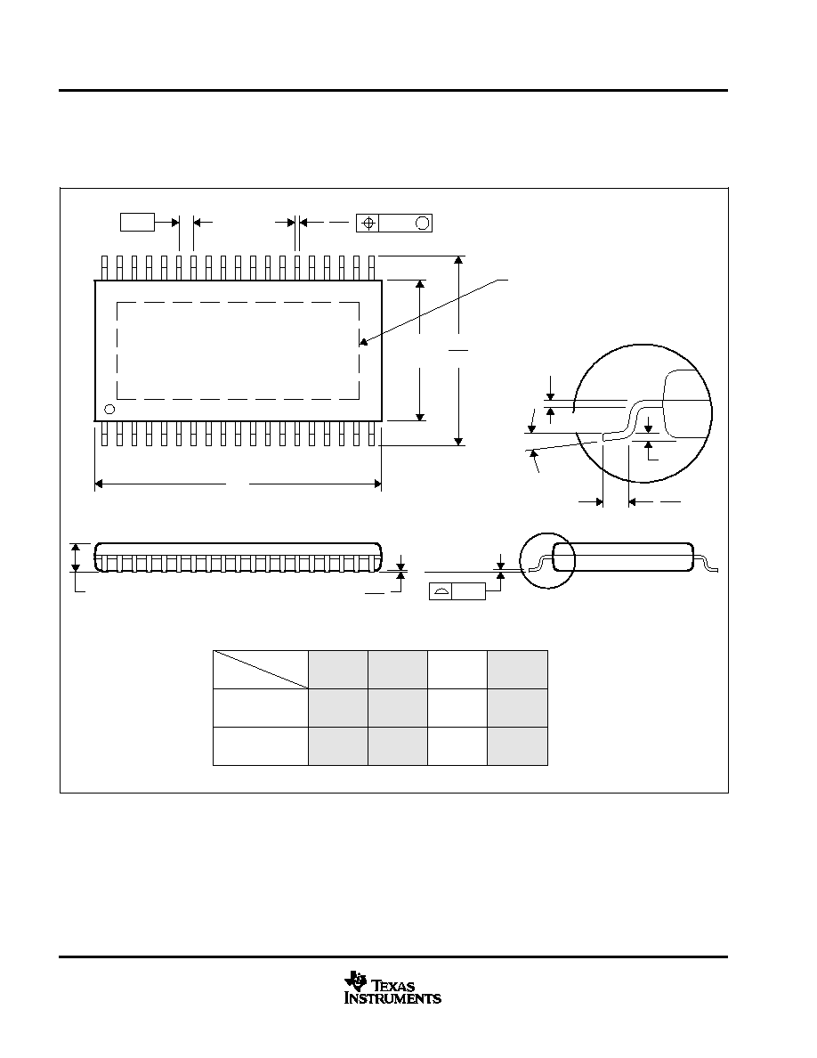
MECHANICAL DATA
DAP (R-PDSO-G**)
PowerPAD
PLASTIC SMALL-OUTLINE PACKAGE
0,25
0,75
0,50
0,15 NOM
Gage Plane
NOM
6,20
8,40
7,80
Thermal Pad
(see Note D)
38
12,60
11,10
32
Seating Plane
12,40
10,90
4073257/A 07/97
20
0,19
19
A
0,30
38
1
9,80
28
A MAX
PINS **
9,60
A MIN
DIM
1,20 MAX
10,90
11,10
30
38 PINS SHOWN
0,10
0,65
M
0,13
0
∞
≠ 8
∞
0,15
0,05
NOTES: A. All linear dimensions are in millimeters.
B. This drawing is subject to change without notice.
C. Body dimensions do not include mold flash or protrusion.
D. The package thermal performance may be enhanced by bonding the thermal pad to an external thermal plane. This pad is electrically
and thermally connected to the backside of the die and possibly selected leads. Thermal pad size is 3,86 mm X 3,91 mm for the
32-pin TAS5110 device.
E. Falls within JEDEC MO-153
PowerPAD is a trademark of Texas Instruments.

TAS5110
SLES028A ≠ MAY 2002 ≠ REVISED SEPTEMBER 2002
19
www.ti.com
MECHANICAL DATA
DAD (R-PDSO-G**)
PowerPAD
PLASTIC SMALL-OUTLINE (DIE DOWN)
0,25
0,75
0,50
0,15 NOM
Gage Plane
NOM
6,20
8,40
7,80
(See Note D)
Thermal Pad
38
12,60
32
11,10
Seating Plane
12,40
10,90
4073258/A 01/98
20
0,19
19
A
0,30
38 PINS SHOWN
38
1
A MAX
PINS **
A MIN
DIM
1,20 MAX
10,90
11,10
30
0,10
0,65
M
0,13
0
∞
≠ 8
∞
0,15
0,05
NOTES: A. All linear dimensions are in millimeters.
B. This drawing is subject to change without notice.
C. Body dimensions include mold flash or protrusion.
D. The package thermal performance may be enhanced by attaching an external heatsink to the thermal pad.
This pad is electrically and thermally connected to the backside of the die and possibly selected leads.
E. Falls within JEDEC MO-153
PowerPAD is a trademark of Texas Instruments Incorporated.

IMPORTANT NOTICE
Texas Instruments Incorporated and its subsidiaries (TI) reserve the right to make corrections, modifications,
enhancements, improvements, and other changes to its products and services at any time and to discontinue
any product or service without notice. Customers should obtain the latest relevant information before placing
orders and should verify that such information is current and complete. All products are sold subject to TI's terms
and conditions of sale supplied at the time of order acknowledgment.
TI warrants performance of its hardware products to the specifications applicable at the time of sale in
accordance with TI's standard warranty. Testing and other quality control techniques are used to the extent TI
deems necessary to support this warranty. Except where mandated by government requirements, testing of all
parameters of each product is not necessarily performed.
TI assumes no liability for applications assistance or customer product design. Customers are responsible for
their products and applications using TI components. To minimize the risks associated with customer products
and applications, customers should provide adequate design and operating safeguards.
TI does not warrant or represent that any license, either express or implied, is granted under any TI patent right,
copyright, mask work right, or other TI intellectual property right relating to any combination, machine, or process
in which TI products or services are used. Information published by TI regarding third≠party products or services
does not constitute a license from TI to use such products or services or a warranty or endorsement thereof.
Use of such information may require a license from a third party under the patents or other intellectual property
of the third party, or a license from TI under the patents or other intellectual property of TI.
Reproduction of information in TI data books or data sheets is permissible only if reproduction is without
alteration and is accompanied by all associated warranties, conditions, limitations, and notices. Reproduction
of this information with alteration is an unfair and deceptive business practice. TI is not responsible or liable for
such altered documentation.
Resale of TI products or services with statements different from or beyond the parameters stated by TI for that
product or service voids all express and any implied warranties for the associated TI product or service and
is an unfair and deceptive business practice. TI is not responsible or liable for any such statements.
Mailing Address:
Texas Instruments
Post Office Box 655303
Dallas, Texas 75265
Copyright
2002, Texas Instruments Incorporated