
TAS5121
SLES086A - NOVEMBER 2003 - REVISED MARCH 2004
DIGITAL AMPLIFIER POWER STAGE
TM
FEATURES
D
100-W RMS Power (BTL) Into 4
With Less
Than 10% THD+N
D
80-W RMS Power (BTL) Into 4
With Less
Than 0.2% THD+N
D
0.05% THD+N at 1 W Into 4
D
Power Stage Efficiency Greater Than 90%
Into 4
Load
D
Self-Protecting Design
D
36-Pin
PSOP3 Package
D
3.3-V Digital Interface
D
EMI Compliant When Used With
Recommended System Design
APPLICATIONS
D
DVD Receiver
D
Home Theatre
D
Mini/Micro Component Systems
D
Internet Music Appliance
DESCRIPTION
The TAS5121 is a high-performance digital amplifier
power stage designed to drive a 4-
speaker up to 100 W.
The device incorporates PurePath Digital
technology
and can be used with a TI audio PWM processor and a
simple passive demodulation filter to deliver high-quality,
high-efficiency digital audio amplification.
The efficiency of this digital amplifier can be greater than
90%, depending on the system design. Overcurrent
protection, overtemperature protection, and undervoltage
protection are built into the TAS5121, safeguarding the
device and speakers against fault conditions that could
damage the system.
P - Power - W
RL = 4
TC = 75
�
C
Gain = 3 dB
THD+N - T
otal Harmonic Distortion + Noise - %
TOTAL HARMONIC DISTORTION + NOISE
vs
POWER
0.1
1
10
100
10
1
0.01
0.1
PVDD_X - H-Bridge Voltage - V
0
10
20
30
40
50
60
70
80
90
0
4
8
12
16
20
24
28
32
P
O
- Output Power - W
UNCLIPPED OUTPUT POWER
vs
H-BRIDGE VOLTAGE
8
4
6
PurePath Digital and PowerPAD are trademarks of Texas Instruments.
Other trademarks are the property of their respective owners.
PRODUCTION DATA information is current as of publication date. Products
conform to specifications per the terms of Texas Instruments standard warranty.
Production processing does not necessarily include testing of all parameters.
Please be aware that an important notice concerning availability, standard warranty, and use in critical applications of Texas Instruments
semiconductor products and disclaimers thereto appears at the end of this data sheet.
www.ti.com
Copyright
2004, Texas Instruments Incorporated

TAS5121
SLES086A - NOVEMBER 2003 - REVISED MARCH 2004
www.ti.com
2
These devices have limited built-in ESD protection. The leads should be shorted together or the device placed in conductive foam during
storage or handling to prevent electrostatic damage to the MOS gates.
GENERAL INFORMATION
Terminal Assignment
The TAS5121 is offered in a thermally enhanced 36-pin
PSOP3 (DKD) package. The DKD package has the
thermal pad on top.
1
2
3
4
5
6
7
8
9
10
11
12
13
14
15
16
17
18
36
35
34
33
32
31
30
29
28
27
26
25
24
23
22
21
20
19
GND
PWM_BP
GND
RESET
DREG_RTN
GVDD
M3
DREG
DGND
M1
M2
DVDD
SD
DGND
OTW
GND
PWM_AP
GND
GVDD_B
GVDD_B
GND
BST_B
PVDD_B
PVDD_B
OUT_B
OUT_B
GND
GND
OUT_A
OUT_A
PVDD_A
PVDD_A
BST_A
GND
GVDD_A
GVDD_A
DKD PACKAGE
(TOP VIEW)
ABSOLUTE MAXIMUM RATINGS
over operating free-air temperature range unless otherwise noted(1)
TAS5121
UNITS
DVDD TO DGND
�0.3 V to 4.2 V
GVDD_x TO GND
14.2 V
PVDD_X TO GND (dc voltage)
33.5 V
PVDD_X TO GND(2))
48 V
OUT_X TO GND (dc voltage)
33.5 V
OUT_X TO GND(2))
48 V
BST_X TO GND (DC voltage)
46 V
BST_X TO GND(2))
53 V
PWM_XP, RESET, M1, M2, M3, SD,
OTW
�0.3 V to DVDD + 0.3 V
Maximum junction temperature range,
TJ
�40
�
C to 150
�
C
Storage temperature
�40
�
C to 125
�
C
(1) Stresses beyond those listed under "absolute maximum ratings"
may cause permanent damage to the device. These are stress
ratings only, and functional operation of the device at these or any
other conditions beyond those indicated under "recommended
operating conditions" is not implied. Exposure to absolute-
maximum-rated conditions for extended periods may affect device
reliability.
(2) The duration should be less than 100 ns (see application note
SLEA025).
ORDERING INFORMATION
TA
PACKAGE
TRANSPORT
MEDIA
DESCRIPTION
0
�
C to 70
�
C
TAS5121DKD
Tube
36-pin PSOP3
0
�
C to 70
�
C
TAS5121DKDR
Tape and reel
36-pin PSOP3
PACKAGE DISSIPATION RATINGS
PACKAGE
R
JC
(
�
C/W)
R
JA
(
�
C/W)
36-Pin DKD PSOP3
0.85
See Note 1
(1) The TAS5121 package is thermally enhanced for conductive
cooling using an exposed metal pad area. It is impractical to use the
devices with the pad exposed to ambient air as the only heat sinking
of the device.
For this reason, R
JA, a system parameter that characterizes the
thermal treatment, is provided in the Application Information section
of the data sheet. An example and discussion of typical system
R
JA values are provided in the Thermal Information section. This
example provides additional information regarding the power
dissipation ratings. This example should be used as a reference to
calculate the heat dissipation ratings for a specific application.

TAS5121
SLES086A - NOVEMBER 2003 - REVISED MARCH 2004
www.ti.com
3
Terminal Functions
TERMINAL
FUNCTION(1)
DESCRIPTION
NAME
DKD
FUNCTION(1)
DESCRIPTION
BST_A
22
P
High-side bootstrap supply (BST), external resistor and capacitor to OUT_A required
BST_B
33
P
High-side bootstrap supply (BST), external resistor and capacitor to OUT_B required
DGND
9, 14
P
I/O reference ground
DREG
8
P
Digital supply voltage regulator decoupling pin, 1-
�
F capacitor connected to DREG_RTN
DREG_RTN
5
P
Decoupling return pin
DVDD
12
P
I/O reference supply input: 100
to DREG, decoupled to GND, 0.1-
�
F capacitor connected to
GND
GND
1, 3, 16,
18, 21,
27, 28,
34
P
Power ground, connected to system GND
GVDD
6
P
Local GVDD decoupling \pin
GVDD_A
19, 20
P
Gate drive input voltage
GVDD_B
35, 36
P
Gate drive input voltage
M1
10
I
Protection mode selection pin, connect to GND
M2
11
I
Protection mode selection pin, connect to DREG
M3
7
I
Output mode selection pin; connect to GND
OTW
15
O
Overtemperature warning output, open drain with internal pullup resistor, active-low when temper-
ature exceeds 115
�
C
OUT_A
25, 26
O
Output, half-bridge A
OUT_B
29, 30
O
Output, half-bridge B
PVDD_A
23, 24
P
Power supply input for half-bridge A
PVDD_B
31, 32
P
Power supply input for half-bridge B
PWM_AP
17
I
PWM input signal, half-bridge A
PWM_BP
2
I
PWM input signal, half-bridge B
RESET
4
I
Reset signal, active-low
SD
13
O
Shutdown signal for half-bridges A and B (open drain with internal pullup resistor), active-low
(1) I = input, O = Output, P = Power
TAS5121
SLES086A - NOVEMBER 2003 - REVISED MARCH 2004
www.ti.com
4
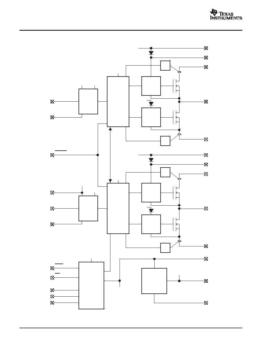
FUNCTIONAL BLOCK DIAGRAM
Protection
Logic
OT
and
UVP
GVDD
DREG
DREG_RTN
PWM
Receiver
Timing
Control
and
Protection
Gate
Drive
Gate
Drive
PWM_AP
OUT_A
GND
PVDD_A
BST_A
DREG
GVDD_A
OCH
OCL
Timing
Control
and
Protection
Gate
Drive
Gate
Drive
PWM_BP
OUT_B
GND
PVDD_B
BST_B
GVDD_B
OCH
OCL
M1
M2
DGND
DGND
DVDD
M3
OTW
SD
RESET
GVDD_A
DVDD DREG
DREG
GVDD_A
DVDD
DREG
DREG
DREG
DREG
GVDD_B
GVDD_B
PWM
Receiver
Internally
Connected
to GVDD_x

TAS5121
SLES086A - NOVEMBER 2003 - REVISED MARCH 2004
www.ti.com
5
RECOMMENDED OPERATING CONDITIONS
MIN
TYP
MAX
UNIT
DVDD
Digital supply (1)
Relative to DGND
3
3.3
3.6
V
GVDD_x
Supply for internal gate drive and logic
regulators
Relative to GND
10.8
12
13.2
V
PVDD_x
Half-bridge supply
Relative to GND, RL= 4
0
30.5
32
V
TJ
Junction temperature
0
125
_
C
(1) It is recommended for DVDD to be connected to DREG via a 100-
resistor.
ELECTRICAL CHARACTERISTICS
PVDD_X = 30.5 V, GVDD_x = 12 V, DVDD connected to DREG via a 100-
resistor, RL = 4
, 8X fs = 384 kHz, TAS5026 PWM processor,
unless otherwise noted
TYPICAL
OVER TEMPERATURE
SYMBOL
PARAMETER
TEST CONDITIONS
TA=25
�
C
TA=25
�
C
TC=75
�
C
UNITS
MIN/TYP/
MAX
AC PERFORMANCE, BTL Mode, 1 kHz
RL = 4
, THD = 10%, AES17
filter
100
W
Typ
Po
Output power
RL = 4
, THD = unclipped,
AES17 filter
80
W
Typ
RL = 8
, THD =unclipped,
AD mode
44
W
Typ
Po = 1 W/ channel, RL = 4
,
AES17 filter
0.05
%
Typ
THD+N
Total harmonic distortion + noise
Po = 10 W/channel, RL = 4
,
AES17 filter
0.1
%
Typ
Po = 80 W/channel, RL = 4
,
AES17 filter
0.2
%
Typ
Vn
Output integrated noise voltage
A-weighted, RL = 4
,
20 Hz to 20 kHz, AES17 filter
300
�
V
Max
SNR
Signal-to-noise ratio
A-weighted, AES17 filter
95
dB
Typ
DR
Dynamic range
f = 1 kHz, -60 dB,
A-weighted, AES17 filter
95
dB
Typ

TAS5121
SLES086A - NOVEMBER 2003 - REVISED MARCH 2004
www.ti.com
6
ELECTRICAL CHARACTERISTICS
PVDD_X = 30.5 V, GVDD_x = 12 V, DVDD connected to DREG via a 100-
resistor, RL = 4
, 8X fs = 384 kHz, TAS5026 PWM processor,
unless otherwise noted
TYPICAL
OVER TEMPERATURE
SYMBOL
PARAMETER
TEST CONDITIONS
TA=25
�
C
TA=25
�
C
TC=75
�
C
UNITS
MIN/TYP/
MAX
INTERNAL VOLTAGE REGULATOR AND CURRENT CONSUMPTION
DREG
Voltage regulator
Io = 1 mA
3.3
V
Min
DREG
Voltage regulator
Io = 1 mA
3.3
V
Max
IGVDD_x
Total GVDD supply current, operating
fS = 384 kHz, no load,
50% duty cycle
24
30
mA
Max
IDVDD
DVDD supply current, operating
fS = 384 kHz, no load
1
5
mA
Max
OUTPUT STAGE MOSFETs
RDSon,LS Forward on-resistance, low side
TJ = 25
�
C
120
132
m
Max
RDSon,HS Forward on-resistance, high side
TJ = 25
�
C
120
132
m
Max
INPUT/OUTPUT PROTECTION
Vuvp,G
Undervoltage protection limit, GVDD
7.6
7
V
Min
Vuvp,G
Undervoltage protection limit, GVDD
7.6
8.2
V
Max
OTW
Overtemperature warning
Static
115
�
C
Typ
OTE
Overtemperature error
Static
150
�
C
Typ
OC
Overcurrent protection
See Note 1.
9.5
A
Min
STATIC DIGITAL INPUT SPECIFICATION, PWM, PROTECTION MODE SELECTION PINS AND OUTPUT MODE SELECTION PINS
VIH
High-level input voltage
2
V
Min
VIH
High-level input voltage
DVDD
V
Max
VIL
Low-level input voltage
0.8
V
Max
Leakage
Input leakage current
-10
�
A
Min
Leakage
Input leakage current
10
�
A
Max
OTW/SHUTDOWN (SD)
Internal pullup resistor from OTW and
SD to DVDD
32
22
k
Min
VOL
Low-level output voltage
IO = 1 mA
0.4
V
Max
(1) To optimize device performance and prevent overcurrent (OC) protection activation, the demodulation filter must be designed with special care.
See Demodulation Filter Design in the Application Information section of the data sheet and consider the recommended inductors and capacitors
for optimal performance. It is also important to consider PCB design and layout for optimum performance of the TAS5121.

TAS5121
SLES086A - NOVEMBER 2003 - REVISED MARCH 2004
www.ti.com
7
TYPICAL APPLICATION AND CHARACTERIZATION CONFIGURATION USED WITH TAS5026
PWM PROCESSOR
TAS5121DKD
21
20
5
14
12
11
10
9
8
GVDD_B
OUT_A
GND
PVDD_A
GND
PVDD_B
PVDD_B
PVDD_A
OUT_B
31
32
34
BST_B
OUT_B
33
GND
OUT_A
35
30
28
26
29
27
BST_A
GND
GVDD_A
23
25
22
24
7
15
16
17
13
6
2
3
4
10
�
H
10
�
H
4.7 k
1000
�
F
PWM_AP_1
PWM_BP_1
1
�
F
100
nF
100
2.7
2.7
100 nF
33 nF
100 nF
33 nF
1
�
F
100 nF
H-Bridge
Power Supply
Gate-Drive
Power Supply
4.7 k
75 nH LPCB
PWM_AP
GVDD
GND
M2
M1
DREG
M3
DGND
RESET
OTW
DGND
SD
DVDD
DREG_RTN
GND
PWM_BP
1
1
1
GND
GVDD_B
36
18
GND
19
GVDD_A
Voltage suppressor diodes: 1SMA33CAT3
LPCB : Track in the PCB 1,0 mm wide and 50 mm long)
22
33
�
F
1
�
F
TVS Zener
TVS Zener
22
1
�
F
75 nH LPCB
1
�
F
Micro-
controller

TAS5121
SLES086A - NOVEMBER 2003 - REVISED MARCH 2004
www.ti.com
8
Figure 1
P - Power - W
RL = 4
TC = 75
�
C
Gain = 3 dB
THD+N - T
otal Harmonic Distortion + Noise - %
TOTAL HARMONIC DISTORTION + NOISE
vs
POWER
0.1
1
10
100
10
1
0.01
0.1
Figure 2
PVDD_X - H-Bridge Voltage - V
0
10
20
30
40
50
60
70
80
90
0
4
8
12
16
20
24
28
32
P
O
- Output Power - W
UNCLIPPED OUTPUT POWER
vs
H-BRIDGE VOLTAGE
8
4
6
Figure 3
PO(Total) - Total Output Power - W
0
2
4
6
8
10
12
14
0
10
20
30
40
50
60
70
80
Power Loss - W
POWER LOSS
vs
TOTAL OUTPUT POWER
Figure 4
TC - Case Temperature -
�
C
0
10
20
30
40
50
60
70
80
90
100
-30
0
30
60
90
120
P
O
- Output Power - W
UNCLIPPED OUTPUT POWER
vs
CASE TEMPERATURE

TAS5121
SLES086A - NOVEMBER 2003 - REVISED MARCH 2004
www.ti.com
9
Figure 5
PO(Total) - Total Output Power - W
0
10
20
30
40
50
60
70
80
90
100
0
10
20
30
40
50
60
70
80
- Efficiency - %
EFFICIENCY
vs
TOTAL OUTPUT POWER
Figure 6
f - Frequency - Hz
RL = 4
TC = 75
�
C
THD+N - T
otal Harmonic Distortion + Noise - %
TOTAL HARMONIC DISTORTION + NOISE
vs
FREQUENCY
20
100
1k
20k
1
0.1
0.001
0.01
10k
10 W
75 W
1 W
Figure 7
-0.5
-0.4
-0.3
-0.2
-0.1
-0.0
0.1
0.2
0.3
0.4
0.5
f - Frequency - Hz
PO = 1 W
TC = 75
�
C
AMPLITUDE
vs
FREQUENCY
10
100
1k
20k
10k
6
8
4
0.0
Amplitude - dBr A
Figure 8
f - Frequency - kHz
-160
-140
-120
-100
-80
-60
-40
-20
0
0
2
4
6
8
10
12
14
16
18
20
22
Amplitude - dBr A
AMPLITUDE
vs
FREQUENCY

TAS5121
SLES086A - NOVEMBER 2003 - REVISED MARCH 2004
www.ti.com
10
THEORY OF OPERATION
POWER SUPPLIES
This power device requires only two power supply
voltages, GVDD_x and PVDD_x.
GVDD_x is the gate drive supply for the device, which is
usually supplied from an external 12-V power supply.
GVDD_x is also connected to an internal LDR that
regulates the GVDD_x voltage down to the logic power
supply, 3.3 V, for the TAS5121 internal logic blocks. Each
GVDD_x pin is decoupled to system ground by a 1-
�
F
capacitor.
PVDD_x is the H-bridge power supply. Two power pins are
provided for each half-bridge due to the high current
density. It is important to follow the circuit and PCB layout
recommendations for the design of the PVDD_x
connection. For component suggestions, see the Typical
System Configuration section in this document. For layout
guidelines, see the reference design layout for the
TAS5121. Following these recommendations is important
because they influence key system parameters such as
EMI, idle current, and audio performance.
When GVDD_x is applied, while RESET is held low, the
error latches are cleared, SHUTDOWN is set high, and the
outputs are held in a high-impedance state. The bootstrap
capacitor is charged by the current path through the
internal bootstrap diode and external resistors placed on
the PCB from each OUT_x pin to ground. A subsequent
section describes the charging of the bootstrap capacitor.
Ideally, PVDD_x is applied after GVDD_x. When GVDD_x
and PVDD_x are applied, the TAS5121 is ready for
operation. PWM input signals can then be applied any time
during the power-on sequence, but they must be active
and stable before RESET is set high.
RECOMMENDATIONS FOR POWERING UP
RESET
GVDD
PVDD_X
PWM_xP
> 1 ms
> 1 ms
The following table describes the input conditions and the
output states of the device:
INPUTS
OUTPUTS
Condition
RESET
PWM
_AP
PWM
_BP
SHUT-
DOWN
OUT_
A
OUT_
B
Condition
Description
X
X
X
0
Hi-Z
Hi-Z
Shutdown
0
X
X
1
Hi-Z
Hi-Z
Reset
1
0
0
1
GND
GND
1
0
0
1
PVDD
PVDD
Normal
1
0
1
1
GND
PVDD
Normal
1
1
1
1
PVDD
PVDD
Reserved
After the previously mentioned conditions are met, the
device output begins. If PWM_AP is equal to a high and
PMW_BP is equal to a low, the high-side MOSFET in the
A half-bridge of the output H-bridge conducts while the
low-side MOSFET in the A half-bridge is not conducting.
Because the source of the high-side MOSFET is
referenced to the drain of the low-side MOSFET, a
bootstrapped gate drive is used to eliminate the need for
additional high-voltage power supplies. Under the above
condition, the opposite is true for the B half-bridge of the
output H-bridge. The low-side MOSFET in B half-bridge
conducts while the high-side MOSFET is not conducting;
therefore, the load connected between the OUT_A and
OUT_B pins has PVDD applied to it from the A side while
ground is applied from the B side for the period of time
PWM_AP is high and PWM_BP is low. Furthermore, when
the PWM signals change to the condition where PWM_AP
is low and PWM_BP is high, the opposite condition exists.
A constant high level is not permitted on the PWM inputs.
This condition causes the bootstrap capacitors to
discharge and can cause device damage.

TAS5121
SLES086A - NOVEMBER 2003 - REVISED MARCH 2004
www.ti.com
11
A digitally controlled dead-time circuit controls the
transitions between the high-side and low-side MOSFETs
to ensure that both devices in each half-bridge are not
conducting simultaneously.
POWERING DOWN
For power down of the TAS5121, an opposite approach is
necessary. The RESET must be asserted LOW before the
valid PWM signal is removed.
PRECAUTION
The TAS5121 must always start up in the high-impedance
(Hi-Z) state. In this state, the bootstrap (BST) capacitor is
precharged by a resistor on each PWM output node to
ground. See the system configuration. This ensures that
the TAS5121 is ready for receiving PWM pulses, indicating
either HIGH- or LOW-side turnon after RESET is
de-asserted to the back end.
With the following pulldown resistor and BST capacitor
size, the BST charge time is:
C = 33 nF, R = 4.7
k
R
�
C
�
5 = 775.5
�
s
After GVDD has been applied, it takes approximately 800
�
s to fully charge the BST capacitor. During this time,
RESET must be kept low. After approximately 1 ms the
back end BST is charged and ready. RESET can now be
released if the PWM modulator is ready and is streaming
valid PWM signals to the device. Valid PWM signals are
switching PWM signals with a frequency between
350-400 kHz. A constant HIGH level on the PWM+ forces
the high-side MOSFET ON until it eventually runs out of
BST capacitor energy. Putting the device in this condition
should be avoided.
In practice this means that the DVDD-to-PWM processor
(front-end) should be stable and initialization should be
completed before RESET is de-asserted to the TAS5121.
CONTROL I/O
Shutdown Pin: SD
The SD pin functions as an output pin and is intended for
protection-mode signaling to, for example, a controller or
other front-end device. The pin is open-drain with an
internal pullup resistor to DVDD.
The logic output is, as shown in the following table, a
combination of the device state and RESET input:
SD
RESET
DESCRIPTION
0
0
Reserved
0
1
Device in protection mode, i.e., UVP and/or OC
and/or OT error
1(2)
0
Device set high-impedance (Hi-Z), SD forced high
1
1
Normal operation
(2) SD is pulled high when RESET is asserted low independent of chip
state (i.e., protection mode). This is desirable to maintain
compatibility with some TI PWM front ends.
Overtemperature Warning Pin: OTW
The OTW pin gives a temperature warning signal when
temperature exceeds the set limit. The pin is of the
open-drain type with an internal pullup resistor to DVDD.
OTW
DESCRIPTION
0
Junction temperature higher than 115
�
C
1
Junction temperature lower than 115
�
C
Overall Reporting
The SD pin, together with the OTW pin, gives chip state
information as described in Table 1.
Table 1. Error Signal Decoding
OTW
SD
DESCRIPTION
0
0
Overtemperature error (OTE)
0
1
Overtemperature warning (OTW)
1
0
Overcurrent (OC) or undervoltage (UVP) error
1
1
Normal operation, no errors/warnings
Chip Protection
The TAS5121 protection function is generally
implemented in a closed loop control system with, for
example, a system controller. The TAS5121 contains three
individual systems protecting the device against fault
conditions. All of the error events result in the output stage
being set in a high-impedance state (Hi-Z) for maximum
protection of the device and connected equipment.
The device can be recovered by toggling RESET low and
then high, after all errors are cleared. It is recommended
that if the error persists, the device is held in reset until user
intervention clears the error.
Overcurrent (OC) Protection
The device has individual current protection on both
high-side and low-side power stage FETs. The OC
protection works only with the demodulation filter present
at the output. See Filter Demodulation Design in the
Application Information section of the data sheet for design
constraints.

TAS5121
SLES086A - NOVEMBER 2003 - REVISED MARCH 2004
www.ti.com
12
Overtemperature (OT) Protection
A dual temperature protection system asserts a warning
signal when the device junction temperature exceeds
115
�
C and shuts down the device when the junction
temperature exceeds 150
�
C. The OT protection circuit is
shared by both half-bridges.
Undervoltage Protection (UVP)
Undervoltage lockout occurs when GVDD is insufficient
for proper device operation. The UV protection system
protects the device under fault power-up and power-down
situations by shutting the device down. The UV protection
circuits are shared by both half-bridges.
Reset Function
The reset has two functions:
D
Reset is used for re-enabling operation after a
latched error event.
D
Reset is used for disabling output stage
switching, hard mute function. Use modulator
control for soft mute.
In protection modes where the reset input functions as the
means to re-enable operation after an error event, the error
latch is cleared on the falling edge of reset and normal
operation is resumed on the rising edge of RESET.
PROTECTION MODE
Autorecovery (AR) After Errors (PMODE0)
In autorecovery mode (PMODE0) the TAS5121 is
self-supported in handling of error situations. All protection
systems are active, setting the output stage in the
high-impedance state to protect the output stage and
connected equipment. However, after a short time the
device autorecovers, i.e., operation is automatically
resumed provided that the system is fully operational.
The autorecovery timing is set by counting PWM input
cycles, i.e., the timing is relative to the switching frequency.
The AR system is common to both half-bridges.
Timing and Function
The function of the autorecovery circuit is as follows:
1.
An error event occurs and sets the
protection latch (output stage goes Hi-Z).
2.
The counter is started.
3.
After n/2 cycles, the protection latch is
cleared but the output stage remains Hi-Z
(identical to pulling RESET low).
4.
After n cycles, operation is resumed
(identical to pulling RESET high) (n = 512).
Error
Protection
Latch
Shutdown
Autorecovery
SD
PWM
Counter
AR-RESET
Figure 9. Autorecovery Function
Latching Shutdown on All Errors (PMODE1)
In latching shutdown mode, all error situations result in a
power down (output stage Hi-Z). Re-enabling can be done
by toggling the RESET pin.
All Protection Systems Disabled (PMODE2)
In PMODE2, all protection systems are disabled. This
mode is purely intended for testing and characterization
purposes and thus not recommended for normal device
operation.
MODE Pins Selection
The protection mode is selected by connecting M1/M2 to
DREG or DGND according to Table 2.
Table 2. Protection Mode Selection
M1
M2
PROTECTION MODE
0
0
Autorecovery after errors (PMODE 0)
0
1
Latched shutdown on all errors
1
0
Reserved
1
1
Reserved
The output configuration mode is selected by connecting
the M3 pin to DREG or DGND according to Table 3.

TAS5121
SLES086A - NOVEMBER 2003 - REVISED MARCH 2004
www.ti.com
13
Table 3. Output Mode Selection
M3
OUTPUT MODE
0
Bridge-tied load output stage (BTL)
1
Reserved
APPLICATION INFORMATION
DEMODULATION FILTER DESIGN
The TAS5121 amplifier outputs are driven by high-current
DMOS transistors in an H-bridge configuration. These
transistors are either off or fully on.
The result is a square-wave output signal with a duty cycle
that is proportional to the amplitude of the audio signal. It
is recommended that a second-order LC filter be used to
recover the audio signal.
Output A
C1
TAS5121
L
Output B
L
C2
R(Load)
Figure 10. Demodulation Filter
The main purpose of the demodulation filter is to attenuate
the high-frequency components of the output signals that
are out of the audio band.
Design of the demodulation filter affects the audio
performance of the power amplifier significantly. As a
result, to ensure proper operation of the overcurrent (OC)
protection circuit and meet the device THD+N
specifications, the selection of the inductors used in the
output filter must be considered according to the following.
The rule is that the inductance should remain stable within
the range of peak current seen at maximum output power
and deliver approximately 5
�
H of inductance at 15 A.
If this rule is observed, the TAS5121 should not have
distortion issues due to the output inductors. This prevents
device damage due to overcurrent conditions because of
inductor saturation in the output filter.
Another parameter to be considered is the idle current loss
in the inductor. This can be measured or specified as
inductor dissipation (D). The target specification for
dissipation is less than 0.05. If this specification is not met,
idle current increases.
In general, 10-
�
H inductors suffice for most applications.
The frequency response of the amplifier is slightly altered
by the change in output load resistance; however, unless
tight control of frequency response is necessary (better
than 0.5 dB), it is not necessary to deviate from 10
�
H.
The graphs in Figure 11 display the inductance vs current
characteristics of two inductors that are suggested for use
with the TAS5121.
Figure 11. Inductance Saturation
I - Current - A
4
5
6
7
8
9
10
11
0
5
10
15
L - Inductance -
�
H
INDUCTANCE
vs
CURRENT
DBF1310A
DASL983XX-1023
The selection of the capacitors that are placed from the
output of each inductor to ground is simple. To complete
the output filter, use a 1-
�
F capacitor with a voltage rating
at least twice the voltage applied to the output stage
(PVDD_x).
This capacitor should be a good quality polyester
dielectric.
THERMAL INFORMATION
The following is provided as an example.
The thermally enhanced package provided with the
TAS5121 are designed to be interfaced directly to
heatsinks using a thermal interface compound (for
example, Wakefield Engineering type 126 thermal
grease.) The heatsink then absorbs heat from the ICs and
transfers it to the ambient air. If the heatsink is carefully
designed, this process can reach equilibrium and heat can
be continually removed from the ICs without device
overtemperature shutdown. Because of the efficiency of
the TAS5121, heatsinks are smaller than those required
for linear amplifiers of equivalent performance.

TAS5121
SLES086A - NOVEMBER 2003 - REVISED MARCH 2004
www.ti.com
14
R
JA
is a system thermal resistance from junction to
ambient air. As such, it is a system parameter with roughly
the following components:
D
R
JC
(the thermal resistance from junction to
case, or in this case the metal pad)
D
Heatsink compound thermal resistance
D
Heatsink thermal resistance
The thermal grease thermal resistance can be calculated
from the exposed pad area and the thermal grease
manufacturer's area thermal resistance (expressed in
�
C-in
2
/W). The area thermal resistance of the example
thermal grease with a 0.001-inch thick layer is about 0.054
�
C-in
2
/W. The approximate exposed pad area is as
follows:
36-pin PSOP3
0.116 in
2
Dividing the example thermal grease area resistance by
the area of the pad gives the actual resistance through the
thermal grease for the device:
36-pin PSOP3
0.47
�
C/W
The thermal resistance of thermally conductive pads is
generally higher than a thin thermal grease layer. Thermal
tape has an even higher thermal resistance and should not
be used with this package.
Heatsink thermal resistance is generally predicted by the
heatsink vendor, modeled using a continuous flow
dynamics (CFD) model, or measured.
Thus, for a single monaural IC, the system R
JA
= R
JC
+
thermal grease resistance + heatsink resistance.
The following table indicates modeled parameters for one
TAS5121 IC on a heatsink. The junction temperature is set
at 110
�
C while delivering 70 W RMS into 4-
loads with no
clipping. It is assumed that the thermal grease is about
0.001 inch thick (this is critical).
Table 4. Example of Thermal Simulation
36-Pin PSOP3
Ambient temperature
25
�
C
Power to load
70 W
Delta T inside package
5.5
�
C
Delta T through thermal grease
3.2
�
C
Required heatsink thermal resistance
11.0
�
C/W
Junction temperature
110
�
C
System R
JA
12.3
�
C/W
R
JA * power dissipation
85
�
C
R
JC
0.85
�
C/W
As an indication of the importance of keeping the thermal
grease layer thin, if the thermal grease layer increases to
0.002 inches thick, the required heatsink thermal
resistance increases to 5.2
�
C/W for the PSOP3 package.
REFERENCES
1.
Digital Audio Measurements application report--TI
(SLAA114)
2.
PowerPAD
Thermally Enhanced Package
technical brief--TI (SLMA002)
3.
System Design Considerations for True Digital
Audio Power Amplifiers application report--TI
(SLAA117)
4.
Voltage Spike Measurement Technique and
Specification application note--TI (SLEA025)

TAS5121
SLES086A - NOVEMBER 2003 - REVISED MARCH 2004
www.ti.com
15
MECHANICAL DATA


IMPORTANT NOTICE
Texas Instruments Incorporated and its subsidiaries (TI) reserve the right to make corrections, modifications,
enhancements, improvements, and other changes to its products and services at any time and to discontinue
any product or service without notice. Customers should obtain the latest relevant information before placing
orders and should verify that such information is current and complete. All products are sold subject to TI's terms
and conditions of sale supplied at the time of order acknowledgment.
TI warrants performance of its hardware products to the specifications applicable at the time of sale in
accordance with TI's standard warranty. Testing and other quality control techniques are used to the extent TI
deems necessary to support this warranty. Except where mandated by government requirements, testing of all
parameters of each product is not necessarily performed.
TI assumes no liability for applications assistance or customer product design. Customers are responsible for
their products and applications using TI components. To minimize the risks associated with customer products
and applications, customers should provide adequate design and operating safeguards.
TI does not warrant or represent that any license, either express or implied, is granted under any TI patent right,
copyright, mask work right, or other TI intellectual property right relating to any combination, machine, or process
in which TI products or services are used. Information published by TI regarding third-party products or services
does not constitute a license from TI to use such products or services or a warranty or endorsement thereof.
Use of such information may require a license from a third party under the patents or other intellectual property
of the third party, or a license from TI under the patents or other intellectual property of TI.
Reproduction of information in TI data books or data sheets is permissible only if reproduction is without
alteration and is accompanied by all associated warranties, conditions, limitations, and notices. Reproduction
of this information with alteration is an unfair and deceptive business practice. TI is not responsible or liable for
such altered documentation.
Resale of TI products or services with statements different from or beyond the parameters stated by TI for that
product or service voids all express and any implied warranties for the associated TI product or service and
is an unfair and deceptive business practice. TI is not responsible or liable for any such statements.
Following are URLs where you can obtain information on other Texas Instruments products and application
solutions:
Products
Applications
Amplifiers
amplifier.ti.com
Audio
www.ti.com/audio
Data Converters
dataconverter.ti.com
Automotive
www.ti.com/automotive
DSP
dsp.ti.com
Broadband
www.ti.com/broadband
Interface
interface.ti.com
Digital Control
www.ti.com/digitalcontrol
Logic
logic.ti.com
Military
www.ti.com/military
Power Mgmt
power.ti.com
Optical Networking
www.ti.com/opticalnetwork
Microcontrollers
microcontroller.ti.com
Security
www.ti.com/security
Telephony
www.ti.com/telephony
Video & Imaging
www.ti.com/video
Wireless
www.ti.com/wireless
Mailing Address:
Texas Instruments
Post Office Box 655303 Dallas, Texas 75265
Copyright
2004, Texas Instruments Incorporated